
 Open Access Article
 This Open Access Article is licensed under a Creative Commons Attribution-Non Commercial 3.0 Unported Licence
Novel hybrid Si film/carbon nanofibers as anode materials in lithium-ion batteries†
Haejune
Kim‡
,
Xingkang
Huang‡
,
Zhenhai
Wen
,
Shumao
Cui
,
Xiaoru
Guo
and
Junhong
Chen
*
Department of Mechanical Engineering, University of Wisconsin-Milwaukee, 3200 N Cramer Street, Milwaukee, WI 53211, USA. E-mail: jhchen@uwm.edu; Fax: +1-414-229-6958; Tel: +1-414-229-2615
First published on 23rd December 2014
Abstract
The hybrid Si film/carbon nanofiber (CNF) as an anode in lithium-ion batteries (LIBs) was synthesized using a two-step chemical vapour deposition (CVD) method. This binder- and conductive additive-free electrode delivered a discharge capacity of 1000 mA h g−1 over 200 cycles. CNFs as a support material were directly grown on a stainless steel foil, while the stress-resilient Si films coated on the CNFs offered high Li storage capacity.
Lithium-ion batteries (LIBs) are the most widely used energy storage systems, powering portable electronic devices, power tools and current/future electric vehicles due to their high energy density.1 The performance of LIBs greatly depends on the properties of electrodes. Thus, the choice of electrode materials and their structural/morphological characteristics especially at the nanometer scale are the critical factors determining the performance of LIBs.2–4 Graphite is the most commonly used anode material in commercial LIBs, but the graphite-based electrode in today's battery technology has almost reached its theoretical capacity limit bound by 372 mA h g−1.5 Indeed, new electrode materials need to be developed to fulfill today's high energy demands.
Silicon has been considered as one of the most promising anode materials to replace graphite electrodes due to its high theoretical energy density (3590 mA h g−1 in Li15Si4 at room temperature). However, the large volume change of Si over 300% during the Li alloying/de-alloying results in the pulverization of Si, leading to the loss of electrical contacts between the current collector and the active materials, thus hindering the commercialization of Si-based electrodes.2,3,6 In addition, the huge volume change in Si leads to an unstable solid-electrolyte interface (SEI) formation by disintegrating the SEI layer and exposing new Si surfaces to the electrolyte continually after repeated charge/discharge cycles.7,8 As a result, a thick SEI layer is formed, which increases the electronic resistivity, and thus decreases the charge capacity due to the slow Li-ion transport.
The large stress in the Si materials is generally alleviated by reducing the size of the Si materials. Various types of Si nanostructures such as nanoparticles,2,9,10 nanotubes,11–14 nanowires,3,15,16 and nanofilms17,18 have been examined as anode electrodes in LIBs to optimize the battery performance toward high energy/power density and long cycle life by controlling the degree of volume change. The nanostructured Si/Si-based electrodes have shown superior performance compared with bulk Si electrodes. However, the challenges of scalability, high cost and a relatively short cycle life remain.
Excellent cycle performance of the Si-based electrode has been achieved when silicon is used in the form of a few tens of nanometer-thin film since the nano-scale film thickness efficiently mitigates the mechanical stress during Li alloying/dealloying. The Si film can be synthesized by a low pressure chemical vapor deposition (LPCVD) method,19,20 magnetron sputtering,18,21 and vacuum evaporation.22 LPCVD is the most favorable method for conformal deposition of Si on a complex-shaped substrate, which is important for the uniform distribution of the internal stress in Si materials during cycles. The thickness of the Si film is controllable by the SiH4 flow rate and the growth duration. Excellent cycle performance was demonstrated with 250 nm Si film, while the loading amount of Si thin films on the as-received current collectors was very limited.23 On the other hand, increasing the loading density by using a Si thick film such as 1 μm exhibits poor cycle stability. Several research groups have demonstrated that a chemically or mechanically roughened substrate improves the cycle stability by increasing the adhesion force between the Si film and the substrate.18,22 The roughened substrate generates interlocking shapes being filled with Si and hold the Si film more tightly to the substrate. To increase the loading density of the active materials, a new supporting structure is necessary to provide a large surface area to increase the loading density of Si films, good electrical conductivity to enhance electron transfer, and mechanical flexibility to relieve the stress. Wang et al. designed a vertically aligned carbon nanotube (VACNT) decorated with Si nanoparticles.24 In a similar fashion, Evanoff et al. synthesized a Si film/VACNT hybrid structure to circumvent the issue and showed excellent loading density and electrochemical performance.25
Here, we investigate new hybrid materials based on carbon nanofibers (CNFs) and Si films for stable and high energy-anode materials in LIBs. The novelty of our research is on a facile synthesis process to produce Si- and carbon-based hybrid electrodes by modifying the current collector to favor Si film deposition. The CNFs that serve as a supporting matrix for Si films provide a large surface area, good electrical conductivity, and economical synthesis processes. The electrolyte can easily penetrate a porous CNF network and increase the contact area between the electrolyte and the active materials. Individual CNFs make direct contact with the current collectors, providing a fast and efficient electron transfer pathway.
To synthesize CNFs directly on a stainless steel substrate, we modified a CNT growth method described by Baddour et al.,26 namely, using concentrated hydrochloric acid (HCl) to etch the surface oxide of the stainless steel and forming catalysts by thermal annealing for CNT growth.27 High iron and nickel contents in type 304 stainless steel (Fe![[thin space (1/6-em)]](https://www.rsc.org/images/entities/char_2009.gif) :Cr:Ni = 70:19:11 wt%, Alfa Aesar) facilitate the growth of CNFs.28,29 The growth process consists of three steps: acid treatment, heat treatment, and CVD growth. The 25 μm thick stainless steel foil was ultrasonicated in acetone for 30 min. The type 304 stainless steel foil contains a high iron and nickel content (81% in weight). However, the passive film of chromium (Cr2O3) on the surface prevents the carbon precursors in the CVD process from reacting with iron and nickel.30 To remove the Cr2O3 film, the substrate was etched with 35 wt% HCl for 10 min. The acid-treated substrate was punched to disks (0.5 inch in diameter) and transferred to the CVD reactor; thermal annealing was carried out in argon at 850 °C for 30 min. After adjusting the temperature to 700 °C, the CNFs were grown at atmospheric pressure with a gas mixture of acetylene (C2H2) containing water vapor and hydrogen (H2). The gas flow ratio of C2H2 and H2 was fixed at 1:10 during the synthesis. The outlet of the CVD reactor was connected to an oil bubbler to prevent the air from flowing back into the reactor. When necessary, a layer of carbon can be coated on the as-produced Si/CNF composites using CVD with the C2H2 flow (0.03 mL min−1), which helps to improve the conductivity of the Si/CNF electrode and achieve stable electrochemical performance.
:Cr:Ni = 70:19:11 wt%, Alfa Aesar) facilitate the growth of CNFs.28,29 The growth process consists of three steps: acid treatment, heat treatment, and CVD growth. The 25 μm thick stainless steel foil was ultrasonicated in acetone for 30 min. The type 304 stainless steel foil contains a high iron and nickel content (81% in weight). However, the passive film of chromium (Cr2O3) on the surface prevents the carbon precursors in the CVD process from reacting with iron and nickel.30 To remove the Cr2O3 film, the substrate was etched with 35 wt% HCl for 10 min. The acid-treated substrate was punched to disks (0.5 inch in diameter) and transferred to the CVD reactor; thermal annealing was carried out in argon at 850 °C for 30 min. After adjusting the temperature to 700 °C, the CNFs were grown at atmospheric pressure with a gas mixture of acetylene (C2H2) containing water vapor and hydrogen (H2). The gas flow ratio of C2H2 and H2 was fixed at 1:10 during the synthesis. The outlet of the CVD reactor was connected to an oil bubbler to prevent the air from flowing back into the reactor. When necessary, a layer of carbon can be coated on the as-produced Si/CNF composites using CVD with the C2H2 flow (0.03 mL min−1), which helps to improve the conductivity of the Si/CNF electrode and achieve stable electrochemical performance.
Subsequently, Si thin films were deposited on the CNFs using LPCVD. The CVD reactor was sealed and purged with argon three times before increasing the temperature of the reactor. The pressure of the reactor was maintained below 30 Torr for uniform deposition of Si films over the substrate by increasing the mean free path of Si atoms at low pressure. When the temperature of the reactor reached 500 °C, 0.75% silane (SiH4, Airgas) in argon (Ar, Airgas) was supplied for a specific time, depending on the desirable thickness of Si films. The weight of the active materials was acquired by measuring the weight change before and after the Si deposition with a Sartorius CPA225D (0.01 mg in resolution). The typical mass loading of Si on the Si/CNF anode is 0.24–0.31 mg cm−2. The as-prepared Si/CNF hybrid materials on stainless steel were used for anode electrodes without further treatment. The coin-type half cell (CR2032) was assembled in a glove box under an argon atmosphere with oxygen and moisture levels below 1 ppm. Lithium metal foil was used as the counter and the reference electrode, and a Celgard 2325 trilayer porous polymer membrane was used as the separator. The electrolyte was composed of a 1 M LiPF6 solution in a carbonate mixture (ethylene carbonate/ethyl methyl carbonate = 40:60 by volume). The electrochemical performance was evaluated at room temperature using a Land Battery Test System in a galvanostatic mode.
CNFs were directly grown on type 304 stainless steel foils without applying additional catalysts such as iron deposition onto a substrate. Scanning electron microscopy (SEM) and transmission electron microscopy (TEM) observations were used to investigate the structure of CNFs. Fig. 1a shows a SEM image of CNFs grown on the stainless steel foil, covering the entire surface of the half-inch substrate in diameter. The CNF network was randomly entangled with diameters in the range of 100 to 400 nm. The diameter of the CNF is directly related to the size of the catalyst particle,31,32 indicating a wide range of catalyst sizes on the stainless steel after the pre-treatment process. Catalyst particles, as observed in Fig. 1a inset and Fig. 1b, were formed when annealing the HCl-etched stainless steel.27 The TEM image in Fig. 1b clearly shows that CNF has the catalyst particle at the tip of the fiber. In Fig. 1c, the selected area electron diffraction (SAED) pattern on the CNFs shows two concentric diffraction rings that correspond to the (002) and (101) planes of graphite; however, no distinct diffraction spots indicate poor graphitization of CNFs.
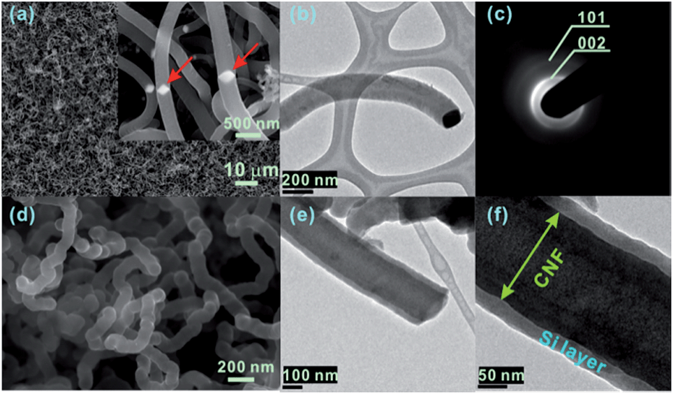 | ||
| Fig. 1 (a) SEM image of CNFs grown on type 304 stainless steel foil; red arrows point at catalyst particles in the inset. (b) TEM images of CNFs. CNFs were synthesized directly on type 304 stainless steel without adding any catalyst. (c) SAED pattern of CNFs. (d) SEM image of Si-deposited CNFs. (e and f) TEM images of Si-deposited CNF. TEM images show a cylindrical structure with a Si coating layer thickness of about 30 nm. | ||
The Si film was deposited on the CNF-grown stainless steel foil via LPCVD, as shown in Fig. 1d. The hybrid Si/CNF on stainless steel foil was ultrasonicated in ethanol to remove it from the substrate and transferred to the TEM grid. The TEM images of the Si/CNF in Fig. 1e and f show a distinct layer. The diameter of the CNFs is ∼150 nm and increases to ∼210 nm after Si film deposition, which indicates an Si film thickness of 30 nm after coating with Si films for 30 min. The presence of Si film can be observed through energy dispersive X-ray spectroscopy (EDS) studies. In Fig. S1(a)–(c),† EDS elemental analysis indicates that the Si films were uniformly coated on CNFs. The hybrid materials are composed of Si, C, O and the weak Cr and Fe peaks come from the underlying stainless steel substrate in Fig. S1(d).† The X-ray diffraction (XRD) result did not show any Si or silicide peaks (Fig. S2†), suggesting that the amount of Si is below the XRD detection threshold and no significant reactions occur between Si and the stainless steel substrate. A similar result was observed when Cu was used as a substrate as indicated in Fig. S3;† there was no obvious difference in the XRD pattern between Cu and Si-coated Cu. The only well-developed peaks were associated with the Cu substrate. Fig. S4† shows the Raman spectra of the Si/CNFs hybrid and CNFs. The Raman spectrum of the Si/CNF displays three well-defined peaks, a main peak at around 510 cm−1, slightly shifted away from the characteristic peak of a bulk Si (520 cm−1), which suggests that the Si film consists of nanocrystals. The other two peaks at 1360 cm−1 (defect-induced D band) and 1590 cm−1 (in-plane vibrational G band) are ascribed to graphitic carbon.
An electrochemical test was performed using the hybrid Si/CNF as a working electrode and lithium metal as a counter electrode. The specific capacity and Coulombic efficiency (CE) of the Si/CNF electrode vs. the cycle number are shown in Fig. 2a. In this study we defined the charge and discharge processes as lithiation and delithiation of Si, respectively. The Si/CNF exhibited high capacities with excellent cycle stability, which was possibly due to the stress-resistant nature of the Si thin film, the robust mechanical support, and the good electrical properties of CNFs. The nanometer-thin layer of the Si films allows fast diffusion of the Li ions to the core of the active materials. The weight ratio of the Si film to CNF was about 1:1. The contribution of the Li intercalation to the CNFs is less than 10% of the total capacity in the hybrid materials according to the theoretical capacity of Si and C, even when C is fully intercalated; thus, the specific capacity was calculated using the mass of Si.
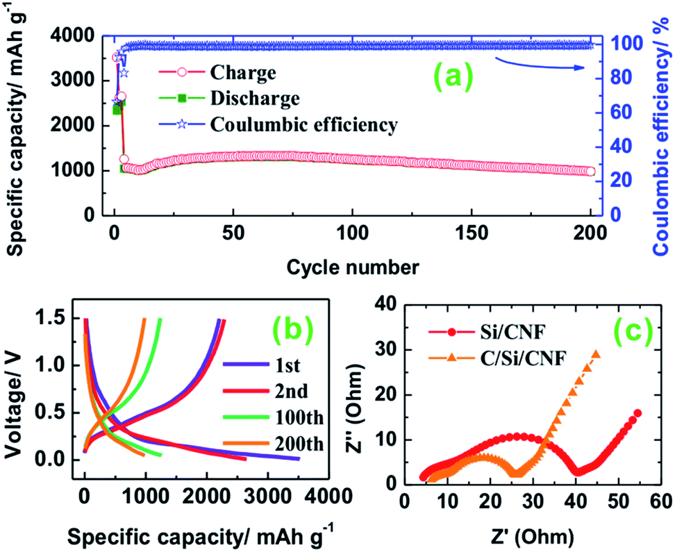 | ||
| Fig. 2 (a) Cycle performance (charge, discharge, and Coulombic efficiency or CE) of Si/CNF electrodes at a current rate of 0.05C (or 100 mA g−1) in the first 3 cycles, and at 1 C (or 2000 mA g−1) for the rest of the cycles. (b) Galvanostatic charge/discharge profiles of Si/CNF electrodes at a current rate of 0.05 C in the first 3 cycles, and 1 C for the rest of the cycles . (c) Nyquist plot of Si/CNF electrodes before and after carbon deposition. | ||
The cells were galvanostatically cycled at a low current rate of 0.05 C (1 C = 2000 mA g−1) between 0.01 and 2 V for the first three cycles to ensure a stable SEI film formation and a rearranged electrode structure due to the large volume changes during initial Li alloying/de-alloying. The current rate was increased to 1 C for the remaining cycles over the voltage window of 0.05–1.5 V to limit the state of lithiation. The reversible discharge capacity of the Si/CNF was about 1000 mA h g−1 over 200 cycles. There was a slight increase in the specific capacity from 10 to 80 cycles that resulted from increasing the Si atoms during activation. The major reason for the excellent cycle performance is ascribed to the structural integrity of the Si thin film without much degradation. The TEM observation of the Si/CNF anode suggests that the Si remained in close contact with the CNFs after 200 cycles (Fig. S5†); the thickness of the Si layer after cycling is approximately 36 nm, slightly larger than that before cycling. This result is further confirmed by SEM and EDS analyses of the Si/CNF anode after 200 cycles (Fig. 3). Compared with the pristine Si/CNF electrode (Fig. 1d), the electrode after cycling retained the fiber shape of the Si/CNFs, but with a rougher surface (Fig. 3a). For clearer observation, the Si/CNF anode was rinsed with acetone and then with a dilute HCl solution to remove the SEI layer on the Si surface and observed on a Cu grid (Fig. 3b–h). From the ends of the Si/CNFs, a layer of Si was well coated on the CNFs (Fig. 3c), which was further confirmed by the EDS analysis (Fig. 3e–h).
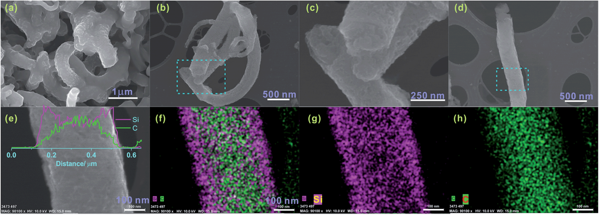 | ||
| Fig. 3 (a) SEM image of the top-view of the Si/CNF electrode, rinsed with dimethyl carbonate, and (b–h) SEM images and EDS analysis of the Si/CNFs observed on a Cu grid after washing with acetone and dilute HCl solution to remove the SEI layer; (c and e) are the closer observations of the rectangle-marked zones in (b and d), respectively. | ||
On the other hand, the capacity fade started slowly around 80 cycles, which may be attributed to the detachment of Si/CNFs from the stainless steel substrate, the delamination of the Si thin film from the CNF surface, and the disintegrated SEI film after the repeated volume change of the Si film. We noticed that some of the Si/CNFs detached from the stainless steel substrate when disassembling the coin cell after 200 cycles, which did not occur for the Si/CNF anode after 50 cycles. No obvious crack was observed on the Si surface; however, the surfaces of the Si/CNFs after cycling (Fig. 3a) look rougher than those before cycling (Fig. 1d). This suggests that the surface of the Si in the Si/CNF anode turned porous upon repeated cycling. The porosity formation of the Si/CNFs at the interface between the Si/CNFs and the stainless steel substrate may lead to a gradual loss of the electrical contact between Si/CNFs and the substrate, resulting in the capacity decay.
Fig. 2b shows typical galvanostatic charge/discharge profiles of the Si/CNF electrode at the current rate of 0.05 C in the first 3 cycles, and 1 C for the rest of the cycles. The specific charge/discharge capacities of the hybrid electrodes are 3522 mA h g−1 and 2341 mA h g−1, respectively, which indicates that the initial CE of the hybrid electrodes was ∼66%. There is an obvious difference between the first charge curve and the second one. The irreversible capacity in the first cycle is caused by the reductive decomposition of the electrolyte solution and the subsequent SEI film formation. After a few cycles, a high CE of >99% was achieved in the remaining cycles. In the first charge (Li alloying with Si) voltage profile, the voltage drops quickly to 0.3 V and gradually decreases to 0.01 V. The long plateau near 0 V is attributed to the lithium alloying with silicon and to form LixSi. The 100th and 200th charge/discharge profiles are very similar except for a slight capacity loss, suggesting that the hybrid materials retain their structure without distinctive degradation. In contrast, Simon et al.33 deposited uncoated CNFs onto continuous rolls of non-woven polyacrylonitrile derived carbon fibers (CFs) held together with a polymeric binder, which was followed by coating Si on the CNFs by a proprietary process. The as-synthesized Si/CNF electrode showed a capacity of ca. 985 mA h g−1, which decayed to 750 mA h g−1 in 20 cycles. Cui et al.34 prepared an Si-coated carbon nanowire anode by dropwise casting a commercial CNF onto a stainless steel substrate, followed by CVD growth of Si. The as-obtained Si/CNF anode delivered a capacity of ca. 2000 mA h g−1 at 2100 mA g−1, and retained 1600 mA h g−1 after 55 cycles.
As a comparison, the control electrodes were assembled and tested with CNFs alone. It was found that the specific capacity of CNFs only was approximately 200 mA h g−1 at a current rate of 300 mA g−1, much smaller than that of the hybrid electrodes as shown in Fig. S6.† Note that CNFs were reported with a high reversible capacity (e.g., ca. 500 mA h g−1) while delithiating to high voltage cutoffs (such as 3.0 V); below 1.5 V the capacity is approximately 250 mA h g−1,35 consistent with our CNF electrode. Cyclic voltammetry of the Si/CNF anode exhibited an anodic peak at ca. 1.7 V (Fig. S7†), which is associated with delithiation of LixC6. Despite the low capacity of the CNF electrode, it showed extremely stable cycle performance without distinctive degradation of capacity over 150 cycles. Considering the simple fabrication methods of CNFs, it is very promising to use a CNF electrode directly as an anode electrode without adding any conductive agents and polymeric binders. In Fig. S8† uniform CNFs were grown on both sides of 15 mm by 150 mm stainless steel foil whose size is only limited by the dimension of the tube furnace. Large-scale production of CNF electrodes is readily possible with an increased reactor size. However, the as-produced CNFs exhibit high irreversible capacity loss in the first cycle, which may be attributed to an irreversible Li-ion reaction with the oxygen-containing function group. Further research on reduction/electrochemical characteristics of CNF electrode is needed.
The rate performance of the hybrid Si/CNF was tested at various current rates as shown in Fig. 4. The reversible discharge capacity reached 2537, 2358, 2169, 1846, 1479, 1083, and 610 mA h g−1 at the current rates of 0.05, 0.1, 0.2, 0.5 C, 1 C, 2 C, and 5 C, respectively. The excellent rate capability is attributed to the short distance for Li-diffusion and electron transfer in the Si thin films.
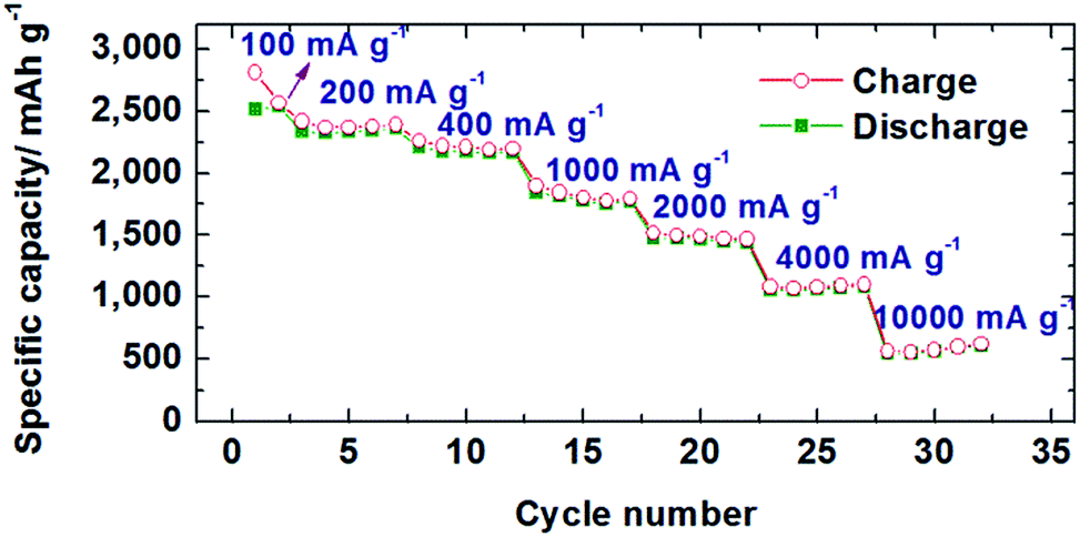 | ||
| Fig. 4 Rate capability of the hybrid Si/CNF at various current densities. | ||
Several studies reported that carbon coating on Si-based electrodes is an effective way to improve their electrochemical properties by suppressing the large consumption of electrolytes to form an SEI film and providing more conductive networks in the active materials while Li ion is permeable.10,36–38 The Nyquist plot was used to verify the improved electrical conductivity of the Si/CNF hybrid electrode by applying carbon coating on the surface of the Si film. As shown in Fig. 2c, electrochemical impedance spectroscopy (EIS) tests were conducted on both electrodes in the fully delithiated state after completing two charge/discharge cycles. The Si/CNF electrode with carbon coating exhibits a smaller semicircle at the medium-frequency zone, suggesting a smaller charge transfer resistance on the electrode/electrolyte compared with that of the Si/CNF electrode. Thus, coating an additional layer of C on the surface of the Si/CNF electrode may help to further improve the electrochemical performance, which is under investigation.
In summary, the novel Si/CNF hybrid materials were obtained by a two-step CVD method. The hybrid materials incorporating CNFs with a large surface area and Si films with a high lithium storage capacity showed a highly reversible capacity of about 1000 mA h g−1 over 200 cycles. The electrochemical results are very promising and provide a possible approach for a practical LIB anode. The poor capacity retention of Si electrodes was effectively addressed by combining the advantageous features of CNFs and Si films as follows: (1) a strong mechanical structure for extended cycle performance, (2) efficient pathways for Li-ion diffusion and electron transfer, and (3) stress-resistant Si thin films with excellent cycle stability. To better optimize the cycle performance of the Si/CNF electrodes, further characterizing the hybrid nanostructures, understanding the interface between Si thin films and substrates, and illuminating the aging mechanism of Si thin films would be necessary.
Acknowledgements
The authors acknowledge financial support from the Research Growth Initiative Program of the University of Wisconsin-Milwaukee (UWM). SEM imaging was conducted at the UWM Bioscience Electron Microscope Facility, and TEM analyses were conducted at the UWM Physics HRTEM Laboratory.Notes and references
- M. Armand and J.-M. Tarascon, Nature, 2008, 451, 652–657 CrossRef CAS PubMed.
- A. Magasinski, P. Dixon, B. Hertzberg, A. Kvit, J. Ayala and G. Yushin, Nat. Mater., 2010, 9, 353–358 CrossRef CAS PubMed.
- C. K. Chan, H. Peng, G. Liu, K. McIlwrath, X. F. Zhang, R. A. Huggins and Y. Cui, Nat. Nanotechnol., 2008, 3, 31–35 CrossRef CAS PubMed.
- A. S. Aricò, P. Bruce, B. Scrosati, J.-M. Tarascon and W. Van Schalkwijk, Nat. Mater., 2005, 4, 366–377 CrossRef PubMed.
- Y. Idota, T. Kubota, A. Matsufuji, Y. Maekawa and T. Miyasaka, Science, 1997, 276, 1395–1397 CrossRef CAS.
- U. Kasavajjula, C. Wang and A. J. Appleby, J. Power Sources, 2007, 163, 1003–1039 CrossRef CAS PubMed.
- G. Wang, J. Ahn, J. Yao, S. Bewlay and H. Liu, Electrochem. Commun., 2004, 6, 689–692 CrossRef CAS PubMed.
- H. Wu and Y. Cui, Nano Today, 2012, 7, 414–429 CrossRef CAS PubMed.
- H. Wu, G. Zheng, N. Liu, T. J. Carney, Y. Yang and Y. Cui, Nano Lett., 2012, 12, 904–909 CrossRef CAS PubMed.
- S. H. Ng, J. Wang, D. Wexler, K. Konstantinov, Z. P. Guo and H. K. Liu, Angew. Chem., Int. Ed., 2006, 45, 6896–6899 CrossRef CAS PubMed.
- M.-H. Park, M. G. Kim, J. Joo, K. Kim, J. Kim, S. Ahn, Y. Cui and J. Cho, Nano Lett., 2009, 9, 3844–3847 CrossRef CAS PubMed.
- T. Song, J. Xia, J.-H. Lee, D. H. Lee, M.-S. Kwon, J.-M. Choi, J. Wu, S. K. Doo, H. Chang and W. I. Park, Nano Lett., 2010, 10, 1710–1716 CrossRef CAS PubMed.
- H. Wu, G. Chan, J. W. Choi, I. Ryu, Y. Yao, M. T. McDowell, S. W. Lee, A. Jackson, Y. Yang and L. Hu, Nat. Nanotechnol., 2012, 7, 310–315 CrossRef CAS PubMed.
- E. M. Lotfabad, P. Kalisvaart, A. Kohandehghan, K. Cui, M. Kupsta, B. Farbod and D. Mitlin, J. Mater. Chem. A, 2014, 2, 2504–2516 CAS.
- C. K. Chan, R. N. Patel, M. J. O'Connell, B. A. Korgel and Y. Cui, ACS Nano, 2010, 4, 1443–1450 CrossRef CAS PubMed.
- K. Peng, J. Jie, W. Zhang and S.-T. Lee, Appl. Phys. Lett., 2008, 93, 033105 CrossRef PubMed.
- P. R. Abel, Y.-M. Lin, H. Celio, A. Heller and C. B. Mullins, ACS Nano, 2012, 6, 2506–2516 CrossRef CAS PubMed.
- K.-L. Lee, J.-Y. Jung, S.-W. Lee, H.-S. Moon and J.-W. Park, J. Power Sources, 2004, 129, 270–274 CrossRef CAS PubMed.
- M. K. Hatalis and D. W. Greve, J. Appl. Phys., 1988, 63, 2260–2266 CrossRef CAS PubMed.
- L.-F. Cui, L. Hu, J. W. Choi and Y. Cui, ACS Nano, 2010, 4, 3671–3678 CrossRef CAS PubMed.
- V. Baranchugov, E. Markevich, E. Pollak, G. Salitra and D. Aurbach, Electrochem. Commun., 2007, 9, 796–800 CrossRef CAS PubMed.
- T. Takamura, S. Ohara, M. Uehara, J. Suzuki and K. Sekine, J. Power Sources, 2004, 129, 96–100 CrossRef CAS PubMed.
- M. Uehara, J. Suzuki, K. Tamura, K. Sekine and T. Takamura, J. Power Sources, 2005, 146, 441–444 CrossRef CAS PubMed.
- W. Wang and P. N. Kumta, ACS Nano, 2010, 4, 2233–2241 CrossRef CAS PubMed.
- K. Evanoff, J. Khan, A. A. Balandin, A. Magasinski, W. J. Ready, T. F. Fuller and G. Yushin, Adv. Mater., 2012, 24, 533–537 CrossRef CAS PubMed.
- C. E. Baddour, F. Fadlallah, D. Nasuhoglu, R. Mitra, L. Vandsburger and J.-L. Meunier, Carbon, 2009, 47, 313–318 CrossRef CAS PubMed.
- H. Kim, X. Huang, X. Guo, Z. Wen, S. Cui and J. Chen, ACS Appl. Mater. Interfaces, 2014, 6, 18590–18596 CAS.
- I. Martin-Gullon, J. Vera, J. A. Conesa, J. L. González and C. Merino, Carbon, 2006, 44, 1572–1580 CrossRef CAS PubMed.
- N. M. Rodriguez, A. Chambers and R. T. K. Baker, Langmuir, 1995, 11, 3862–3866 CrossRef CAS.
- C. Masarapu and B. Wei, Langmuir, 2007, 23, 9046–9049 CrossRef CAS PubMed.
- S. Sinnott, R. Andrews, D. Qian, A. Rao, Z. Mao, E. Dickey and F. Derbyshire, Chem. Phys. Lett., 1999, 315, 25–30 CrossRef CAS.
- E. Kukovitsky, S. L'vov, N. Sainov, V. Shustov and L. Chernozatonskii, Chem. Phys. Lett., 2002, 355, 497–503 CrossRef CAS.
- G. K. Simon, B. Maruyama, M. F. Durstock, D. J. Burton and T. Goswami, J. Power Sources, 2011, 196, 10254–10257 CrossRef CAS PubMed.
- L. F. Cui, Y. Yang, C. M. Hsu and Y. Cui, Nano Lett., 2009, 9, 3370–3374 CrossRef CAS PubMed.
- C. H. Chen, R. Agrawal, Y. Hao and C. L. Wang, ECS J. Solid State Sci. Technol., 2013, 2, M3074–M3077 CrossRef CAS PubMed.
- M. Yoshio, H. Wang, K. Fukuda, T. Umeno, N. Dimov and Z. Ogumi, J. Electrochem. Soc., 2002, 149, A1598–A1603 CrossRef CAS PubMed.
- N. Dimov, S. Kugino and M. Yoshio, Electrochim. Acta, 2003, 48, 1579–1587 CrossRef CAS.
- A. Magasinski, B. Zdyrko, I. Kovalenko, B. Hertzberg, R. Burtovyy, C. F. Huebner, T. F. Fuller, I. Luzinov and G. Yushin, ACS Appl. Mater. Interfaces, 2010, 2, 3004–3010 CAS.
Footnotes |
| † Electronic supplementary information (ESI) available. See DOI: 10.1039/c4ta05804f |
| ‡ These authors contributed equally. |
| This journal is © The Royal Society of Chemistry 2015 |