
 Open Access Article
 This Open Access Article is licensed under a
 Creative Commons Attribution 3.0 Unported Licence
A simple all-solution approach to the synthesis of large ZnO nanorod networks
A.
Resmini
a,
I. G.
Tredici
a,
C.
Cantalini
b,
L.
Giancaterini
b,
F.
De Angelis
c,
E.
Rondanina
c,
M.
Patrini
d,
D.
Bajoni
e and
U.
Anselmi-Tamburini
*a
aDepartment of Chemistry, University of Pavia, Viale Taramelli 12, I-27100 Pavia, Italy. E-mail: tau@unipv.it
bDepartment of Industrial Engineering, University of L'Aquila, Via Gronchi 18, I-67100 L'Aquila, Italy
cDepartment of Nanostructures, Italian Institute of Technology, Via Morego 30, I-16163 Genova, Italy
dDepartment of Physics, University of Pavia, Via Bassi 6, I-27100 Pavia, Italy
eDepartment of Industrial and Information Engineering, University of Pavia, Via Ferrata 1, I-27100 Pavia, Italy
First published on 6th January 2015
Abstract
ZnO nanorods present great potential for application in optical, sensing and piezoelectric devices; thanks to their nanometric diameter and large surface area. In some of these applications a probing current must flow directly through the nanorods, requiring each nanorod to be directly connected to two electrodes. To attain this architecture a few solutions have been proposed in the past, mostly involving the use of complex and time-consuming procedures, but the large-scale production of such devices represents still a major challenge. We present here a new all-solution approach that allows the fabrication of extensive self-assembled, bi-dimensional networks of ZnO nanorods. Such networks can be easily produced on interdigitated electrodes with no need for any alignment, resulting directly in the formation of very robust devices. The entire process is fast, does not require any complex experimental apparatus and involves only the use of inexpensive and environmentally friendly chemical reagents. We demonstrate the potentiality of such networks in a gas sensing application, where these networks were able to detect NO2 at trace levels, at low temperatures, using UV-visible activation.
1. Introduction
Nanostructures of semiconducting metal oxides have been extensively investigated in the past few years because of their technologically relevant characteristics. Nanostructures of ZnO have been the object of particular attention because of the unique properties and ease of synthesis of this compound. ZnO presents in fact a noteworthy combination of physical and chemical properties: a wide direct band gap (3.37 eV), piezoelectric properties and a high sensitivity towards several chemical species. As a result, ZnO finds wide applications in field-emitting devices,1 piezogenerators,2,3 field-effect transistors (FETs),4,5 dye-sensitized solar cells (DSSCs),6–9 UV lasers,10,11 light-emitting diodes (LEDs) and chemical as well as biological sensors.12–15 Nanorods (NRs) of ZnO have been synthesized using a variety of methods, including carbothermal reduction, gas deposition, metal–organic chemical vapor deposition, laser ablation and wet chemical methods.16 These last approaches have been receiving growing attention as they involve the use of simple experimental apparatus, low process temperatures and environmentally friendly chemicals.17–20 Wet-chemical methods include electrodeposition,21 solvothermal22 and hydrothermal growth, the latter being the most common for the synthesis of ZnO NRs, since it does not require any particular apparatus and does not involve the use of toxic solvents or high temperatures.23 Hydrothermal synthesis of ZnO NRs employing zinc salts as sources of cations and sodium hydroxide24 or ammonia,25,26 as well as easily hydrolysable amines such as urea or hexamethylenetetramine, has been widely reported.27–30 More recently, the use of organic surfactants, such as polyethyleneimine (PEI), has been introduced to further orient the nucleation of ZnO, by virtue of their ability to preferentially adsorb onto the lateral non-polar surfaces of growing NRs.25,26,31 Using these approaches long ZnO NRs presenting length above 10 micrometers and aspect ratio above 100 can be achieved, although a refilling of growth solution is usually required after a couple of hours.32 Only a few reports demonstrated the possibility of obtaining such long and narrow ZnO NRs through one-pot hydrothermal syntheses.33In several applications NRs present some advantages over nanocrystalline thin films, however the large-scale fabrication of devices based on ZnO NRs represents still a major challenge. In most reported applications the NRs are grown on top of a continuous film that is directly in contact with the electrodes.21,32,56 In sensing applications this configuration does not take full advantage of the NRs characteristics, as the probing current is mostly confined in the basal film, with the NRs producing only an indirect influence on its response. In order to take full advantage of the NRs geometry the probing current should flow directly through them. Examples of this architecture have been reported in a few cases, but it has been mostly realized through a pick-and-place approach, in which a single NR or, more commonly, a large number of them are detached from the substrate where they have been primarily grown and repositioned on other substrates provided with metallic electrodes.34,35 When applied to a single NR this method is extremely time consuming and presents some interest only for basic research applications. Much more viable is the use of a large number of NRs suspended in a solvent and then dispersed on a substrate, but this approach usually produces a low density network of NRs that is poorly reproducible and presents poor connection with the metallic electrodes and among the NRs themselves.36,37
An alternative and more promising approach for large scale applications is represented by the synthesis of a network of interconnected NRs grown from appropriately patterned seed layers directly connected to the metallic electrodes. When appropriately designed, this approach can take advantage of the self-organizing characteristics of these nanostructures, resulting in a minimum number of fabrication steps. A few examples of simple, one-dimensional networks of NRs have been reported in the literature, mostly related to the realization of field-effect transistors (FETs),38,39 UV detectors,40 and gas sensors.41,42 However, most of them do not involve the use of solution-grown NRs,38–40 and none the use of patterning techniques different from photolithography.
In this work we present a simple all-solution approach to the realization of a complex, tri-dimensional, self-assembled network of ZnO NRs obtained through an optimized hydrothermal growth of long NRs onto a patterned ZnO seed-layer. The latter was produced through an optimized soft-lithographic approach involving a hydrogel-based precursor. The NRs networks obtained through this method can be easily grown over interdigitated electrodes presenting a pitch of at least a few micrometers, with no need for alignment between the electrodes and the seeding pattern. The whole architecture can be obtained using an extremely simple experimental apparatus and is all based on solution processes involving the use of inexpensive and environmentally friendly chemicals.
2. Results and discussion
A schematic representation of the overall process for the synthesis of bi-dimensional, large-networks of ZnO NRs on a generic substrate is reported in Fig. 1a. The network of interconnected NRs is obtained using a seeding pattern of micrometric pillars of ZnO. The patterning procedure used for the synthesis of these micropillars followed to some extent an approach we presented in a previous paper43 and is based on the use of a metal-loaded hydrogel as a precursor.44–46 After the deposition of a hydrogel precursor solution (ii), a PDMS mold is cast onto the liquid film (iii); a load of 100 kPa is applied over the mold, and the film is polymerized in a few minutes by UV irradiation (iv). After the removal of the mold, the obtained patterned hydrogel (v) is subjected to a thermal degradation at 500 °C, yielding a pattern of ZnO micropillars (vi), which is then used as a seed layer for the hydrothermal growth of the NRs network (vii).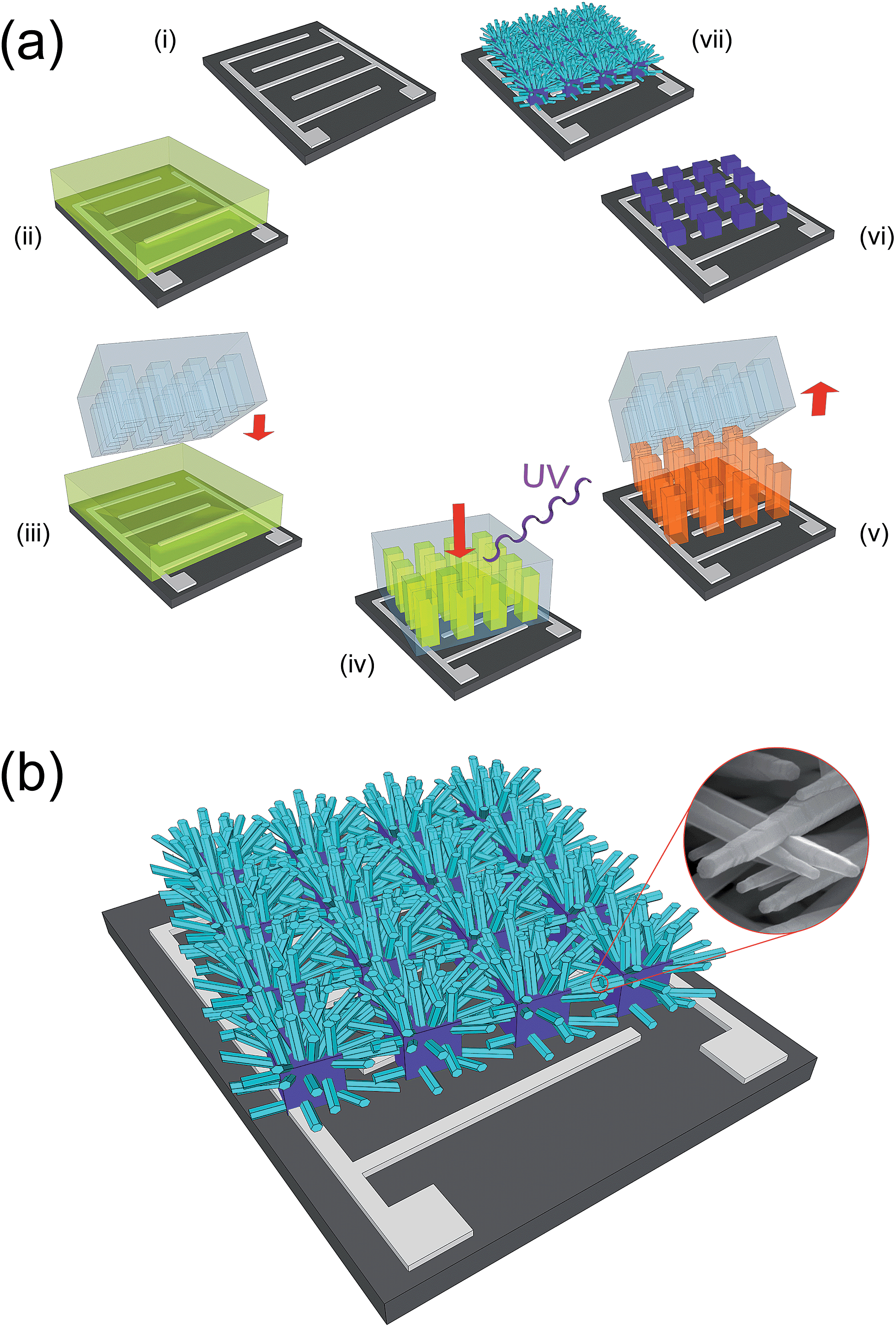 | ||
| Fig. 1 (a) Schematics of the fabrication process for the ZnO NRs network: (ii) deposition of a film of zinc-loaded hydrogel precursor by spin coating; (iii) casting of a PDMS mold; (iv) UV photo-polymerization of the precursor while applying a uniform load over the mold; (v) peeling of the PDMS mold; (vi) thermal degradation of the zinc-loaded hydrogel pattern; (vii) hydrothermal growth of the ZnO NRs. (b) Schematics of a functional device realized by growing the network of NRs on Pt interdigitated electrodes. Inset: SEM micrograph showing details of the bridging NRs. | ||
The same simple procedure can be applied with no modifications on substrates presenting metallic interdigitated electrodes. A schematic of a network of ZnO NRs synthesized on this kind of substrate is shown in Fig. 1b, which highlights how the purpose of providing an electrical path between two electrodes can be efficiently fulfilled by the bi-dimensional network of inter-connected ZnO NRs, grown from neighboring ZnO pillars. The inset of Fig. 1b shows the good contact existing between adjacent NRs.
2.1. Patterning of the seeding layers
As mentioned above, the first stage of the process is represented by the synthesis of the micropillars of nanocrystalline ZnO, which will then act as seeding points for the subsequent growth of the NRs network. The good outcome of this first step, in terms of patterning quality, is therefore crucial for the entire process: Fig. 2 shows the results obtained at this stage of the procedure. After removal of the PDMS mold, a high quality pattern of prisms made out of solid Zn-loaded hydrogels is obtained (Fig. 2a). The base dimensions of the prisms are 3.5 × 3.5 μm, while their height is about 10 μm. The spacing between the prisms was about 6 μm. Upon thermal treatment the organic matrix is degraded and the zinc ions dissolved in the hydrogel convert into ZnO. The process is accompanied by a significant contraction in molar volume. This volume contraction is mostly adjusted through a reduction in the micropillar height, but a significant lateral shrinkage is also observed. Fig. 2b and c show the pattern at the end of the degradation process. Small 1 × 1 × 2 μm pillars of ZnO are observed here. They appear to be slightly deformed as a result of the large volume contraction associated with the process. The pillars are polycrystalline and characterized by a grain size of about 15–20 nm. As a result of the lateral shrinkage produced by the thermal degradation the distance between the micropillars is increased to about 8 μm. The design of the pattern was accurately planned to ensure an efficient electrical contact, once the NRs are grown. Taking into account the lateral shrinkage associated with the degradation process (which was modeled on several patterns with different geometries), we planned a final distance between adjacent pillars of about 8 μm, a dimension comparable with the expected maximum length of our NRs (about 10 μm) and allowing effective bridging between neighboring pillars even in the presence of a significant tilting angle.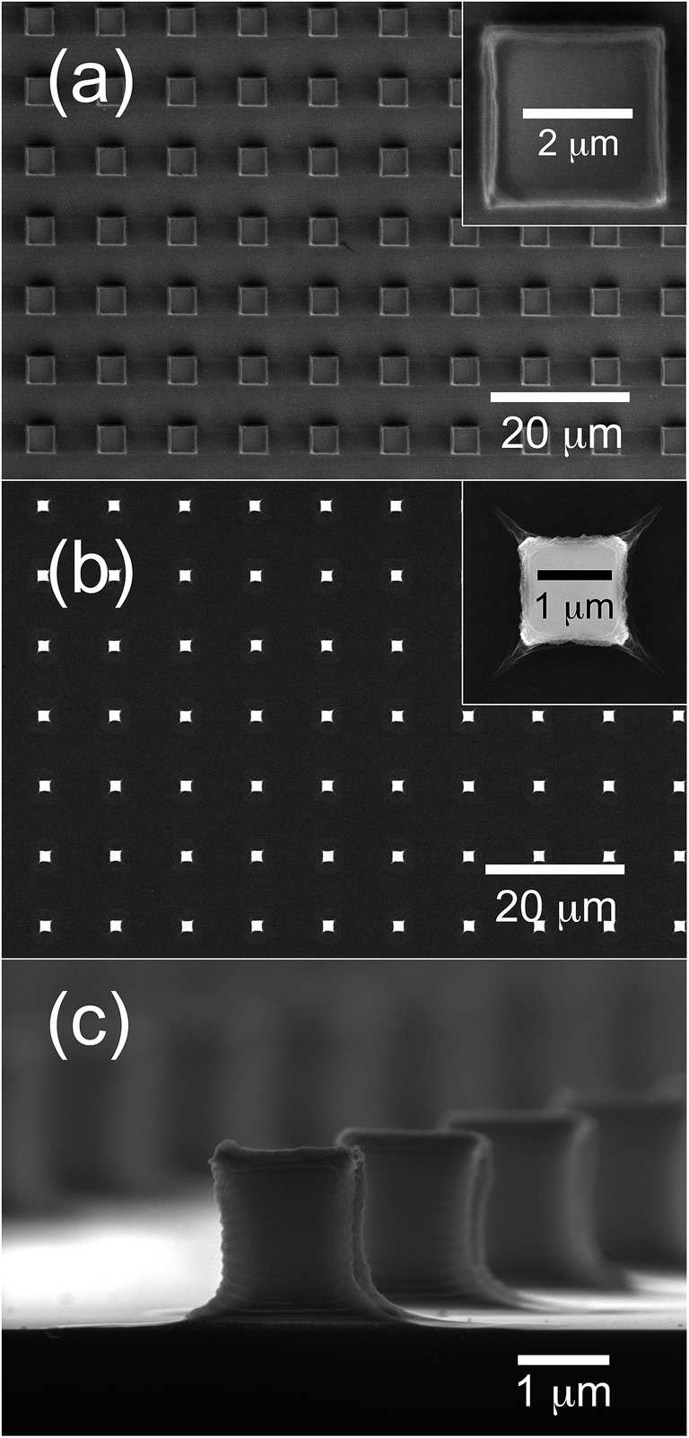 | ||
| Fig. 2 Formation of the ZnO seed micropillars. (a) Top-view of the patterned hydrogel precursor after the soft-lithography process (micromoulding) presenting micro-pillars with a size of about 3.5 × 3.5 × 10 μm; (b) top-view of the same pattern after thermal degradation at 500 °C for 1 h; (c) vertical view of an enlarged image of the ZnO micropillars, obtained after thermal degradation, with dimensions of about 1 × 1 × 2 μm. | ||
Although presenting some slight deformation, the quality of the lithographic process appears to be excellent, despite the large decrease in molar volume associated with the degradation process. The patterns are uniform and defect free over large areas, up to several square millimeters. The complete absence of any residual film between the micropillars even when an inexpensive and untreated microscope glass slide is used as a substrate must also be noted.
2.2. Growth of the ZnO NRs network
The next step of the process is represented by the hydrothermal growth of the network of ZnO NRs. We optimized a hydrothermal synthesis allowing the growth of ZnO NRs with a high length-over-diameter ratio. This synthesis employs zinc nitrate as a source of cations, and hexamethylenetetramine (HMT) as a base in the presence of ammonium hydroxide and polyethylenimine (PEI). Zinc nitrate and HMT are widely employed as sources of Zn2+ and NH3, respectively. The latter serves as a base for the production of OH−, which in turn forms the soluble tetrahedral Zn(OH)4− complex through the reaction Zn2+ + 4OH− ⇌ Zn(OH)4−. Such a complex is involved in the nucleation of ZnO at the interface of the seed-layer grains exposing their (0001) face to the growth solution. This process results in the formation of primordial ZnO NRs through the reaction Zn(OH)4− ⇌ ZnO + H2O + 2OH−.47,48 The growth rates V of the exposed surfaces of ZnO NRs are known to follow the order V (0001) > V (10![[1 with combining macron]](https://www.rsc.org/images/entities/char_0031_0304.gif) 0) > V (10) > V (101); as a result, the primordial NRs tend to grow preferably along their c-axis [0001] over the entire hydrothermal reaction, achieving a large aspect ratio (length/diameter).18
0) > V (10) > V (101); as a result, the primordial NRs tend to grow preferably along their c-axis [0001] over the entire hydrothermal reaction, achieving a large aspect ratio (length/diameter).18
Although ammonia is formed through the hydrolysis of HMT, an additional amount of ammonia has been introduced into the growth solution to help suppress the homogeneous nucleation of ZnO.33,49 Ammonia, in fact, forms complexes with the zinc ions, Zn2+ + nNH3 ⇌ Zn(NH3)n2+ (n = 1, 2, 3, 4), lowering the concentration of free Zn2+ in the solution. Since the homogeneous nucleation of ZnO usually requires a higher level of supersaturation with respect to the heterogeneous nucleation, an accurate choice of the ammonia concentration results in the suppression of homogeneous nucleation, maintaining the possibility of heterogeneous nucleation. The addition of a large amount of ammonia, however, may also cause a decrease of the NRs growth rate due to the resulting decrease in the concentration of free Zn2+. To avoid this effect polyethylenimine (PEI) has been added to the solution. PEI is a well-known organic non-polar surfactant usually added to limit the growth in the width of ZnO NRs by virtue of its tendency to interact preferably with non-polar lateral surfaces of ZnO NRs, reducing their lateral growth.25,26,31 In this case, the presence of PEI helps to limit the growth of the homogeneously formed small nuclei of ZnO by adsorbing onto their surfaces and causing in turn their re-dissolution. This reduces the need for employing high ammonia concentrations.33 The suppression of homogeneous nucleation is of primary importance if long and narrow ZnO NRs need to be grown. In fact, the occurrence of homogeneous nucleation decreases the concentration of Zn2+ in the solution, resulting in a lower growth rate of NRs.
The optimization of the hydrothermal reaction through fine tuning either of the concentrations of the chemicals or of the reaction temperature allowed us to obtain long and narrow ZnO NRs presenting a high aspect ratio (∼100) and a large length of about 10 micrometers. Such morphological features of ZnO NRs obtained allowed filling the distances between different ZnO pillars of the patterned seed-layer as well as the formation of a large number of junctions between NRs in contact with each other, which is required for electrical connection over the network of nanostructures.
Fig. 3 illustrates the very early stages of the process. Fig. 3a shows that the NRs originate from the nanograins that constitute the micropillars and grow perpendicular to their surfaces (Fig. 3b). As the hydrothermal process goes on, both the length and diameter of the NRs are increased, although at very different rates due to the different growth rates of top and lateral surfaces of NRs. The gradual increase in the diameter of NRs appears to be accompanied by a decrease in the density of NRs, indicating the possibility of merging of neighboring NRs during the process. Further evolution is shown in Fig. 4 and 5, which depict respectively the top and cross-section views of the NRs networks grown at zero (a), 135 (b), 180 (c), and 300 min (d). Here a gradual increase in the length (and diameter) of NRs is observed (Fig. 4b–d and 5b–d) until the NR tips come into contact with each other and forming well-developed connections, as can be observed in the micrographs reported in Fig. 6.
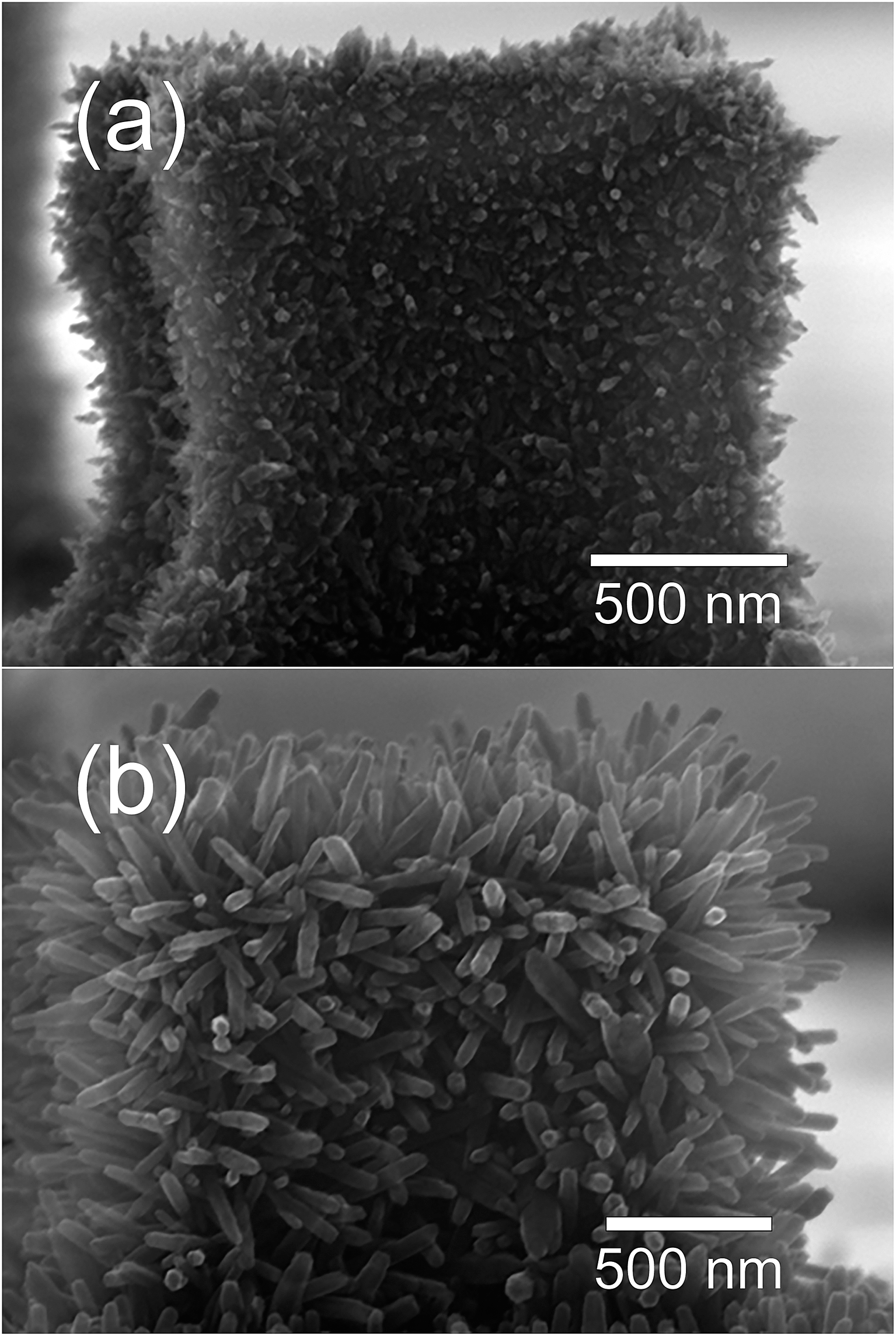 | ||
| Fig. 3 Early stages of the NRs hydrothermal growth on the surfaces of a ZnO micropillar. | ||
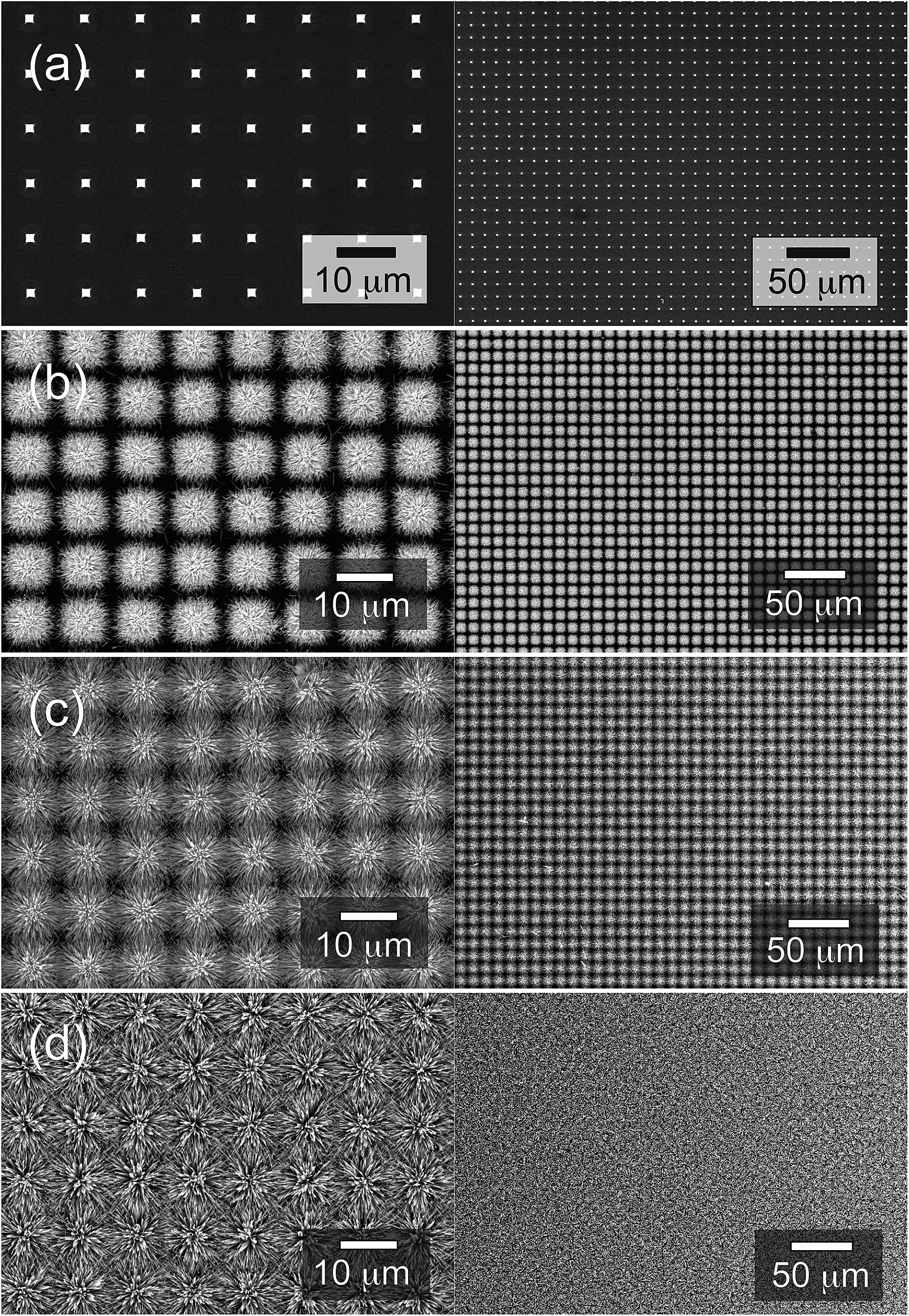 | ||
| Fig. 4 SEM micrographs showing top-views of the NRs growth process at two different magnifications (left side: 3000×, right side: 750×). The images show the patterned ZnO micro-pillars (a) and the ZnO NRs after 135 (b), 180 (c) and 300 min (d) of growth. | ||
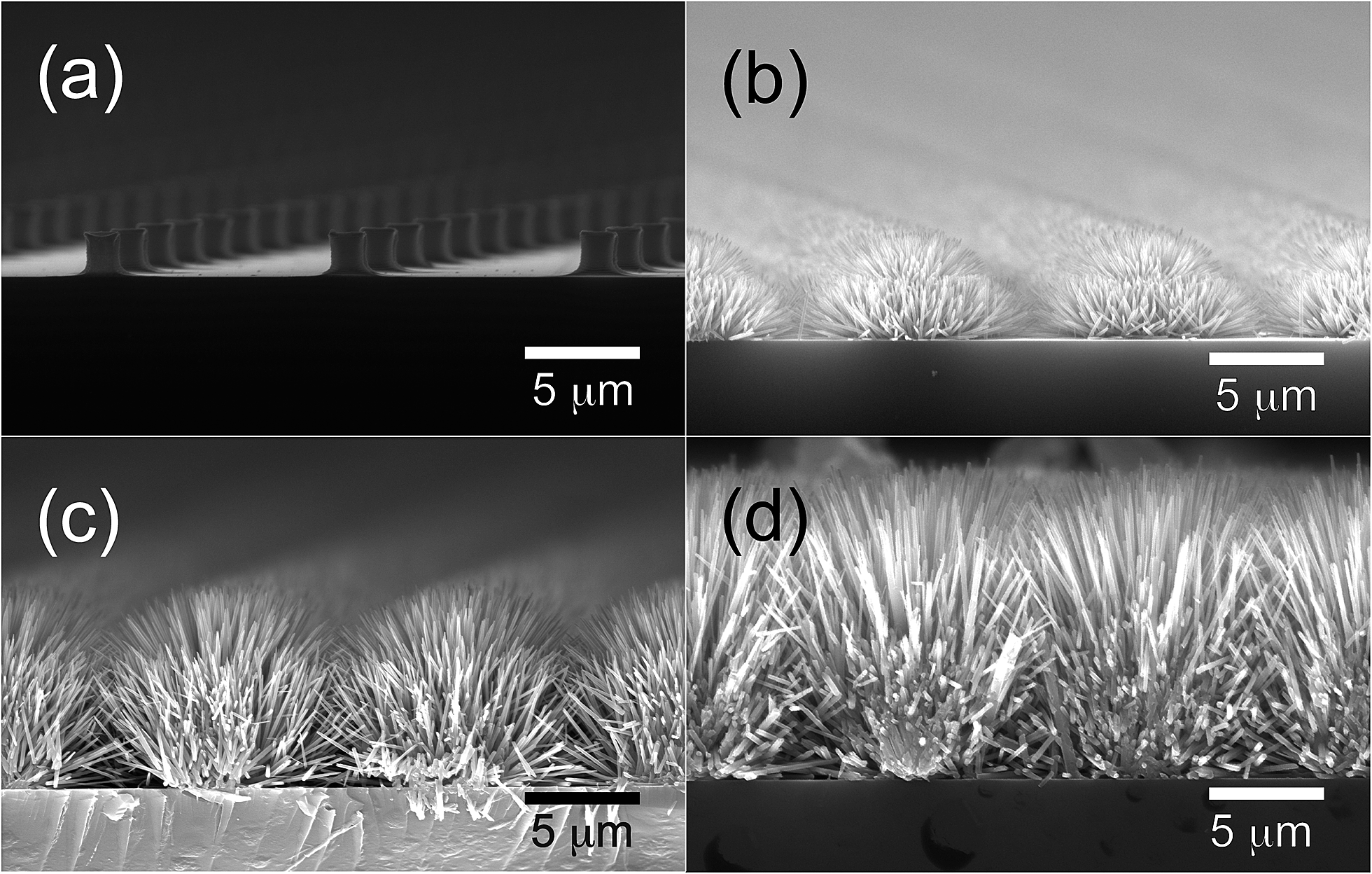 | ||
| Fig. 5 Cross-sections of the same samples of Fig. 4. The images show the patterned ZnO micro-pillars (a) and the ZnO NRs after 135 (b), 180 (c) and 300 min (d) of growth. | ||
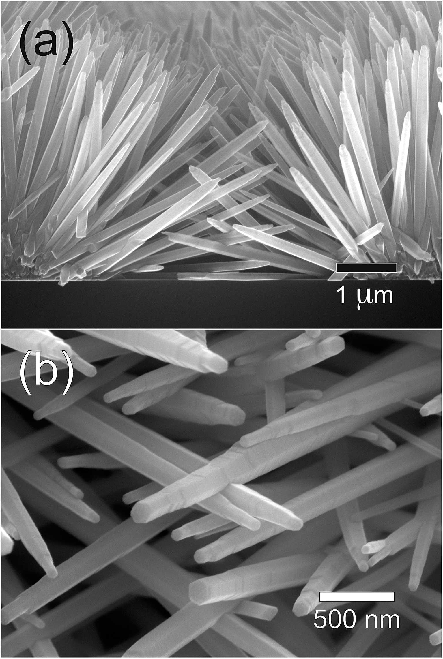 | ||
| Fig. 6 Enlarged views of the samples reported in Fig. 4 and 5 showing the connections between the NRs that grow from neighboring ZnO micropillars: (a) cross-section; (b) top view. | ||
NRs networks characterized by these morphologies have been obtained with excellent uniformity and reproducibility on areas of several square millimeters, as shown in Fig. 4b–d. It must be noted that only NRs originating from the pillars are observed (Fig. 5b–d and 6a) and no growth on the substrate between the pillars is detected at any stage of the process. This ensures that the NR junctions provide the only conduction path existing between the micropillars. As mentioned above, these junctions appeared to be particularly robust; in most cases, in fact, the NRs appear to be intercrossing each other and not just touching on their surfaces (Fig. 6b).50,51
The number of NR junctions appears to increase with the NR length, as can be inferred by comparing the top-views of Fig. 4c and d and the corresponding cross-sectional views of Fig. 5c and d. This observation suggests the possibility that the overall electrical conductivity of the NRs network can be easily controlled through a modification of the parameters that influence the NRs growth, such as the reaction time, the concentration of chemicals and the temperature. Because of these characteristics no further heat treatment is required to improve the conductivity of the NRs network at the end of the process, as often required in the case of networks obtained by the deposition of NRs suspended in a solvent.36,37
The entire deposition process can be reproduced with no modifications on substrates provided with metallic electrodes, allowing the direct realization of actual microdevices (Fig. 7). Fig. 7a shows an example of ZnO seeding micropillars obtained on a silicon nitride substrate presenting interdigitated Pt electrodes. The inset remarks how the lithographic process can produce high quality results independent of the nature of the substrate: the pillar printed across the border between the SiN substrate and the Pt track appears to be perfectly symmetrical and defect-free. A further advantage of this architecture appears evident from the figure: no alignment is required between the electrodes and the micropillars, in order to develop a conduction path. As explained by the schematics reported in Fig. 7b, as long as the distance between the micropillars (A) is smaller than the distance between the Pt lines (B), the formation of a conduction path connecting two lines through a network of ZnO NRs is always possible, regardless of the orientation of the pattern; this is a characteristic that considerably simplifies the realization of an actual device.
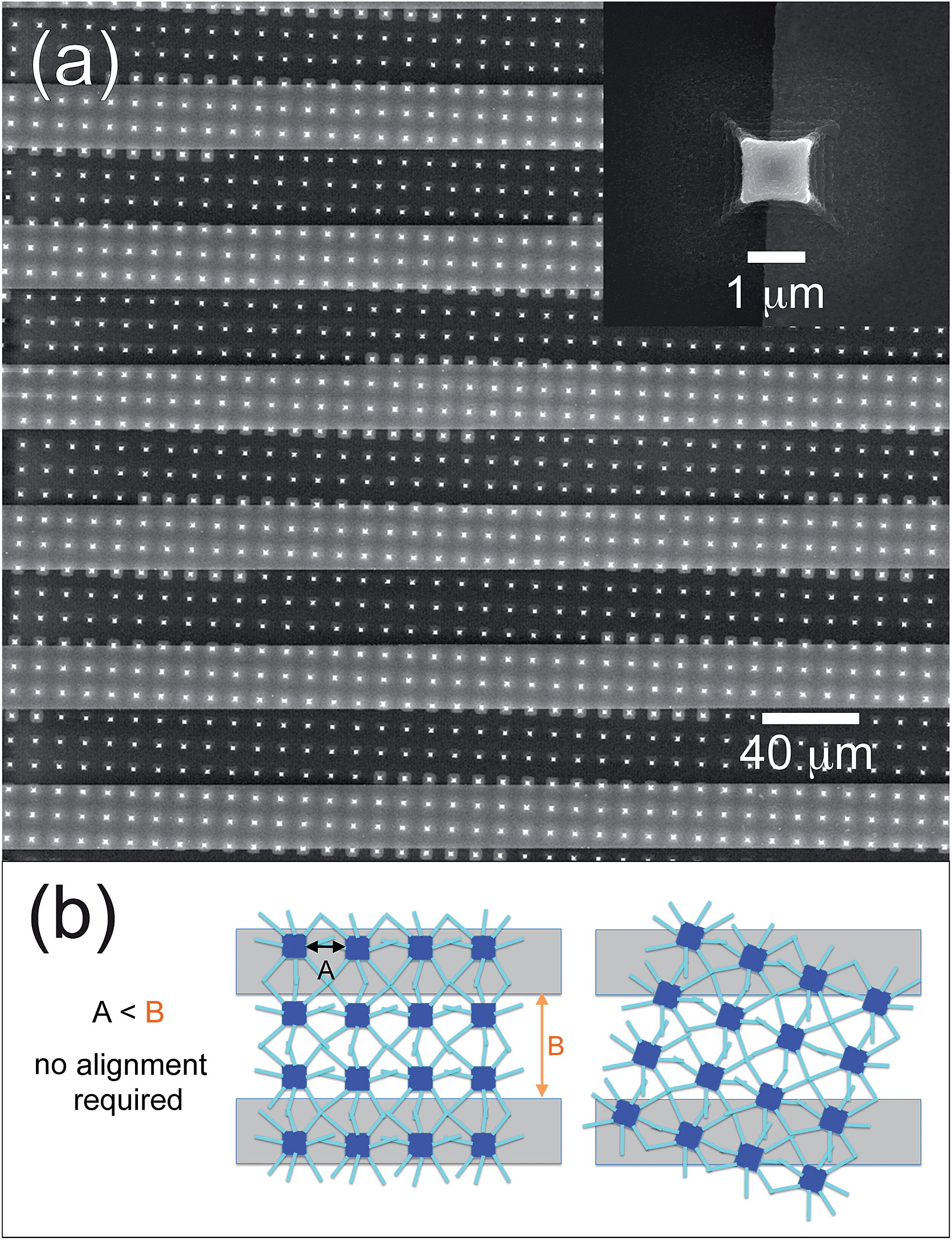 | ||
| Fig. 7 (a) Top-view of a ZnO seeding pattern prepared over Pt interdigitated electrodes: the pattern is not aligned with the electrodes; despite that, a conduction path along the NRs is always possible as long as the distance between the micropillars is smaller than the pitch between the metal lines. Inset: example of a pillar of ZnO deposited across the edge of a Pt line of the interdigitated electrodes. (b) Scheme showing how such a final ZnO NRs network allows the formation of electrical contacts between adjacent electrodes, no matter what is the alignment of the ZnO seed layer patterned through soft-lithography. | ||
2.3. Characterization of the networks of ZnO NRs
Fig. 8a shows the XRD pattern of a fully grown network of ZnO NRs similar to the one reported in Fig. 4d. The pattern shows the well-crystallized nature of the material that presents only the peaks corresponding to the zincite hexagonal crystal structure. The relative intensity of the peaks is substantially altered when compared with a standard powder pattern (reported as a reference in Fig. 8a); the peak corresponding to the basal plane (0002) is strongly enhanced as a result of the preferred orientation of the NRs along the c-axis.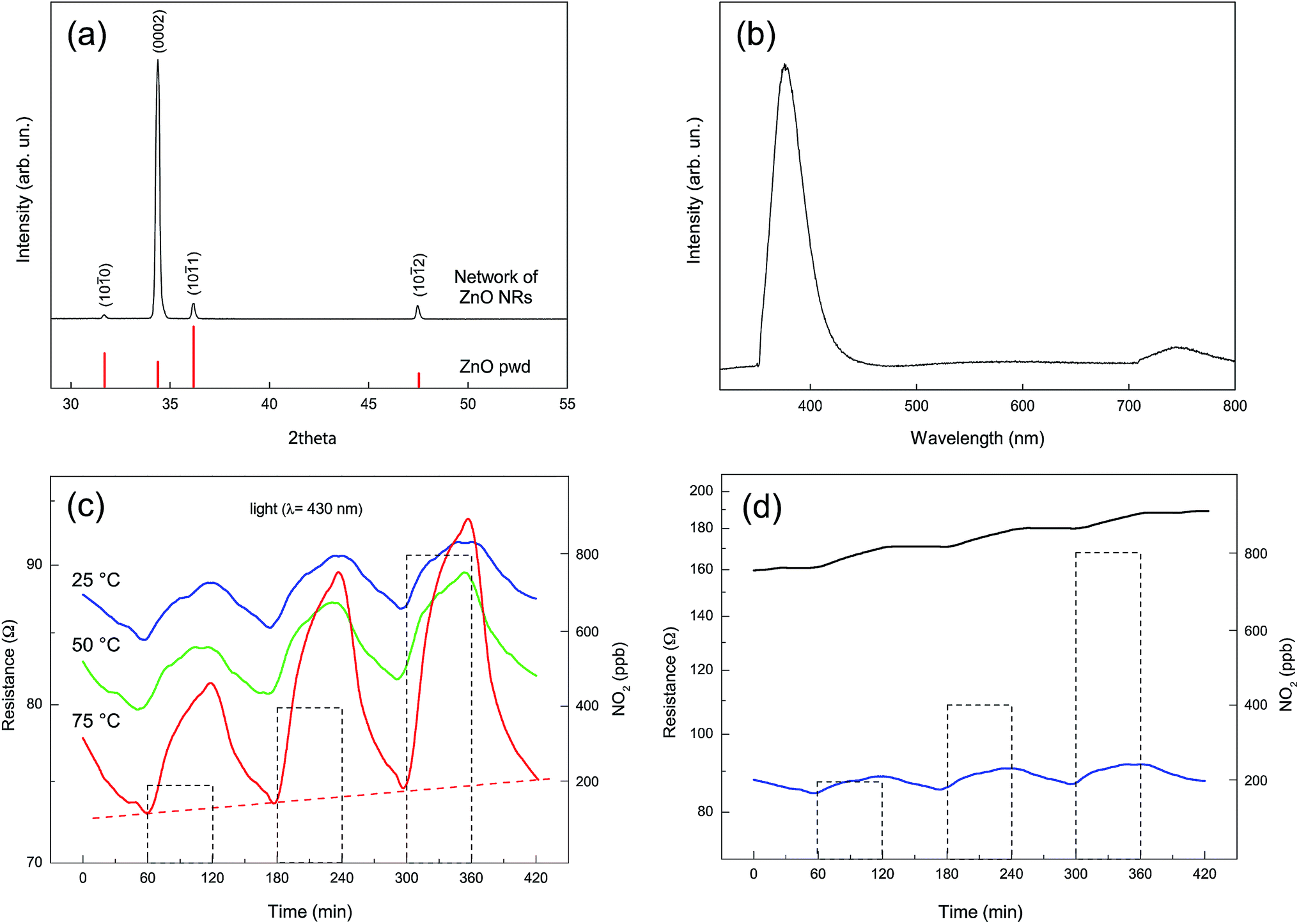 | ||
| Fig. 8 Structural, optical and electrical characterization of an as-grown network of ZnO NRs. (a) X-ray diffraction pattern and (b) room-temperature PL spectrum. (c) Photoelectric-induced resistance modulation at 430 nm purple-blue light wavelength of the ZnO structures at different temperatures. Base line resistance in air at 75 °C is displayed by the red horizontal dashed line. NO2 pulses at 200, 400 and 800 ppb are represented by the vertical dotted rectangular boxes. (d) Room-temperature comparison of the electrical response to NO2 of the ZnO nanostructures, in the dark and under irradiation with 430 nm purple-blue light. | ||
Fig. 8b shows the photoluminescence (PL) spectrum, collected at room temperature, for a typical as-grown NRs network. A major emission peak corresponding to the near-band-edge (NBE) is evident at 380 nm, together with the related small emission signal at twice its wavelength, which is ascribed to the second order diffraction of the NBE emission.52–55 A weak emission band in the visible region between 500 and 700 nm is also evident. This band is usually discussed in terms of overlapping “green” and “orange” components due to oxygen vacancies, surface states, or structural defects.57,58 However, such a visible emission band is only hardly visible in comparison with the UV emission band.59 The absence of this band is generally considered as an indication of the good crystal quality of the ZnO nanostructures.57
With the purpose of testing the presence of electrical connection between the NRs we tested the electrical response of the network derived from its exposure to NO2. Gas concentrations between 200 and 800 ppb and UV irradiation with a light source characterized by a λmax of 430 nm and at different temperatures (25, 50, and 75 °C) have been used (Fig. 8c).
The sensitivity response (SR) of the device is represented by the function SR (%) = [(Rg − Ra)/Ra] × 100, where Rg indicates the network resistance in NO2 and Ra its resistance in air (base line resistance). Table 1 shows the SR at different operating temperatures and different gas concentrations. It is evident that higher operating temperatures result in better values of SR for all the investigated gas concentrations. Several NO2 gas response tests have been carried out and the SR uncertainty is reported in Table 1.
| Temperature | 200 ppb NO2 | 400 ppb NO2 | 800 ppb NO2 |
|---|---|---|---|
| 25 °C | 4.76 ± 1.04 | 6.18 ± 1.67 | 5.75 ± 1.52 |
| 50 °C | 5.59 ± 1.16 | 8.27 ± 1.34 | 9.75 ± 1.73 |
| 75 °C | 11.55 ± 1.53 | 21.4 ± 2.23 | 25.33 ± 3.22 |
Gas adsorption/desorption is reversible, indicating a complete recovery of the base line that appears to be more complete at higher operating temperatures (i.e. 75 °C), as reported in Fig. 8c.
The resistance increase observed upon NO2 exposure confirms an n-type response, in agreement with previous research.60 The surprisingly low resistance in dry air, which ranges between 70 and 90 Ohm when the device is illuminated at a 430 nm wavelength in the 25–75 °C temperature range, provides clear evidence for the occurrence of extended, well developed connections between the bridging self-assembled NRs. These conductivity values are at least two orders of magnitude higher than the one obtained under the same experimental conditions using thin films, nanolines and calcined ZnO powders exposed to UV-LED irradiation.61,62 This feature derives from the peculiarity of the produced nanostructure, composed of well crystallized NRs, presenting a large number of connections and a strong bonding with the electrodes. The overall dimension of the network, that extends without interruptions on the whole surface covered by the interdigitated electrodes (5 × 5 mm), contributes to producing a low baseline resistance. The data from Fig. 8c also indicate that our NRs network is able to recognize the presence of NO2 oxidizing gas at very low concentration values. A quite limited comparison with previously reported devices based on NRs networks can be performed in the case of NO2 gas as a target analyte. Only a few of these devices have been described in the literature41,42,63 and only in two cases the sensing material was ZnO,41,42 but none of these examples involved a low temperature detection in the presence of UV or visible activation.
Under dry air and dark conditions oxygen species such as O2−, O−, and O2− are known to be adsorbed onto the surface of metal oxides, with the latter species being predominant at room temperature.64 The formation of O2−(ads) involves the capture of free electrons in the conduction band through the reaction:
| O2 (phys) + e′ ⇌ O2−(ads) |
A depletion layer is formed at the surface of the metal oxide, which in turn increases the resistance of the sensor. When the oxygen partial pressure or the temperature varies, O2−(ads) may be released forming O2 (phys) or even O2 (gas) and e′. It was suggested that at conventional operating temperatures upon exposure to NO2 gas under dark conditions, the bound electron from the adsorbed oxygen species O2−(ads) might be transferred to the physisorbed NO2 through the reaction:
| NO2 (phys) + O2−(ads) ⇌ NO2−(ads) + O2 (phys) |
When the physisorbed NO2 accepts electrons from O2−(ads), the stable chemisorbed NO2−(ads) state is created. It is well known that NO2−(ads) forms surface acceptor levels deeper than oxygen ion O2−(ads) and increases the thickness of the depletion layer. However, at room temperature under dark conditions, O2−(ads) is stable and NO2 (phys) molecules do not easily extract bound electrons from O2−(ads) to form NO2−(ads).65,66 UV irradiation strongly enhances the chemisorption of NO2 at low temperatures, improving the NO2 sensing response. As it has been suggested, holes and electrons photogenerated through a band-to-band excitation might induce either the release of O2−(ads) or the formation of NO2−(ads), according to the following reactions:
| O2−(ads) + h˙ ⇌ O2 (gas) |
| NO2 (phys) + e′ ⇌ NO2−(ads) |
The strong influence of UV radiation on the sensitivity and response time of semiconducting oxides has been intensively investigated only recently.61,62,66–68 In our case the energy of the radiating source is too low to photogenerate electron–hole couples, as its wavelength (430 nm) is well above the intrinsic absorption edge for ZnO, located at 380 nm. However, recently it has been pointed out that electrons in the valence band of ZnO can be promoted to the conduction band by lower energy photons through two- or multi-photon processes.62 These generated holes can then interact with the chemically adsorbed oxygen molecules, promoting their desorption and producing free adsorption sites for the target molecules. As evidenced in Fig. 8d, however, the resistance of the sample at 25 °C under dark conditions is only twice the resistance of the irradiated sample. This again indicates that the elevated conductivity of our samples is primarily related to the extended interconnectivity between the elements of the NRs network and to their good connection with the Pt electrodes.
3. Experimental section
3.1. Patterning of ZnO seed layers
A polymeric hydrogel precursor was obtained by mixing poly(ethylene glycol)dimethacrylate (PEG-DMA, Mn 550) with a cross-linker (trimethylolpropane benzoate diacrylate), with methanol as a solvent and 2,2-dimethoxy-2-phenylacetophenone as a photoinitiator. Zinc ions were added to the hydrogel by dissolving Zn(NO3)2·6H2O in the precursor solution. The typical precursor mixture contained methanol (30% wt), PEG-DMA (40% wt), trimethylolpropane benzoate diacrylate (8% wt), photoinitiator (10% wt), and Zn(NO3)2·6H2O (7% wt), corresponding to a zinc concentration of 0.30 M. All these chemicals were purchased from Sigma-Aldrich and used as received. The substrates were microscope glass slides, silicon and silicon nitride wafers, some of them were provided with interdigitated Pt electrodes. Before use they were cleaned with acetone (99.8% wt), dried at 200 °C on a hot plate for 5 min. A few drops of the precursor solution were placed on the substrate and then patterned through a soft-lithographic approach using a polydimethylsiloxane (PDMS) mold. The mold was obtained by pouring a previously outgassed mixture with a 10![[thin space (1/6-em)]](https://www.rsc.org/images/entities/char_2009.gif) :1 ratio of elastomer Sylgard 184 and its curing agent (Dow Corning) onto a silicon master and thermally curing it at 60 °C for 24 h. The silicon master presented a pattern of small pillars 5 × 5 μm wide and 10 μm high. It was produced by photolithography on a p-type silicon wafer (500 μm thick). The photolithographic process was performed using an AZ 5214-E resist and a laser writer DWL 66FS (Heidelberg Instruments) operating at 0.4 mW, followed by inductively coupled plasma-reactive-ion etching (ICP-RIE) realized using an SI 500 plasma etcher (Sentech Instruments GmbH) through the Bosch process, using SF6, Ar and C4F8 gases. The preparation of the silicon master was performed only once for each geometry, as a large number of PDMS molds can be replicated from each master. The soft-lithographic procedure was completed by applying a pressure of 100 kPa on the PDMS mold that was left on the substrate overnight. The assembly was then irradiated with UV (λmax = 310 nm) for 20 min, converting the precursor solution into a solid Zn-loaded hydrogel. The pressure was then released and the substrate was heated on a hot plate at 90 °C for 30 min. The PDMS mold was peeled off leaving a pattern of squared pillars of the Zn-loaded hydrogel on the substrate. The hydrogel was then thermally degraded in static air at 500 °C for 60 min producing a pattern of nanostructured ZnO micropillars.
:1 ratio of elastomer Sylgard 184 and its curing agent (Dow Corning) onto a silicon master and thermally curing it at 60 °C for 24 h. The silicon master presented a pattern of small pillars 5 × 5 μm wide and 10 μm high. It was produced by photolithography on a p-type silicon wafer (500 μm thick). The photolithographic process was performed using an AZ 5214-E resist and a laser writer DWL 66FS (Heidelberg Instruments) operating at 0.4 mW, followed by inductively coupled plasma-reactive-ion etching (ICP-RIE) realized using an SI 500 plasma etcher (Sentech Instruments GmbH) through the Bosch process, using SF6, Ar and C4F8 gases. The preparation of the silicon master was performed only once for each geometry, as a large number of PDMS molds can be replicated from each master. The soft-lithographic procedure was completed by applying a pressure of 100 kPa on the PDMS mold that was left on the substrate overnight. The assembly was then irradiated with UV (λmax = 310 nm) for 20 min, converting the precursor solution into a solid Zn-loaded hydrogel. The pressure was then released and the substrate was heated on a hot plate at 90 °C for 30 min. The PDMS mold was peeled off leaving a pattern of squared pillars of the Zn-loaded hydrogel on the substrate. The hydrogel was then thermally degraded in static air at 500 °C for 60 min producing a pattern of nanostructured ZnO micropillars.
3.2. Hydrothermal growth of ZnO NR networks
Networks of ZnO NRs were obtained through hydrothermal processes using the previously obtained ZnO micropillars as seeding points. The solution for the hydrothermal growth was composed of Zn(NO3)2·6H2O (0.25 mM), ammonium hydroxide (650 mM), HMT (0.25 mM), PEI (2.24 mM) and deionized water. The Zn nitrate solution was added drop-wise under continuous stirring to a solution containing the bases. The final mixture was poured into a Duran® GL45 100 ml laboratory glass bottle and the substrate with the patterned ZnO seed-layer was positioned at the bottom. The hydrothermal treatment was carried out at 90 °C for 135, 180 and 300 min. Finally, the substrate was retrieved, rinsed with deionized water and dried at room temperature.3.3. Structural characterization
XRD measurements were performed by using a Bruker D8 Advance diffractometer equipped with a Cu anticathode (λCuKα = 1.541838 Å), operating at 40 kV and 40 mA. A thin film stage and a Soller slit on the diffracted beam were used. XRD patterns were collected using a 6.5° incident angle, with a step of 0.02° and an acquisition time of 5 s per step.3.4. Microstructural characterization
HR-SEM measurements were performed by using a TESCAN MIRA 3 XMU Microscope, operating at 30 kV on samples previously coated with graphite (Cressington carbon coater 108carbon/A).3.5. Optical characterization
Photoluminescence spectra were recorded by exciting the samples with a 355 nm frequency tripled Nd:YAG laser (PowerChip NanoUV 355 by Teem Photonics, maximum power 12 mW) and collecting the emitted light in reflection configuration. The laser beam was focused to a 0.5 mm diameter spot onto the sample surface. A 355 RazorEdge ultrasteep long-pass edge filter by Semrock was used to reject stray light from the laser pump. Finally, the signal was sent to a monochromator (Acton SP-2300, Princeton Instruments) coupled to a liquid nitrogen-cooled silicon CCD (Spec-10, Princeton Instruments).3.6. Electrical characterization
Gas sensing measurements were carried out on samples that have been grown on a 5 × 5 mm SiO2/Si3N4 substrate, presenting on one side 30 μm spaced Pt interdigitated electrodes, patterned onto the Si3N4 surface, and on the other side a Pt resistor acting as a heater. The Si3N4 layer, grown by CVD on a Si 500 μm thick wafer, was characterized by a nanometric roughness of ±2.5 nm, as determined by AFM microscopy. The electrical tests have been carried out at different operating temperatures (25, 50 and 75 °C) by recording the resistance of the NRs network, using a Keithley 2001 multimeter in dry air and in the presence of different NO2 gas concentrations (200–800 ppb range), obtained by diluting NO2 gas (5 ppm in air) with dry air by an MKS147 multigas mass controller (MKS Instruments Inc.). A full colour 10 mm RGB (Kingbright) light-emitting diode set at 430 nm wavelength (purple-blue light) was used as the irradiation source, producing an estimated light intensity of 0.70 mW cm−2 with a 30 mm distance between the light source and the film.4. Conclusions
We presented a new approach towards the synthesis of large-area sensing devices based on a bi-dimensional network of ZnO NRs. This approach is based on an all-solution method that couples a simple soft-lithographic procedure, applied to metal-loaded hydrogels, and aqueous hydrothermal growth of ZnO NRs. It involves the use of an extremely simple experimental setup and very inexpensive and environmentally friendly chemical reactants. The method allows the formation of well connected networks of NRs over areas of several square millimeters and it can be realized directly over a pattern of metal line electrodes, allowing the fabrication of very stable, robust and inexpensive sensing devices. No alignment between the electrodes and the NRs patterns is required, reducing considerably the complexity of microdevice fabrication. The design of the network forces the probing current to flow directly through the NRs, allowing to take full advantage of their sensing capabilities. In the presence of UV irradiation good responses to NO2 at trace levels (<100 ppb) and fast response times have been obtained even at temperatures between 25 and 75 °C.Acknowledgements
This work was supported by the Italian PRIN_09 Project N° 2009ALAX7Y “Sviluppo di materiali con architettura gerarchica per sensori di ossidi di azoto a bassa temperatura per il monitoraggio ambientale”. The authors would like to thank Laboratorio Arvedi (University of Pavia, CISRiC) for the use of the scanning electron microscope.References
- Z. Song, W. Helin, L. Yuhao, W. Wang, L. Hao, W. Haoning, Q. Pingli, Z. Wei and F. Guojia, IEEE Trans. Nanotechnol., 2014, 13, 167–171 CrossRef CAS.
- M. Hussain, A. Khan, M. A. Abbasi, O. Nur and M. Willander, Micro Nano Lett., 2014, 9, 539–543 CAS.
- C. T. Pan, Y. C. Chen, C. C. Hsieh, C. H. Lin, C. Y. Su, C. K. Yen, Z. H. Liu and W. C. Wang, Sens. Actuators, A, 2014, 216, 318–327 CrossRef CAS PubMed.
- D. Cammi, R. Röder and C. Ronning, J. Phys. D: Appl. Phys., 2014, 47, 394014 CrossRef.
- D. V. Quang, K. Do-Il, D. Le Thai, K. Bo-Yeong, H. Byeong-Ung, J. Mi, S. Kyung-Sik, K. Sang-Woo and L. Nae-Eung, Nanoscale, 2014, 6, 15144–15150 RSC.
- H. Muguerra, G. Berthoux, W. Z. N. Yahya, Y. Kervella, V. Ivanova, J. Bouclé and R. Demadrille, Phys. Chem. Chem. Phys., 2014, 16, 7472–7480 RSC.
- Z. Yuan, J. Mater. Sci.: Mater. Electron., 2014, 25, 2248–2252 CrossRef CAS PubMed.
- D. Y. Son, J.-H. Im, H.-S. Kim and N.-G. Park, J. Phys. Chem. C, 2014, 118, 16567–16573 CAS.
- M. Raja, N. Muthukumarasamy, D. Velauthapillai, R. Balasundaraprabhu, S. Agilan and T. S. Senthil, Sol. Energy, 2014, 106, 129–135 CrossRef CAS PubMed.
- J. Dai, C. Xu, J. Li, Y. Lin, J. Guo and G. Zhu, J. Phys. Chem. C, 2014, 118, 14542–14547 CAS.
- J. Kong, S. Chu, J. Huang, M. Olmedo, W. Zhou, L. Zhang, Z. Chen and J. Liu, Appl. Phys. A, 2013, 110, 23–28 CrossRef CAS PubMed.
- Q.-M. Fu, W. Cao, G.-W. Li, Z.-D. Lin, Z. Chen, C.-B. Xu, Y.-F. Tu and Z.-B. Ma, Appl. Surf. Sci., 2014, 293, 225–228 CrossRef CAS PubMed.
- H. Jeong, D. J. Park, H. S. Lee, Y. H. Ko, J. S. Yu, S.-B. Choi, D.-S. Lee, E.-K. Suh and M. S. Jeong, Nanoscale, 2014, 6, 4371–4378 RSC.
- K. V. Gurav, M. G. Gang, S. W. Shin, U. M. Patil, P. R. Deshmukh, G. L. Agawane and M. P. Suryawanshi, et al. , Sens. Actuators, B, 2014, 190, 439–445 CrossRef CAS PubMed.
- J. Y. Kim, S.-Y. Jo, G.-J. Sun, A. Katoch, S.-W. Choi and S. S. Kim, Sens. Actuators, B, 2014, 192, 216–220 CrossRef CAS PubMed.
- S. J. Kwon, J.-H. Park and J.-G. Park, J. Electroceram., 2006, 17, 455–459 CrossRef CAS PubMed.
- M. Law, L. E. Greene, J. C. Johnson, R. Saykally and P. Yang, Nat. Mater., 2005, 4, 455–459 CrossRef CAS PubMed.
- J. Qiu, X. Li, W. He, S.-J. Park, H.-K. Kim, Y.-H. Hwang, J.-H. Lee and Y.-D. Kim, Nanotechnology, 2009, 20, 155603 CrossRef PubMed.
- J. Qiu, X. Li, F. Zhuge, X. Gan, X. Gao, W. He, S.-J. Park, H.-K. Kim and Y.-H. Hwang, Nanotechnology, 2010, 21, 195602 CrossRef PubMed.
- C. Xu, P. Shin, L. Cao and D. Gao, J. Phys. Chem. C, 2010, 114, 125–129 CAS.
- M. Willander, O. Nur, Q. X. Zhao, L. L. Yang, M. Lorenz and B. Q. Cao, et al. , Nanotechnology, 2009, 20(332001), 1–40 Search PubMed.
- J. H. Park, P. Muralidharan and D. K. Kim, Mater. Lett., 2009, 63, 1019–1022 CrossRef CAS PubMed.
- S. Xu and Z. L. Wang, Nano Res., 2011, 4, 1013–1098 CrossRef CAS.
- R. B. Peterson, C. L. Fields and B. A. Gregg, Langmuir, 2004, 20, 5114–5118 CrossRef CAS.
- Q. Huang, L. Fang, X. Chen and M. Saleem, J. Alloys Compd., 2011, 509, 9456–9459 CrossRef CAS PubMed.
- K. H. Tam, C. K. Cheung, Y. H. Leung, A. B. Djurišić, C. C. Ling, C. D. Beling and S. Fung, et al. , J. Phys. Chem. B, 2006, 110, 20865–20871 CrossRef CAS PubMed.
- Q. Li, J. Bian, J. Sun, J. Wang, Y. Luo, K. Sun and D. Yu, Appl. Surf. Sci., 2010, 256, 1698–1702 CrossRef CAS PubMed.
- D. Polsongkram, P. Chamninok, S. Pukird, L. Chow, O. Lupan, G. Chai, H. Khallaf, S. Park and A. Schulte, Phys. B, 2008, 403, 3713–3717 CrossRef CAS PubMed.
- S.-W. Chen and J.-M. Wu, Acta Mater., 2011, 59, 841–847 CrossRef CAS PubMed.
- M. N. R. Ashfold, R. P. Doherty, N. G. Ndifor-Angwafor, D. J. Riley and Y. Sun, Thin Solid Films, 2007, 515, 8679–8683 CrossRef CAS PubMed.
- J. Qiu, X. Li, W. He, S.-J. Park, H.-K. Kim, Y.-H. Hwang, J.-H. Lee and Y.-D. Kim, Nanotechnology, 2009, 20, 155603 CrossRef PubMed.
- M. Law, L. E. Greene, J. C. Johnson, R. Saykally and P. Yang, Nat. Mater., 2005, 4, 455–459 CrossRef CAS PubMed.
- C. Xu, P. Shin, L. Cao and D. Gao, J. Phys. Chem. C, 2010, 114, 125–129 CAS.
- J. R. Morante, Nanotechnology, 2013, 24, 444004 CrossRef CAS PubMed.
- G. Tulzer, S. Baumgartner, E. Brunet, G. C. Mutinati, S. Steinhauer, A. Köck, P. E. Barbano and C. Heitzinger, Nanotechnology, 2013, 24, 315501 CrossRef CAS PubMed.
- M.-Z. Yang, C.-L. Dai and C.-C. Wu, Sensors, 2011, 11, 11112–11121 CrossRef CAS PubMed.
- J. Gong, Y. Li and Y. Deng, Phys. Chem. Chem. Phys., 2010, 12, 14864–14867 RSC.
- S. H. Ko, I. Park, H. Pan, N. Misra, M. S. Rogers, C. P. Grigoropoulos and A. P. Pisano, Appl. Phys. Lett., 2008, 92, 154102 CrossRef PubMed.
- Y. K. Park, H. S. Choi, J.-H. Kim, J.-H. Kim and Y.-B. Hahn, Nanotechnology, 2011, 22, 185310 CrossRef PubMed.
- N. Liu, G. Fang, W. Zeng, H. Zhou, F. Cheng, Q. Zheng, L. Yuan, X. Zou and X. Zhao, ACS Appl. Mater. Interfaces, 2010, 2, 1973–1979 CAS.
- M.-W. Ahn, K.-S. Park, J.-H. Heo, J.-G. Park, D.-W. Kim, K. J. Choi, J.-H. Lee and S.-H. Hong, Appl. Phys. Lett., 2008, 93, 263103 CrossRef PubMed , Da qui: solo nomi journal da abbreviare e rendere corsivi.
- M.-W. Ahn, K.-S. Park, J.-H. Heo, D.-W. Kim, K. J. Choi and J.-G. Park, Sens. Actuators, B, 2009, 138, 168–173 CrossRef CAS PubMed.
- I. G. Tredici, A. Resmini, F. Yaghmaie, M. Irving, F. Maglia and U. Anselmi-Tamburini, Thin Solid Films, 2012, 526, 22–27 CrossRef CAS PubMed.
- I. G. Tredici, F. Yaghmaie, M. Irving, M. B. J. Wijesundara, F. Maglia, E. Quartarone and U. Anselmi-Tamburini, J. Am. Ceram. Soc., 2011, 94, 3171–3174 CrossRef CAS PubMed.
- I. G. Tredici, F. Yaghmaie, M. Irving, M. B. J. Wijesundara, F. Maglia, E. Quartarone, P. Galinetto and U. Anselmi-Tamburini, Thin Solid Films, 2011, 519, 5854–5860 CrossRef CAS PubMed.
- I. G. Tredici, A. Resmini, S. Pin, P. Ghigna, T. Rovetta, M. Patrini, N. Rotiroti, M. Dapiaggi and U. Anselmi-Tamburini, J. Phys. Chem. C, 2013, 117, 25108–25117 CAS.
- V. Consonni, E. Sarigiannidou, E. Appert, A. Bocheux, S. Guillemin, F. Donatini, I.-C. Robin, J. Kioseoglou and F. Robaut, ACS Nano, 2014, 8, 4761–4770 CrossRef CAS PubMed.
- L. E. Greene, M. Law, D. H. Tan, M. Montano, J. Goldberger, G. Somorjai and P. Yang, Nano Lett., 2005, 5, 1231–1236 CrossRef CAS.
- H. Zhang, D. Yang, X. Ma, Y. Ji, J. Xu and D. Que, Nanotechnology, 2004, 15, 622 CrossRef CAS.
- X. Shan, X. Zhang, J. Gao, L. You, H. Xu, J. Xu, D. Yu and H. Ye, J. Phys. Chem. C, 2009, 113, 18014–18019 CAS.
- R. Yang and Z. L. Wang, Solid State Commun., 2005, 134, 741–745 CrossRef CAS PubMed.
- T. Mahalingam, K. M. Lee, K. H. Park, S. Lee, Y. Ahn, J.-Y. Park and K. H. Koh, Nanotechnology, 2007, 18, 035606 CrossRef CAS PubMed.
- C.-A. Lin, D.-S. Tsai, C.-Y. Chen and J.-H. He, Nanoscale, 2011, 3, 1195–1199 RSC.
- T. Shinagawa, S. Watase and M. Izaki, Cryst. Growth Des., 2011, 11, 5533–5539 CAS.
- W. W. Li, W. L. Yu, Y. J. Jiang, C. B. Jing, J. Y. Zhu, M. Zhu, Z. G. Hu, X. D. Tang and J. H. Chu, J. Phys. Chem. C, 2010, 114, 11951–11957 CAS.
- J. Yi, J. M. Lee and W. I. Park, Sens. Actuators, B, 2011, 155, 264–269 CrossRef CAS PubMed.
- Y. Sun, G. M. Fuge and M. N. R. Ashfold, Chem. Phys. Lett., 2004, 396, 21–26 CrossRef CAS PubMed.
- B. Lin, Z. Fu and Y. Jia, Appl. Phys. Lett., 2001, 79, 943 CrossRef CAS PubMed.
- L.-Y. Chen, Y.-T. Yin, C.-H. Chen and J.-W. Chiou, J. Phys. Chem. C, 2011, 115, 20913–20919 CAS.
- S.-W. Fan, A. K. Srivastava and V. P. Dravid, Sens. Actuators, B, 2010, 144, 159–163 CrossRef CAS PubMed.
- S.-W. Fan, A. K. Srivastava and V. P. Dravid, Appl. Phys. Lett., 2009, 95, 142106 CrossRef PubMed.
- Q. Geng, Z. He, X. Chen, W. Dai and X. Wang, Sens. Actuators, B, 2013, 188, 293–297 CrossRef CAS PubMed.
- Y.-J. Choi, I.-S. Hwang, J.-G. Park, K. J. Choi, J.-H. Park and J.-H. Lee, Nanotechnology, 2008, 19, 095508 CrossRef PubMed.
- N. Barsan and U. D. O. Weimar, J. Electroceram., 2002, 7, 143–167 CrossRef.
- H.-J. Lim, D. Y. Lee and Y.-J. Oh, Sens. Actuators, B, 2006, 125, 405–410 CrossRef CAS PubMed.
- C. Zhang, A. Boudiba, P. De Marco, R. Snyders, M.-G. Olivier and M. Debliquy, Sens. Actuators, B, 2003, 181, 395–401 CrossRef PubMed.
- S.-W. Fan, A. K. Srivastava and V. P. Dravid, Appl. Phys. Lett., 2009, 95, 142106 CrossRef PubMed.
- J. T. Yates, Surf. Sci., 2009, 603, 1605–1612 CrossRef CAS PubMed.
| This journal is © The Royal Society of Chemistry 2015 |