
 Open Access Article
 This Open Access Article is licensed under a Creative Commons Attribution-Non Commercial 3.0 Unported Licence
Synthesis of high quality two-dimensional materials via chemical vapor deposition
Jingxue
Yu
,
Jie
Li
,
Wenfeng
Zhang
and
Haixin
Chang
*
Center for Joining and Electronic Packaging, State Key Laboratory of Material Processing and Die & Mould Technology, School of Materials Science and Engineering, Huazhong University of Science and Technology, Wuhan 430074, China. E-mail: hxchang@hust.edu.cn
First published on 3rd August 2015
Abstract
Two-dimensional (2D) materials have attracted much attention due to their unique properties and great potential in various applications. Controllable synthesis of 2D materials with high quality and high efficiency is essential for their large scale applications. Chemical vapor deposition (CVD) has been one of the most important and reliable techniques for the synthesis of 2D materials. In this perspective, the recent advances in the CVD growth of three typical types of two-dimensional materials, graphene, boron nitride and transition metal dichalcogenides (TMDs), are briefly introduced. Large area preparation, single crystal growth and some mechanistic insight are discussed with details. Finally we give a brief comment on the challenges of CVD growth of 2D materials.
 Jingxue Yu | Jingxue Yu is a postdoctoral research fellow at Huazhong University of Science & Technology. He received his BS and doctoral degrees in Materials Science & Engineering at Zhejiang University. Current research interests include synthesis and applications of graphene. |
 Jie Li | Jie Li is a Ph.D. candidate in the Department of Materials Science and Engineering at Huazhong University. He graduated from Shandong University of Technology in 2014. His current research focuses on the preparation and application of two-dimensional materials, especially for transition metal dichalcogenides (TMDs). |
 Wenfeng Zhang | Wenfeng Zhang is currently an associate Professor in the School of Materials Science and Engineering, Huazhong University of Science and Technology (HUST), China. He received his Ph.D. degree from City University of Hong Kong, Hong Kong, China, in 2009. Then he worked in City University of Hong Kong, and the University of Tokyo as a postdoctoral researcher before he moved to HUST. His current research interests focus on post-silicon semiconductor materials and devices, including graphene, transition metal dichalcogenides (TMDs), germanium and III–V semiconductors etc. |
 Haixin Chang | Haixin Chang is a full Professor in the School of Materials Science and Engineering, Huazhong University of Science and Technology, China. He got his Ph.D. in Materials Science in 2007 from the Institute of Metal Research, Chinese Academy of Sciences. Then he worked in the Department of Chemistry, Tsinghua University and the Nanotechnology Centre, ITC, Hong Kong Polytechnic University before moving to Tohoku University in 2011. He was an Assistant Professor in WPI-AIMR, Tohoku University from 2012 to 2014. He received several awards such as the National Thousands Talents Youth Award and the Pulickel M. Ajayan Award. His research covers the broad topics of quantum nanomaterials and devices, with a recent focus on the synthesis, properties, low-dimensional physics, and electronic, optoelectronic and energy applications of graphene, transition metal dichalcogenides (TMDs) and other two-dimensional and quantum materials. |
Introduction
Chemical vapor deposition (CVD) is a time-honored technique that dates back to centuries ago. The first industrial application of the CVD technique can be traced back to 1897 when de Lodyguine1 reduced tungsten hexachloride using hydrogen to deposit tungsten onto the carbon filament of lamps. CVD was then developed as a reliable extraction method to produce highly purified materials such as Ti, Ta, Zr and Si. For example, the Siemens method and its modifications2 are currently applied in the mass production of high-purity polycrystalline silicon, which is vital for the final production of single crystal silicon. Despite the massive application of CVD, it is only in the past half century that the in-depth insight into the process has been achieved.3 CVD has already been recognized as a reliable synthetic method for zero-dimensional nanomaterials (quantum dots and nanocrystals) and one-dimensional nanomaterials (nanowires and nanotubes, etc.).Two-dimensional (2D) materials have attracted much attention due to their unique properties and great potential in various applications. Controllable synthesis of two-dimensional materials with high quality and high efficiency is essential for their large scale applications. The methods for synthesis of two-dimensional materials mainly include mechanical exfoliation, liquid phase routes, and CVD. Mechanical exfoliation of bulk materials is able to acquire final products of the highest quality with very limited efficiency. Liquid phase reactions, such as chemical exfoliation and hydrothermal or solvothermal reactions, have high efficiency but the size of the sheets is usually small and the quality of the product is relatively low and difficult to control compared with mechanical exfoliations. CVD, on the other hand, offers a compromise between quality, efficiency, consistency, and control over the process. The efficiency is much higher than for mechanical exfoliation, and the quality control is better than liquid phase routes. Therefore CVD has been recognized as a reliable route for preparing high quality two-dimensional (2D) materials recently.
Typically, CVD growth of 2D materials involves activated chemical reactions of precursors in a specially-designed environment. The precursors, conditions, atmospheres, substrates and catalysts (if necessary) are several key factors affecting the final quality of the 2D materials. Much progress has been made in preparing 2D materials by CVD and many challenges must be addressed. Herein, we briefly review the CVD growth of several signature layered two-dimensional materials such as graphene, BN, and transition metal dichalcogenides (TMDs), focusing mainly on the precursors, conditions, substrates and end products. The advances in the preparation of large area and single crystal two-dimensional materials are introduced briefly with some discussion of the mechanism, and only a small part of the excellent work to date is included due to the limited space.
CVD growth of graphene
Ever since the first discovery in 2004 and being the subject of the Nobel Prize in physics in 2010,4 graphene has been a point of interest for the scientific community. The first graphene sample was prepared via exfoliation using Scotch tape, which exhibited limited efficiency despite being of the highest quality of all samples made from all the available methods. Other methods have been developed to synthesize graphene in order to improve the efficiency, such as liquid-phase exfoliation, reduction of graphene oxides and bottom-up methods including chemical vapor deposition. Due to the single-atomic thickness of graphene films, the growth of graphene via CVD needs delicate control of the CVD process.As suggested by theoretical modeling analysis and indicated by the experimental results, the mechanism of the catalyzed CVD growth of graphene is similar to the early stage of the catalyzed CVD growth of carbon nanotubes.5,6 The catalyst, however, is in the shape of a film for graphene rather than grains or droplets for carbon nanotubes. With additional manipulation of the reaction parameters, graphene synthesis is favored over that of carbon nanotubes. Transition metals (Cu and Ni),7,8 rare-earth metals (Ru),9 noble metals (Pt)10 and other metals or even compounds have been reported as catalysts for the CVD growth of graphene. Transition metals are believed to be the most efficient catalysts, especially after pre-reaction modification or with certain crystal orientations, and are relatively cheap compared with noble and rare-earth metals.11 Transition metals can work as both synthesizing substrates and catalysts, and are easily removed to obtain free-standing graphene without compromising the integrity of the grown graphene. It should be noted that the CVD growth mechanisms of graphene with Cu and Ni as catalysts are different. Carbon isotope labeling confirmed that the CVD growth of graphene with a Cu catalyst is a surface adsorption process, while the CVD growth of graphene with a Ni catalyst is a diffusion followed by segregation and precipitation process of C on the Ni surface.12
Polycrystalline graphene by CVD
The earliest reports on CVD synthesized thin graphite materials are from the 1970s in the early days of investigation into the CVD process.13–15 However, the first successful synthesis of few-layer graphene films of about 30 layers via CVD was reported by Somani et al. with nickel foils as substrates and camphor as a gaseous reactant (Fig. 1a).8 This work demonstrated the plausibility of the CVD growth of layered graphene films, but there is much room for further reducing the thickness. Following this work, many efforts have been made to optimize the CVD growth of graphene films, focusing on precursors, substrates, catalysts, temperatures and atmospheres. Reina et al. managed to reduce the thickness of CVD synthesized graphene to the few-layer level.16 500 nm Ni film was evaporated onto SiO2/Si substrates as a catalyst. After reductive annealing, few-layer graphene was deposited onto the substrates at 900–1000 °C with 5–25 sccm methane and 1500 sccm hydrogen as the gas flow at atmospheric pressure. The synthesized graphene consisted of 1–12 layers with single or double layer regions of up to 20 μm. The prepared graphene film could withstand multiple processing steps without compromising the structural integrity. In another work, Pollard et al. demonstrated CVD growth of single-layer graphene on a Ni thin film evaporated on SiO2/Si substrates.17 The Ni film was deposited onto SiO2 (300 nm in thickness)/Si(100) substrates by sublimation under 10−4–10−5 Pa. Freestanding single-layer graphene films were obtained by etching off the Ni film.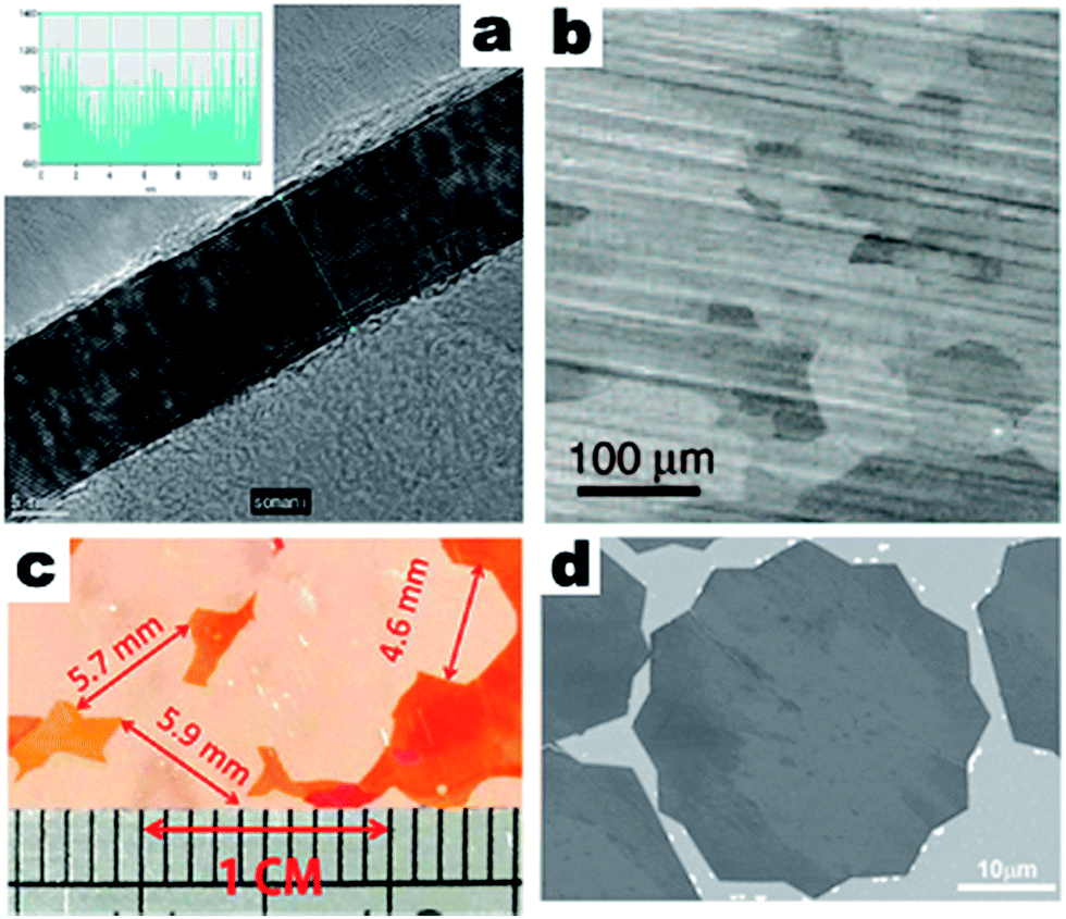 | ||
| Fig. 1 (a) TEM image and intensity pattern along the marked line (inset) of a CVD synthesized graphene film, reprinted from ref. 8 by permission of Elsevier; (b) SEM image of a CVD synthesized single layer graphene film, reprinted from ref. 18 by permission of American Association for the Advancement of Science; (c) optical image of CVD synthesized single graphene sheets on copper foil, reprinted from ref. 36 by permission of American Chemical Society; (d) SEM images of CVD synthesized single crystal twelve point graphene grains on melted copper, reprinted from ref. 43 by permission of John Wiley & Sons. | ||
One of the most important advances in the CVD growth of single layer graphene was reported in 2009. Li et al. prepared large-area graphene films via CVD on copper foils,18 and the grown graphene films were mostly of single-layer thickness, with less than 5% double or triple layers (Fig. 1b). Methane and hydrogen were applied as gas sources in this work, and copper foil substrates were sequentially removed by treatment with iron nitrite solution to obtain free-standing graphene films. The chemical etching process to remove the substrates became widely applied, since it took advantage of the chemical stability of graphene which avoided defects induced by micromechanical exfoliation and enabled easy transfer to dedicated substrates or films for heterostructure construction. To obtain uniform monolayer large area graphene, it is useful to selectively remove the bi-/tri- layer graphene. Fang et al. demonstrated that bi-/tri-layer graphene was selectively removed by the carbon-absorbing W foil enclosed in Cu foil while the monolayer graphene remained intact.19
Compared to single-layer graphene, bilayer graphene has a tunable bandgap which could benefit many electronic and optical device applications.20 Lee et al. prepared wafer-scale bilayer graphene using CVD with methane.21 The key factor in this work was to control the cooling rate down to approximately 18 K min−1. The bilayer coverage was 99%, and the method was easy to scale up. Another route to synthesize bilayer graphene is through the epitaxial growth of one layer graphene onto another layer. Yan et al. demonstrated a layer-by-layer vapor phase epitaxial synthesis of bilayer graphene.22 A second layer of graphene was grown on copper foil which was already deposited with a layer of graphene. However, only 67% coverage of bilayer graphene was achieved and more efforts are needed.
Besides single or bilayer graphene, it is also important to gain control over the number of layers in CVD grown graphene. Gong et al. controlled the number of layers of CVD graphene to within 1–10 layers mainly by controlling the flow of hydrogen, the thickness of the deposited nickel catalyst, and the growth temperature and time.23 But to obtain uniform graphene with a consistent number of layers is still challenging. In another work, by delicately controlling the parameters including temperature, deposition time, overall gas flow and pressure, control over the layers of CVD grown graphene was realized. Tu et al. took the control one step further with an accuracy of down to one single layer within 7 layers.24
For the catalyzed CVD growth of graphene, complicated transfer from metal to working substrates is needed. Therefore, many efforts have been made to deposit graphene films onto the real working substrates without any catalysts. Shang et al. applied microwave-assisted plasma chemical vapor deposition (MPCVD) to grow multi-layered graphene on silicon substrates.25 Hwang et al. synthesized single layer graphene on sapphire substrates via van der Waals epitaxy using CVD.26 Although the deposition temperature was around 1400 °C, p-type and n-type single-layer graphene could be obtained by altering the partial pressure of methane gas. Wang et al. showed a slightly different method and single layer graphene films were synthesized via CVD on h-BN films grown using CVD on copper foils.27 Chen et al. demonstrated catalyst-free CVD growth of single crystal graphene on various dielectric substrates, such as Si3N4/SiO2/Si and sapphire.28 The CVD growth was near-equilibrium, resulting in single crystal graphene sheets with a quality close to that of metal-catalyzed sheets but with a small sheet size of only 11 μm.
Single crystal graphene by CVD
Most of the CVD synthesized graphene is polycrystalline graphene which shows a much inferior performance compared to that exfoliated from bulk graphite. It is believed that the grain boundaries in polycrystalline graphene are the main cause for the inferiority. Thus, many efforts have been devoted to the controllable and high-quality synthesis of single crystal graphene. The common approach is to modify the substrates/catalyst films, typically by annealing under a hydrogen atmosphere at a higher temperature, to promote grain growth and suppress normal CVD growth. Larger grains will induce fewer grain boundaries and thus enhanced performances. Applying single crystal substrates/catalyst films in the CVD growth of graphene would produce single crystal graphene,29 although the commercially-available single crystal substrates/catalyst films are too expensive for wide application.Recently, CVD growth of single crystal graphene was successfully executed on commercial transition metal substrates like copper foils. Vlassiouk et al.7 grew large single crystal graphene via a CVD process under an atmosphere of hydrogen, methane and argon with copper foils as substrates and catalysts, and hydrogen as a cocatalyst. By altering the partial pressure of hydrogen and methane, well-defined perfect single crystal graphene was obtained. The size of the obtained graphene was around 10 μm, and the graphene showed weak binding to the copper foil substrates, which benefitted sequential removal of the substrates and the fabrication of prototype devices. In another work, Wu et al.30 managed to increase the efficiency of single crystal graphene on copper foils made via the CVD method by employing PMMA dot arrays onto the copper foils. The PMMA patterns were sequentially spin-coated, cured and annealed prior to a high temperature CVD process under an atmosphere of argon, methane and hydrogen. By employing additional PMMA coating after the CVD process, the arrangement of the graphene grains was successfully kept uncompromised during the removal of the copper foils and the transfer process. The size of the graphene grains was also around 10 μm. Similarly, under atmospheric pressure, Robertson31 and Warner synthesized hexagonal single crystal graphene domains via CVD with copper as the substrate and hydrogen as the co-catalyst. The obtained graphene was single crystal few layer graphene.
Besides the efficiency, increasing the size of the grown graphene sheets is also a point of interest. Li et al.32 further improved the above-mentioned technical routes one step further. With low pressure and an extended growth time for the CVD process, Li et al. obtained graphene grains as large as 0.5 mm. Copper enclosures were used as substrates, offering a large deposition site for graphene. Wang et al.33 also prepared single crystal graphene sheets with sub-millimeter size via an atmospheric pressure CVD (APCVD) process. Chen et al. suppressed the evaporation loss of copper during the CVD growth of single crystal graphene, and obtained graphene sheets with sizes up to 2 mm.34 In their work, the CVD process was operated under low pressure, and if the deposition process lasted long enough, the copper substrate could suffer from evaporative loss during the deposition due to the high deposition temperature. Controlling chamber pressure can lead to single crystal CVD growth. Yan et al.35 obtained single crystal graphene sheets with a size of 2.3 mm via a controlled chamber pressure CVD process. The chamber pressures of the substrate and catalyst pre-deposition treatment, deposition and cooling procedure were all modified. Besides controlling the chamber pressure, manipulating the carbon source could also trigger the growth of large size single crystal graphene. Gan et al.36 prepared even bigger single crystal graphene sheets by delicately controlling the hydrogen flow throughout the process. The crucial step was to anneal the copper substrates under an Ar atmosphere before the reductive pre-deposition treatment under an Ar/H2 atmosphere. The annealing induced mild oxidation, which provided unique nucleation sites or seeds for the CVD growth of single crystal graphene. With a prolonged deposition time, single crystal graphene sheets with sizes up to 5.9 mm were obtained (Fig. 1c). Zhou et al. also demonstrated similar results.37 They systematically studied argon atmosphere annealing before reductive heat treatment, low chamber pressure and high hydrogen/methane molar ratios of over 1000, and showed significantly reduced nucleation density in the CVD process. The size of the resulting single crystal single-layer graphene sheets was 5 mm, and the size of the resulting single crystal double-layer graphene sheets was 300 μm. These works were all carried out on metal substrates. However, Lee et al. prepared wafer-scale monolayer single crystal graphene on epitaxial Ge films on silicon wafers as a substrate.38 The single crystal monolayer graphene could reach a wafer size of 2 inches.
The carbon precursor applied in the above-mentioned works is gaseous methane, but it is not the only option. Wu et al. demonstrated that, by heating polystyrene with a halon lamp, the carbon source feedstock could easily be manipulated. Even with an atmospheric pressure CVD process, single crystal graphene with sizes up to 1.2 mm could be synthesized.39 This work not only demonstrated the plausibility of modifying the carbon source feedstock to obtain large single crystal graphene, but also revealed a new type of precursor other than gaseous methane. Xue et al.40 also reported the CVD growth of single crystal graphene with pyridine as a precursor, which lead to nitrogen doping during the synthesis. These kinds of CVD growth methods with non-gaseous precursors have the advantage of a significantly lower deposition temperature, but high-temperature pre-deposition treatments of substrates/catalysts are still necessary. Meanwhile, a direct indication and a precise control of the precursor flow is difficult to come by. Therefore, gaseous precursors like methane are still the most applied carbon sources in the synthesis of single crystal graphene using CVD.
Most CVD processes need to be carried out at a temperature below the melting point of copper. However, several works have used a CVD reaction temperature above the melting point of copper, which would favor the growth of relatively large sheets of single crystal graphene. Wu et al.41 raised the deposition temperature to above the melting point of copper, and with Mo foils that could be wetted by copper as the substrates and melted copper as the catalyst, sub-millimeter size single crystal graphene sheets were obtained via atmospheric pressure CVD. Geng et al. demonstrated the CVD growth of smaller but denser single crystal graphene flakes. In their work, control over the size and efficiency of single crystal graphene flakes was gained by controlling the temperature and partial pressure of the methane gas flow.42 Geng et al. demonstrated the controlled CVD growth of twelve pointed graphene grains (TPGGs) on a melted copper film with tungsten foils underneath as substrates (Fig. 1d).43 The as-synthesized TPGG was a single crystal, and the morphology was controlled by altering the carbon feedstock. Melting and resolidifying the substrates prior to CVD growth would achieve a similar effect as keeping the substrates molten. Mohsin et al. melted and resolidified copper film on tungsten substrates by sequentially raising and reducing the temperature to obtain a smooth surface and minimal surface irregularities.44 The nucleation density was significantly reduced and the CVD growth of graphene on this type of copper under a high reaction temperature produced millimeter sized single crystal graphene flakes with well defined hexagonal shapes. The reductive treatment of copper was still necessary to suppress other irregularities in the copper catalyst.
Most single crystal graphene synthesized via CVD is single layer, especially those of a large size. CVD growth of large few-layer single crystal graphene is still a challenge. Yan et al. demonstrated the CVD growth of double and triple layer graphene single crystals, in which the interlayer rotation within graphene single crystals was induced by graphene nucleation steps on the copper foils during the synthesis.45 The pre CVD treatments were prolonged to 7 hours in order to achieve the required copper surfaces. In Table 1, we summarize the substrates, catalysts, overall gas flows, temperatures, pressures and corresponding product qualities of graphene for some typical CVD growth processes.
| Precursor | Special pre-deposition treatment of substrates | Substrates | Metal catalyst | Growth condition | Atmosphere & gas flow | Morphology | Properties | Remarks |
|---|---|---|---|---|---|---|---|---|
| Camphor | N/A | Ni | Ni | 700–850 °C | Atmospheric pressure, Ar | Multi layer graphene film | N/A | Ref. 8 |
| Methane | 60 minutes, 40 mTorr, 2 sccm H2, 1000 °C | Cu | Cu | 1000 °C, 30 min | ∼500 mTorr, 2 sccm H2, 35 sccm CH4 | Single layer graphene films with no more than 5% of domains double or triple layered | Carrier mobility ∼ 4050 cm2 V−1 s−1 | Ref. 18 |
| Methane | 900 W nitrogen plasma 40 Torr several min | Si | N/A | Over 1000 °C, 900–1300 W microwave | 40 Torr, 10–40% methane in N2 | Multi layer graphene film | Fast electron-transfer, selective electrocatalysis | Ref. 25 |
| Methane | N/A | Sapphire | N/A | 1450–1650 °C, 45 s–5 min | 600 Torr, ∼10![[thin space (1/6-em)]](https://www.rsc.org/images/entities/char_2009.gif) 000 sccm Ar, 5–200 sccm CH4, H2:CH4 = 5–15 000 sccm Ar, 5–200 sccm CH4, H2:CH4 = 5–15 |
Single layer graphene films | Carrier mobility ∼ 2000 cm2 V−1 s−1 | Ref. 26 |
| Methane | 1180 °C, 30 min, 250 sccm H2, 300 sccm Ar | Various dielectric materials | N/A | 1180 °C, 2 h | Atmospheric pressure CH4:H2 = 1.9 ∼ 2.3:50 sccm |
Single crystal hexagonal and dodecagonal up to 11 μm | Carrier mobility 5000 cm2 V−1 s−1 | Ref. 28 |
| Methane | 1040 °C, 10 minutes, 700 sccm H2 | Pt(111) | Pt | 1040 °C, 4 h | Atmospheric pressure, 4 sccm CH4, 700 sccm H2 | Single crystal hexagonal graphene sheets of 1 mm | Carrier mobility 7100 cm2 V−1 s−1 | Ref. 29 |
| Methane | Chemical polishing, mild oxidation followed by reductive heat treatment | Cu | Cu | 1050 °C, up to tens of hours | Atmospheric pressure, 15 sccm 500 ppm CH4 diluted in argon, 21 sccm H2 | Single crystal hexagonal graphene sheets of up to 5.9 mm | N/A | Ref. 36 |
| Polystyrene, evaporated | Mechanical & chemical polishing, followed by reductive heat treatment | Cu | Cu | 950–1050 °C, 30–80 min | Atmospheric pressure, 300 sccm overall gas flow of Ar and H2, 0–10 sccm H2 | Single crystal hexagonal graphene sheets of up to 1.2 mm | Carrier mobility 5000–8000 cm2 V−1 s−1 | Ref. 39 |
| Pyridine, bubbled | Reductive heat treatment | Cu | Cu | 300 °C, 0.5–5 min | Atmospheric pressure, H2:Ar = (150:30100:20, 50:10) sccm |
Single crystal tetragonal graphene sheets | Nitrogen doped, carrier mobility 53.5–72.9 cm2 V−1 s−1 | Ref. 40 |
| Methane | Reductive heat treatment | Melted Cu on W | Cu | 1120 °C, 3–5 min | Atmospheric pressure, CH4:H2 = 3–5:300 sccm |
Single crystal twelve pointed graphene sheets | Carrier mobility 2000–5000 cm2 V−1 s−1 | Ref. 42 |
| Methane | Melting and resolidifying under reductive atmosphere | Resolidified Cu on W | Cu | 1075 °C, 5 h | Atmospheric pressure, CH4:H2:Ar = 46:100:854 sccm |
Single crystal hexagonal graphene sheets of ∼1 mm | N/A | Ref. 44 |
| Methane | Reductive heat treatment followed by oxygen exposure | Oxygen-rich Cu | Cu | 1035 °C, 30 min | CH4, 5 × 10⁻³ Torr H2, 0.1 Torr | Multi-branched graphene domains | Carrier mobility 15000–30000 cm2 V−1 s−1 at room temperature |
Ref. 47 |
Mechanistic insight into the CVD growth of single crystal graphene
CVD growth of single and polycrystalline graphene are two procedures that are similar in many aspects (Fig. 2a).35 However, there are several key factors that distinguish the CVD growth of single crystal graphene.46 First, the suppression of nucleation allows space for the growth of single crystal graphene. The pre-deposition, reductive treatment of typical substrates (copper) eliminates impurities, oxides, sharp wrinkles, defects and other structures of the substrates that could favor the nucleation of graphene. Second, by reducing the partial pressure of methane gas in the overall gas flow, the concentration of carbon precursors would be low enough to favor the growth of graphene single crystals over nucleation. Third, the deposition parameters can be controlled so the single crystal graphene grains grow to a relatively large size, but not too large to stack over one another. The parameters include chamber pressure, temperature, heating and cooling discipline, deposition time and composition and flow rate of the overall gas flow.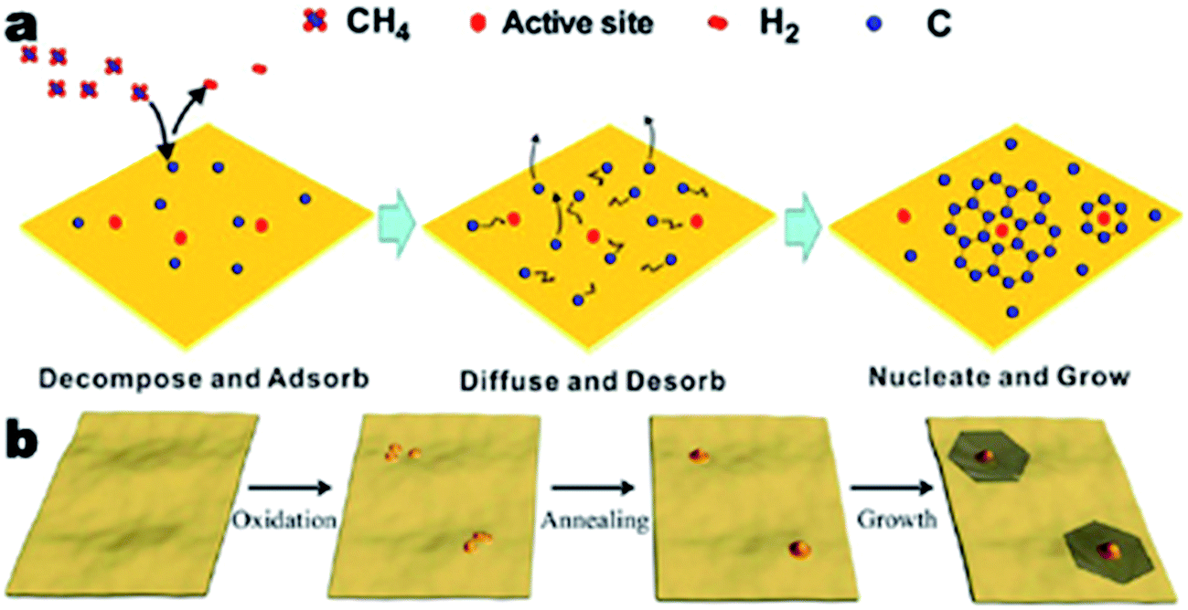 | ||
| Fig. 2 Schematic illustration for the growth mechanisms of the CVD growth process of graphene. (a) CVD growth process with a methane precursor, reprinted from ref. 35 by permission of American Chemical Society; (b) scheme of the mild oxidation and sequential reductive heat treatment before the CVD process, reprinted from ref. 36 by permission of American Chemical Society. | ||
Many investigations indicate the special role of oxygen in the CVD growth of single crystal graphene. Gan et al.'s work showed that by mild oxidation of the copper substrate before reductive annealing, copper nanoparticles of the proper size could be obtained (Fig. 2b).36 The nanoparticles promoted nucleation and growth of large single crystal graphene sheets. In their work, the origin of the oxidation was identified as the trace amount of oxygen in the Ar gas flow or residual oxygen in the CVD chamber. A detailed investigation into the effect of oxygen during the CVD growth of graphene was performed by Hao et al. (Fig. 3).47 Various concentrations of surface oxygen in copper substrates were realized by purchasing copper foils with different purities, altering the hydrogen pressure during the reductive treatment and exposure to pure oxygen before the CVD growth. The studies showed that the surface oxygen in the copper substrates could decrease the concentration of the copper active sites by passivation, and thus suppress nucleation, favoring the growth of single crystal graphene nanosheets. Magnuson et al. offered a new perspective on the role of oxygen and the oxidation process of the copper substrates.48 By intentionally oxidizing the copper substrates, a layer of copper oxides was formed, which would decompose during the following annealing and CVD processes and the residual carbon of the substrates would be eliminated. This kind of behavior was referred to as “self-cleaning”. There is also an excellent study of the in situ observation of the CVD growth of graphene.49 However, a deeper understanding of oxygen in the process is still needed to understand the complete role and mechanism of oxygen and to achieve delicate control over the condition of oxygen.
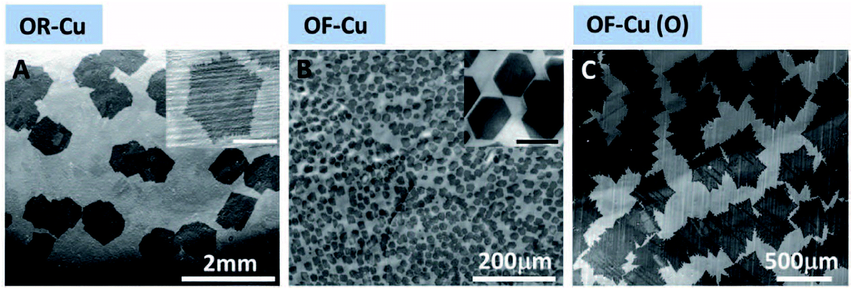 | ||
| Fig. 3 The effect of O on graphene nucleation density and domain shapes on various types of Cu substrates. OR-Cu (A) represents low-purity copper substrates, OF-Cu (B) represents high-purity copper substrates, and OF-Cu (O) (C) represents high-purity copper substrates exposed to oxygen before the CVD growth of graphene. Reprinted from ref. 47 by permission of American Association for the Advancement of Science. | ||
CVD growth of 2D boron nitride (BN)
Group III–V compound thin films have been the focus of artificially-synthesized thin-film materials. Since the 1970s, GaAs thin films have been widely studied via molecular beam epitaxy. Other group III–V compounds such as BN have also attracted much interest from the scientific community. For crystalline BN, there are two types of crystallinity, cubic and hexagonal, designated c-BN and h-BN. C-BN exhibits several fascinating properties, with a hardness second only to that of diamond, high thermal conductivity, high chemical stability and a wide bandgap. In the early research into crystalline BN, much effort was focused on c-BN. H-BN is a relatively new type of material, consisting of sp2-bonded hexagons like graphite. H-BN exhibits a high electrical resistivity, high thermal conductivity, extremely low dielectric constant and outstanding lubrication and anti-corrosion properties. It is vital to effectively control the crystallographic phase of the obtained BN films, which could benefit future applications. However, due to the high cost of molecular beam epitaxy BN, CVD is introduced to lower the cost and promote the widespread production. BN is very suitable for CVD growth since the precursors of B and N are mostly gaseous sources.Pieson's work is among the earliest studies on synthesizing BN via CVD.50 The deposition was carried out in a vertically set CVD device, using BF3 and NH3 as precursors of B and N, respectively. The deposition took place on BN felt fiber substrates at temperatures of 1100 °C to 1200 °C, demonstrating the plausibility of synthesizing BN via CVD. However, BN was deposited homogeneously on the BN substrates, limiting the applications of CVD BN. For heterogeneous synthesis, Yamaguchi et al. demonstrated CVD grown BN on non-BN substrates for the first time.51 In detail, comparative stoichiometric BN films were grown on InP substrates via CVD using B2H6 and NH3 as precursors of B and N, respectively. By introducing PH3 into the overall gas flow, the doping of BN with P was also realized. P-doped BN films on InP substrates were readily applied as gate insulation. Similar work by Nakamura et al. showed that the composition of the BN films synthesized by CVD could be closely controlled by varying the partial pressures of the respective gaseous precursors.52 In addition, various routes of CVD growth to obtain BN were demonstrated, including MOCVD53 with (C2H5)3B and NH3 gaseous precursors, microwave PECVD54 with NaBH4, NH3 and H2 precursors, and single precursor CVD process55 with a polymeric cyanoborane precursor. These early works on the CVD growth of BN opened up the field and set the foundation for CVD 2D BN nanosheets.
Several works have demonstrated the CVD growth of 2D BN thin films. For example, Shi et al. demonstrated CVD growth of h-BN thin films with a thickness of a few to tens of nanometers (Fig. 4a).56 In this work, the h-BN thin films were deposited using an APCVD system, in which polycrystalline Ni was exposed to borazine vapor diluted in the N2 gas flow. By controlling the deposition temperature, a polymerization reaction took place to form polyborazylene, which could be further dehydrogenated to form h-BN with few layers. Similar work by Song et al. demonstrated the large-scale CVD growth of high-quality h-BN films consisting of 2 to 5 atomic layers.57 Ammonia borane (NH3–BH3) was applied as the precursor of BN, and was carried along by a gas flow of Ar/H2 (15% vol H2, 85% vol Ar). The deposition was done at a temperature of around 1000 °C with a typical growth time of 30–60 minutes.
 | ||
| Fig. 4 TEM image of few layer (a) and single layer (b) BN synthesized using CVD, reprinted from ref. 56 (a) and ref. 68 (b) by permission of American Chemical Society; SEM image of CVD synthesized single crystal BN (c), reprinted from ref. 70 by permission of John Wiley & Sons, Inc. | ||
Growing single layer BN films on various substrates requires more delicate control over the synthesis parameters, such as precursors, temperatures, content and flow rate of the overall gas flow, and chamber pressures.58 Auwärter et al. demonstrated the CVD growth of single layer BN on Ni(111) with B-trichloroborazine as the single precursor.59 The deposition process was pretty straightforward, but required a rather sophisticated pre-deposition treatment of the Ni(111) substrates to eliminate irregularities and a delicate control over the overall gas flow due to the sensitive nature of the B-trichloroborazine precursor. Several works also have demonstrated the CVD growth of single layer BN on single crystal transition metal substrates such as Au(111), Ru(001), Rh(111), and Pt(111).60–64 These works were carried out via ultra high vacuum chemical vapor deposition (UHVCVD). Considering the high growth rate of BN, it is difficult to grow single layer BN films, while UHVCVD could lower the growth rate and favor the growth of single layer BN with a low concentration of precursors. Uniform APCVD or LPCVD growth of single layer BN is also difficult due to the high deposition rate, and the resulting films consist of multiple-layer domains.65 For a typical LPCVD growth of single layer BN,66 the temperature was 1100 °C under a constant pressure of 0.1 Torr with decomposed ammonia borane as a gaseous precursor. Kim et al. employed an alternative single source to provide precursors.67 Borazane powder was decomposed to produce a BN precursor and the deposition was achieved on Cu substrates at a lower temperature under a pressure of 350 mTorr. Based on the understanding of the deposition process, Gao et al. developed a new route to gain control over the number of BN layers during APCVD growth.68 Park et al. demonstrated an LPCVD process that resulted in large-area monolayer BN.69 At a pressure of below 0.1 Torr, large-area monolayer BN was obtained using cleaned, annealed Pt as a substrate and borazine bubbled by hydrogen as a precursor.
In the typical APCVD process, vaporized borazane carried by Ar was mixed with an Ar/H2 mixture to form the overall reactive gas flow, and a filter was introduced upstream of the deposition site to eliminate BN nanoparticles from the thermal decomposition of borazane. By altering the concentration of borazane in the overall gas flow, selective monolayer, bilayer and few-layer BN growth was realized.
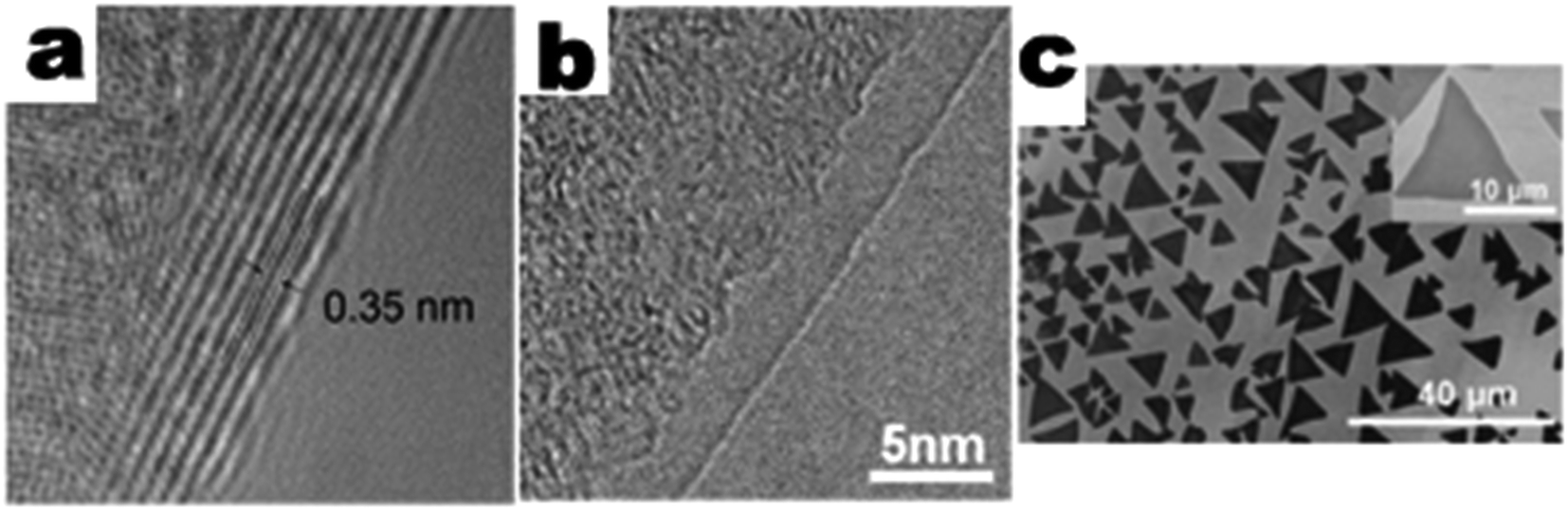
Growing single crystal BN nanosheets via CVD is still a big challenge and more efforts are obviously required. In one work, Gao et al. achieved individual single/double layer BN domains by altering the deposition time and concentration of the precursor (vaporized borazane) (Fig. 4b).68 The size of the individual BN domains was around 1 μm, and demonstrated the possibility of obtaining single crystal sheets by controlling the growth process. In another study, Wang et al. tried to regulate the nucleation process in the beginning of the CVD growth (Fig. 4c).70 The density of nucleation was significantly reduced by thoroughly annealing the Cu substrates under a reductive atmosphere (at 1050 °C for up to 6 hours) with ammonia borane as the precursor. BN single crystal sheets with sizes up to 20 μm were normally observed. Larger grains mean fewer domain boundaries and will lead to better performance in the future application of devices.
CVD growth of 2D transition metal dichalcogenides
TMDs are fundamentally and technologically intriguing due to their unique electronic and optical properties. The behaviors of TMDs are varied, ranging from insulating, semiconducting, truly metallic to superconducting. Reducing the stacking of TMDs to atomic layers leads to new characteristics induced by quantum confinement effects. Similar to graphene, single- and few-layer 2D TMD nanosheets can be obtained from either top-down routes like mechanical exfoliation or bottom-up processes like chemical vapor deposition (CVD). The aims of the CVD growth of TMDs are to grow few- and single- layer sheets, and to prepare single crystal TMD atomic layers. Atomic layer control offers controlled properties and single crystal atomic layers result in better performance over their polycrystalline counterparts in many device applications.CVD growth of TMDs dates back to 1988 when Hofmann demonstrated MOCVD growth of MoS2 and WS2 on various substrates.71 In this early work, MoS2 and WS2 were grown on various substrates, such as insulators/optical materials (glass, quartz, LiF, MgO and mica), transition metals and noble metals/conductors (Mo, Au, Pt, Al, Cu and steel). The precursors of Mo and W were hexacarbonyls of the corresponding transition metals and the precursor of S was vaporized sulfur or hydrogen sulfide gas. However, the films are normally thick. To prepare two dimensional atomic layers or single layers, several techniques in CVD have been developed. Liu et al. reported a two-step thermolysis process,72 in which ammonium thiomolybdates [(NH4)2MoS4] were dip-coated onto the substrates, and were converted to MoS2 by annealing at 500 °C under an Ar/H2 atmosphere followed by sulfurization at 1000 °C using sulfur vapor along with Ar gas. High-resolution TEM analysis identified that the thickness of MoS2 is three layers, and the MoS2 films could be easily transferred onto other arbitrary substrates. The sulfurization process with S vapor drastically enhanced the crystallinity of MoS2. In another work, few layer TMDs were obtained through conventional CVD processes. Zhan et al. reported the CVD growth of large-area MoS2 few-layer atomic layers based on the sulfurization of Mo metal films (Fig. 5a).73 A thin layer of Mo was deposited on SiO2 using an electronic beam evaporator before being placed in the tube furnace for CVD growth. Sulfur vapor was introduced into the process by heating the sulfur powder. The size of the grown MoS2 depended on the size of the substrates, and the thickness of the MoS2 depended on the thickness of the Mo films deposited on the substrates.
 | ||
| Fig. 5 (a) TEM image of CVD grown few layer MoS2, reprinted from ref. 73 by permission of John Wiley & Sons; (b) optical microscopy image of CVD synthesized single layer MoS2, reprinted from ref. 75 by permission of American Chemical Society; (c) SEM image of a CVD synthesized single crystal WS2 nanosheet, reprinted from ref. 82 by permission of the Royal Society of Chemistry. | ||
Besides elemental precursors, transition metal oxides could also be applied as the precursors. For example, Lee et al. synthesized few-layer MoS2 using CVD.74 In this work, MoO3 was converted to MoS2 by sulfurization. The pre-deposition treatments of substrates like SiO2 with aromatic molecules were applied to assist the growth of MoS2 atomic layers. However, in this work, full coverage of the substrates remained challenging. Liu et al. demonstrated a more delicate version of this technique,75 where a three-zone tube furnace with a much longer reaction zone and a stable temperature were required and the distance between sulfur and MoO3 could be adjusted without compromising the temperature zone (Fig. 5b). The as-synthesized MoS2 exhibited strong capabilities in gas and chemical sensing applications. Najmaei et al. modified this route further by hydrothermally synthesizing MoO3 nanoribbons to act as precursors of Mo.76 By altering the number of MoO3 nanoribbons dispersed onto the substrates, control over the Mo precursors and the resulting atomic layers was realized. McCreary et al. grew monolayer MoS2 films on graphene substrates.77 In this study, the precursor for Mo was MoCl5 which was different from most other works, and MoS2 films with 1, 2 or 3 layers were obtained by altering the amount of MoCl5. Huang et al. prepared large area monolayer WSe2 on sapphire substrates using CVD with WO3 and Se applied as the corresponding precursors.38 The CVD process was carried out under a mixed gas flow of Ar and H2, which assisted the activation of the reactions between Se and WO3. At a relatively low temperature of 750 °C, a continuous monolayer film of WSe2 was obtained.
CVD growth of single crystal TMDs is still a big challenge to date, and the obtained single crystal TMD flakes or domains achieved so far are relatively small compared to the single crystal graphene flakes. However, some success in the CVD growth of single crystal TMDs with large domain sizes has been realized recently. To grow single crystal TMDs, the main solutions are still to reduce the nucleation density to form larger domains/grains, and to control the growth process to obtain individual domains that form fewer or no domain boundaries. Laskar et al. demonstrated the CVD growth of large area single crystal MoS2 with (0001) orientation,78 where single crystal Al2O3 was applied as the substrate. The overall CVD process was basically the sulfurization of evaporated Mo thin films using sulfur vapor. By tuning the sulfurization time, high quality MoS2 films were obtained and were confirmed by planar view selective area diffraction patterns. However, the resulting films were relatively thick hindering further applications.
Besides elemental Mo and S, MoO3 and S could also be applied as precursors for the CVD growth of single crystal MoS2. Wang et al. demonstrated layer-by-layer sulfurization CVD growth of single crystal MoS2 flakes.79 The process was based on the conversion of MoO3 to MoS2 by sulfurization with vaporized S. Some MnO2 was introduced into the process to react with the excess sulfur. It should also be noted that the substrates were placed downstream of MoO3 rather than on top of it as in most cases. By controlling the deposition parameters, the layers of the obtained highly oriented MoS2 flakes could be controllably tuned from single, double, triple to quadruple layers. van der Zande et al. prepared monolayer single crystal MoS2 nanosheets with sizes up to 120 μm via CVD growth.80 The process was carried out under atmospheric pressure in a N2 gas flow, and a high yield was obtained with ultra clean substrates and fresh precursors.
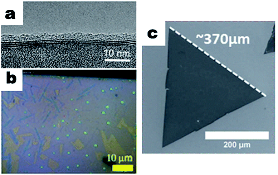
This process could be applied to other TMDs as well. Zhang et al. demonstrated the CVD growth of monolayer single crystal WS2 nanosheets on single crystal sapphire substrates using WO3 and S as precursors.81 The synthesis process was carried out under a low pressure at a temperature of ∼900 °C for ∼60 minutes and the products were monolayer single crystal WS2 nanosheets with sizes up to 50 μm. Rong et al. demonstrated the CVD growth of large single crystal domains of WS2 (Fig. 5c).82 By controlling the time and amount of sulfur introduced before and during the CVD process, monolayer WS2 domains with sizes up to 370 μm were obtained, which were visible to naked eye. The pre-deposition treatment of WO3 with sulfur was realized by heating the sulfur 15 minutes before the WO3 was heated up to the designated temperature for the CVD process. It should also be noted that, by loading aromatic molecules onto the substrates as seeding promoters, the synthesis of large monolayer single crystal TMDs is favored. For example, Ling et al. demonstrated the favored growth of large single crystal TMD monolayers with a substrate loaded with seeding promoters.83
Besides the TMD materials mentioned above, heterostructures based on TMD materials are attracting great interest. First principle calculations of band offsets predicted that certain kinds of TMD monolayer based heterostructures with type-II band alignment would be suitable for applications in the fields of photovoltaics, optoelectronics and energy conversion and storage.84 Other than type-II band alignments, heterostructures based on single-layer TMDs and graphene with Schottky barriers were also investigated by theoretical calculations. Bernardi et al. have theoretically demonstrated that bilayer solar cells of MoS2/graphene of 1 nm thickness could achieve over 1% power conversion efficiency.85 These theoretical works predicted that bilayers of TMD/TMD or TMD/graphene could be promising in various fields of applications. There are several experimental works on TMD based heterostructures. Huang et al. demonstrated lateral heterostructures within single layer MoSe2–WSe2 materials.86 The synthesis process was the vaporization and deposition of a mixture of MoSe2 and WSe2 with high purity H2 working as a carrier gas (Fig. 6). Duan et al. developed a CVD system that allowed the in situ switch of solid sources.87 By sequentially vaporizing and depositing WS2 and WSe2, WS2–WSe2 lateral heterostructures were obtained under high temperature, atmospheric pressure and vigorous Ar flow. Furthermore, Duan et al. also demonstrated the synthesis of single to few layer MoS2–MoSe2 lateral heterostructures using the same system. MoO3 was applied as precursor of Mo, when S and Se powders were sequentially vaporized and reacted with MoO3 to obtain MoS2–MoSe2 lateral heterostructures. Similarly, Zhang et al. demonstrated the CVD synthesis of TMD lateral heterostructures by the sequential CVD synthesis of the corresponding TMDs.88
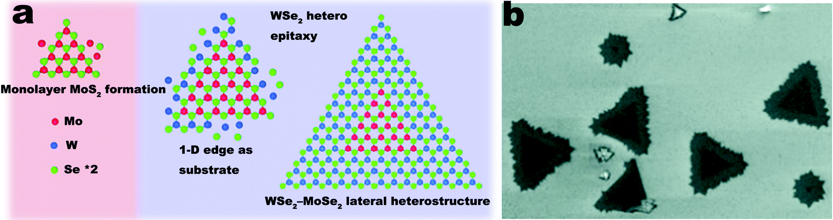 | ||
| Fig. 6 (a) Schematic illustration of the CVD growth process of WSe2–MoSe2 lateral heterostructures; (b) SEM image of WSe2–MoSe2 lateral heterostructures. Reprinted from ref. 86 by permission of American Chemical Society. | ||
Conclusion and perspective
We have briefly reviewed the CVD growth of two-dimensional materials, focusing on three types of signature 2D materials, graphene, BN and TMDs. The preparation processes and fundamental growth mechanisms of CVD growth, from few and single layer films to single crystal atomic sheets, are discussed. Substantial progress has been made in understanding the influence of the growth parameters, including precursors, substrates, atmospheres and gas flows.The development in the CVD growth of 2D materials is driven by the growing demand for high quality 2D materials in various fields of applications where full control of CVD growth is critical. However, such full control over the CVD growth process is still yet to be achieved. Complete understanding of the impact of the growth parameters has a special importance for realizing the programmable control of CVD growth and the high quality of grown 2D materials. For example, the synthesis of larger single crystal 2D materials with a quality comparable to those produced by mechanical exfoliation is still a big challenge. As for the CVD process, the key factors for larger single crystal 2D materials are the suppression of nucleation and well-maintained growth. Suppression of nucleation could be realized by thoroughly cleaning and smoothing the substrates, lowering the concentration of the precursors, and carrying out the process at a higher temperature. Well-maintained growth processes could be achieved by an optimized temperature, pressure and gas flow where slow growth may need a longer growth time than usual growth. In addition to the larger single crystal 2D materials, controllable CVD growth of heterostructures based on 2D materials and integration of the CVD growth of 2D materials with device fabrication are highly expected in the near future.
Acknowledgements
This work is supported by the National Basic Research Program of China (No. 2015CB258400), Natural Science Foundation of China (No. 51402118) and HUST.References
- A. de Lodyguine, US Patents, 1897, US575002A.
- R. Platz and S. Wagner, Appl. Phys. Lett., 1998, 73, 1236–1238 CrossRef CAS.
- K. L. Choy, Prog. Mater. Sci., 2003, 48, 57–170 CrossRef CAS.
- K. S. Novoselov, A. K. Geim, S. V. Morozov, D. Jiang, Y. Zhang, S. V. Dubonos, I. V. Grigorieva and A. A. Firsov, Science, 2004, 306, 666–669 CrossRef CAS PubMed.
- E. S. Penev, V. I. Artyukhov, F. Ding and B. I. Yakobson, Adv. Mater., 2012, 24, 4956–4976 CrossRef CAS PubMed.
- X. Zhang, H. Li and F. Ding, Adv. Mater., 2014, 26, 5488–5495 CrossRef CAS PubMed.
- I. Vlassiouk, M. Regmi, P. Fulvio, S. Dai, P. Datskos, G. Eres and S. Smirnov, ACS Nano, 2011, 5, 6069–6076 CrossRef CAS PubMed.
- P. R. Somani, S. P. Somani and M. Umeno, Chem. Phys. Lett., 2006, 430, 56–59 CrossRef CAS.
- W. Feng, S. Lei, Q. Li and A. Zhao, J. Phys. Chem. C, 2011, 115, 24858–24864 CrossRef CAS.
- T. Gao, S. Xie, Y. Gao, M. Liu, Y. Chen, Y. Zhang and Z. Liu, ACS Nano, 2011, 5, 9194–9201 CrossRef CAS PubMed.
- C.-M. Seah, S.-P. Chai and A. R. Mohamed, Carbon, 2014, 70, 1–21 CrossRef CAS.
- X. Li, W. Cai, L. Colombo and R. S. Ruoff, Nano Lett., 2009, 9, 4268–4272 CrossRef CAS PubMed.
- M. Eizenberg and J. Blakely, Surf. Sci., 1979, 82, 228–236 CrossRef CAS.
- J. Shelton, H. Patil and J. Blakely, Surf. Sci., 1974, 43, 493–520 CrossRef CAS.
- J. W. May, Surf. Sci., 1969, 17, 267–270 CrossRef CAS.
- A. Reina, X. Jia, J. Ho, D. Nezich, H. Son, V. Bulovic, M. S. Dresselhaus and J. Kong, Nano Lett., 2009, 9, 30–35 CrossRef CAS PubMed.
- A. J. Pollard, R. R. Nair, S. N. Sabki, C. R. Staddon, L. M. A. Perdigao, C. H. Hsu, J. M. Garfitt, S. Gangopadhyay, H. F. Gleeson, A. K. Geim and P. H. Beton, J. Phys. Chem. C, 2009, 113, 16565–16567 CrossRef CAS.
- X. S. Li, W. W. Cai, J. H. An, S. Kim, J. Nah, D. X. Yang, R. Piner, A. Velamakanni, I. Jung, E. Tutuc, S. K. Banerjee, L. Colombo and R. S. Ruoff, Science, 2009, 324, 1312–1314 CrossRef CAS PubMed.
- W. Fang, A. Hsu, Y. C. Shin, A. Liao, S. Huang, Y. Song, X. Ling, M. S. Dresselhaus, T. Palacios and J. Kong, Nanoscale, 2015, 7, 4929–4934 RSC.
- A. Ramasubramaniam, D. Naveh and E. Towe, Nano Lett., 2011, 11, 1070–1075 CrossRef CAS PubMed.
- S. Lee, K. Lee and Z. Zhong, Nano Lett., 2010, 10, 4702–4707 CrossRef CAS PubMed.
- K. Yan, H. Peng, Y. Zhou, H. Li and Z. Liu, Nano Lett., 2011, 11, 1106–1110 CrossRef CAS PubMed.
- Y. Gong, X. Zhang, G. Liu, L. Wu, X. Geng, M. Long, X. Cao, Y. Guo, W. Li, J. Xu, M. Sun, L. Lu and L. Liu, Adv. Funct. Mater., 2012, 22, 3153–3159 CrossRef CAS.
- Z. Tu, Z. Liu, Y. Li, F. Yang, L. Zhang, Z. Zhao, C. Xu, S. Wu, H. Liu, H. Yang and P. Richard, Carbon, 2014, 73, 252–258 CrossRef CAS.
- N. G. Shang, P. Papakonstantinou, M. McMullan, M. Chu, A. Stamboulis, A. Potenza, S. S. Dhesi and H. Marchetto, Adv. Funct. Mater., 2008, 18, 3506–3514 CrossRef CAS.
- J. Hwang, M. Kim, D. Campbell, H. A. Alsalman, J. Y. Kwak, S. Shivaraman, A. R. Woll, A. K. Singh, R. G. Hennig, S. Gorantla, M. H. Rümmeli and M. G. Spencer, ACS Nano, 2012, 7, 385–395 CrossRef PubMed.
- M. Wang, S. K. Jang, W.-J. Jang, M. Kim, S.-Y. Park, S.-W. Kim, S.-J. Kahng, J.-Y. Choi, R. S. Ruoff, Y. J. Song and S. Lee, Adv. Mater., 2013, 25, 2746–2752 CrossRef CAS PubMed.
- J. Chen, Y. Guo, L. Jiang, Z. Xu, L. Huang, Y. Xue, D. Geng, B. Wu, W. Hu, G. Yu and Y. Liu, Adv. Mater., 2014, 26, 1348–1353 CrossRef CAS PubMed.
- L. Gao, W. Ren, H. Xu, L. Jin, Z. Wang, T. Ma, L.-P. Ma, Z. Zhang, Q. Fu, L.-M. Peng, X. Bao and H.-M. Cheng, Nat. Commun., 2012, 3, 699 CrossRef PubMed.
- W. Wu, L. A. Jauregui, Z. Su, Z. Liu, J. Bao, Y. P. Chen and Q. Yu, Adv. Mater., 2011, 23, 4898–4903 CrossRef CAS PubMed.
- A. W. Robertson and J. H. Warner, Nano Lett., 2011, 11, 1182–1189 CrossRef CAS PubMed.
- X. Li, C. W. Magnuson, A. Venugopal, R. M. Tromp, J. B. Hannon, E. M. Vogel, L. Colombo and R. S. Ruoff, J. Am. Chem. Soc., 2011, 133, 2816–2819 CrossRef CAS PubMed.
- H. Wang, G. Wang, P. Bao, S. Yang, W. Zhu, X. Xie and W.-J. Zhang, J. Am. Chem. Soc., 2012, 134, 3627–3630 CrossRef CAS PubMed.
- S. Chen, H. Ji, H. Chou, Q. Li, H. Li, J. W. Suk, R. Piner, L. Liao, W. Cai and R. S. Ruoff, Adv. Mater., 2013, 25, 2062–2065 CrossRef CAS PubMed.
- Z. Yan, J. Lin, Z. Peng, Z. Sun, Y. Zhu, L. Li, C. Xiang, E. L. Samuel, C. Kittrell and J. M. Tour, ACS Nano, 2012, 6, 9110–9117 CrossRef CAS PubMed.
- L. Gan and Z. Luo, ACS Nano, 2013, 7, 9480–9488 CrossRef CAS PubMed.
- H. Zhou, W. J. Yu, L. Liu, R. Cheng, Y. Chen, X. Huang, Y. Liu, Y. Wang, Y. Huang and X. Duan, Nat. Commun., 2013, 4, 2096–2103 Search PubMed.
- J.-H. Lee, E. K. Lee, W.-J. Joo, Y. Jang, B.-S. Kim, J. Y. Lim, S.-H. Choi, S. J. Ahn, J. R. Ahn, M.-H. Park, C.-W. Yang, B. L. Choi, S.-W. Hwang and D. Whang, Science, 2014, 344, 286–289 CrossRef CAS PubMed.
- T. Wu, G. Ding, H. Shen, H. Wang, L. Sun, D. Jiang, X. Xie and M. Jiang, Adv. Funct. Mater., 2013, 23, 198–203 CrossRef CAS.
- Y. Xue, B. Wu, L. Jiang, Y. Guo, L. Huang, J. Chen, J. Tan, D. Geng, B. Luo, W. Hu, G. Yu and Y. Liu, J. Am. Chem. Soc., 2012, 134, 11060–11063 CrossRef CAS PubMed.
- Y. A. Wu, Y. Fan, S. Speller, G. L. Creeth, J. T. Sadowski, K. He, A. W. Robertson, C. S. Allen and J. H. Warner, ACS Nano, 2012, 6, 5010–5017 CrossRef CAS PubMed.
- D. Geng, B. Wu, Y. Guo, L. Huang, Y. Xue, J. Chen, G. Yu, L. Jiang, W. Hu and Y. Liu, Proc. Natl. Acad. Sci. U. S. A., 2012, 109, 7992–7996 CrossRef CAS PubMed.
- D. Geng, L. Meng, B. Chen, E. Gao, W. Yan, H. Yan, B. Luo, J. Xu, H. Wang, Z. Mao, Z. Xu, L. He, Z. Zhang, L. Peng and G. Yu, Adv. Mater., 2014, 26, 6423–6429 CrossRef CAS PubMed.
- A. Mohsin, L. Liu, P. Liu, W. Deng, I. N. Ivanov, G. Li, O. E. Dyck, G. Duscher, J. R. Dunlap, K. Xiao and G. Gu, ACS Nano, 2013, 7, 8924–8931 CrossRef CAS PubMed.
- Z. Yan, Y. Liu, L. Ju, Z. Peng, J. Lin, G. Wang, H. Zhou, C. Xiang, E. L. G. Samuel, C. Kittrell, V. I. Artyukhov, F. Wang, B. I. Yakobson and J. M. Tour, Angew. Chem., Int. Ed., 2014, 53, 1565–1569 CrossRef CAS PubMed.
- H. Mehdipour and K. Ostrikov, ACS Nano, 2012, 6, 10276–10286 CrossRef CAS PubMed.
- Y. Hao, M. S. Bharathi, L. Wang, Y. Liu, H. Chen, S. Nie, X. Wang, H. Chou, C. Tan, B. Fallahazad, H. Ramanarayan, C. W. Magnuson, E. Tutuc, B. I. Yakobson, K. F. McCarty, Y.-W. Zhang, P. Kim, J. Hone, L. Colombo and R. S. Ruoff, Science, 2013, 342, 720–723 CrossRef CAS PubMed.
- C. W. Magnuson, X. Kong, H. Ji, C. Tan, H. Li, R. Piner, C. A. Ventrice, Jr. and R. S. Ruoff, J. Mater. Res., 2014, 29, 403–409 CrossRef CAS.
- Z.-J. Wang, G. Weinberg, Q. Zhang, T. Lunkenbein, A. Klein-Hoffmann, M. Kurnatowska, M. Plodinec, Q. Li, L. Chi, R. Schloegl and M.-G. Willinger, ACS Nano, 2015, 9, 1506–1519 CrossRef CAS PubMed.
- H. O. Pierson, J. Compos. Mater., 1975, 9, 228–240 CrossRef CAS.
- E. Yamaguchi and M. Minakata, J. Appl. Phys., 1984, 55, 3098–3102 CrossRef CAS.
- K. Nakamura, J. Electrochem. Soc., 1985, 132, 1757–1762 CrossRef CAS.
- K. Nakamura, J. Electrochem. Soc., 1986, 133, 1120–1123 CrossRef CAS.
- H. Saitoh and W. A. Yarbrough, Appl. Phys. Lett., 1991, 58, 2482–2484 CrossRef CAS.
- L. Maya and H. L. Richards, J. Am. Ceram. Soc., 1991, 74, 406–409 CrossRef CAS.
- Y. Shi, C. Hamsen, X. Jia, K. K. Kim, A. Reina, M. Hofmann, A. L. Hsu, K. Zhang, H. Li, Z.-Y. Juang, M. S. Dresselhaus, L.-J. Li and J. Kong, Nano Lett., 2010, 10, 4134–4139 CrossRef CAS PubMed.
- L. Song, L. Ci, H. Lu, P. B. Sorokin, C. Jin, J. Ni, A. G. Kvashnin, D. G. Kvashnin, J. Lou, B. I. Yakobson and P. M. Ajayan, Nano Lett., 2010, 10, 3209–3215 CrossRef CAS PubMed.
- M. Corso, W. Auwärter, M. Muntwiler, A. Tamai, T. Greber and J. Osterwalder, Science, 2004, 303, 217–220 CrossRef CAS PubMed.
- W. Auwärter, H. U. Suter, H. Sachdev and T. Greber, Chem. Mater., 2003, 16, 343–345 CrossRef.
- R. J. Simonson, M. T. Paffett, M. E. Jones and B. E. Koel, Surf. Sci., 1991, 254, 29–44 CrossRef CAS.
- M. T. Paffett, R. J. Simonson, P. Papin and R. T. Paine, Surf. Sci., 1990, 232, 286–296 CrossRef CAS.
- A. Nagashima, N. Tejima, Y. Gamou, T. Kawai and C. Oshima, Phys. Rev. Lett., 1995, 75, 3918–3921 CrossRef CAS PubMed.
- A. Preobrajenski, A. Vinogradov, M. Ng, E. Ćavar, R. Westerström, A. Mikkelsen, E. Lundgren and N. Mårtensson, Phys. Rev. B: Condens. Matter Mater. Phys., 2007, 75, 245412 CrossRef.
- P. Sutter, J. Lahiri, P. Albrecht and E. Sutter, ACS Nano, 2011, 5, 7303–7309 CrossRef CAS PubMed.
- A. Ismach, H. Chou, D. A. Ferrer, Y. Wu, S. McDonnell, H. C. Floresca, A. Covacevich, C. Pope, R. Piner, M. J. Kim, R. M. Wallace, L. Colombo and R. S. Ruoff, ACS Nano, 2012, 6, 6378–6385 CrossRef CAS PubMed.
- G. Kim, A. R. Jang, H. Y. Jeong, Z. Lee, D. J. Kang and H. S. Shin, Nano Lett., 2013, 13, 1834–1839 CrossRef CAS PubMed.
- K. K. Kim, A. Hsu, X. Jia, S. M. Kim, Y. Shi, M. Hofmann, D. Nezich, J. F. Rodriguez-Nieva, M. Dresselhaus, T. Palacios and J. Kong, Nano Lett., 2011, 12, 161–166 CrossRef PubMed.
- Y. Gao, W. Ren, T. Ma, Z. Liu, Y. Zhang, W.-B. Liu, L.-P. Ma, X. Ma and H.-M. Cheng, ACS Nano, 2013, 7, 5199–5206 CrossRef CAS PubMed.
- J.-H. Park, J. C. Park, S. J. Yun, H. Kim, D. H. Luong, S. M. Kim, S. H. Choi, W. Yang, J. Kong, K. K. Kim and Y. H. Lee, ACS Nano, 2014, 8, 8520–8528 CrossRef CAS PubMed.
- L. Wang, B. Wu, J. Chen, H. Liu, P. Hu and Y. Liu, Adv. Mater., 2014, 26, 1559–1564 CrossRef CAS PubMed.
- W. Hofmann, J. Mater. Sci., 1988, 23, 3981–3986 CrossRef CAS.
- K.-K. Liu, W. Zhang, Y.-H. Lee, Y.-C. Lin, M.-T. Chang, C.-Y. Su, C.-S. Chang, H. Li, Y. Shi, H. Zhang, C.-S. Lai and L.-J. Li, Nano Lett., 2012, 12, 1538–1544 CrossRef CAS PubMed.
- Y. Zhan, Z. Liu, S. Najmaei, P. M. Ajayan and J. Lou, Small, 2012, 8, 966–971 CrossRef CAS PubMed.
- Y. H. Lee, X. Q. Zhang, W. Zhang, M. T. Chang, C. T. Lin, K. D. Chang, Y. C. Yu, J. T. Wang, C. S. Chang, L. J. Li and T. W. Lin, Adv. Mater., 2012, 24, 2320–2325 CrossRef CAS PubMed.
- B. Liu, L. Chen, G. Liu, A. N. Abbas, M. Fathi and C. Zhou, ACS Nano, 2014, 8, 5304–5314 CrossRef CAS PubMed.
- S. Najmaei, Z. Liu, W. Zhou, X. Zou, G. Shi, S. Lei, B. I. Yakobson, J.-C. Idrobo, P. M. Ajayan and J. Lou, Nat. Mater., 2013, 12, 754–759 CrossRef CAS PubMed.
- K. M. McCreary, A. T. Hanbicki, J. T. Robinson, E. Cobas, J. C. Culbertson, A. L. Friedman, G. G. Jernigan and B. T. Jonker, Adv. Funct. Mater., 2014, 24, 6449–6454 CrossRef CAS.
- M. R. Laskar, L. Ma, S. Kannappan, P. Sung Park, S. Krishnamoorthy, D. N. Nath, W. Lu, Y. Wu and S. Rajan, Appl. Phys. Lett., 2013, 102, 252108 CrossRef.
- X. Wang, H. Feng, Y. Wu and L. Jiao, J. Am. Chem. Soc., 2013, 135, 5304–5307 CrossRef CAS PubMed.
- A. M. van der Zande, P. Y. Huang, D. A. Chenet, T. C. Berkelbach, Y. You, G. H. Lee, T. F. Heinz, D. R. Reichman, D. A. Muller and J. C. Hone, Nat. Mater., 2013, 12, 554–561 CrossRef PubMed.
- Y. Zhang, Y. Zhang, Q. Ji, J. Ju, H. Yuan, J. Shi, T. Gao, D. Ma, M. Liu, Y. Chen, X. Song, H. Y. Hwang, Y. Cui and Z. Liu, ACS Nano, 2013, 7, 8963–8971 CrossRef CAS PubMed.
- Y. Rong, Y. Fan, A. Leen Koh, A. W. Robertson, K. He, S. Wang, H. Tan, R. Sinclair and J. H. Warner, Nanoscale, 2014, 6, 12096–12103 RSC.
- X. Ling, Y.-H. Lee, Y. Lin, W. Fang, L. Yu, M. S. Dresselhaus and J. Kong, Nano Lett., 2014, 14, 464–472 CrossRef CAS PubMed.
- J. Kang, S. Tongay, J. Zhou, J. Li and J. Wu, Appl. Phys. Lett., 2013, 102, 012111 CrossRef.
- M. Bernardi, M. Palummo and J. C. Grossman, Nano Lett., 2013, 13, 3664–3670 CrossRef CAS PubMed.
- C. Huang, S. Wu, A. M. Sanchez, J. J. P. Peters, R. Beanland, J. S. Ross, P. Rivera, W. Yao, D. H. Cobden and X. Xu, Nat. Mater., 2014, 13, 1096–1101 CrossRef CAS PubMed.
- X. Duan, C. Wang, J. C. Shaw, R. Cheng, Y. Chen, H. Li, X. Wu, Y. Tang, Q. Zhang, A. Pan, J. Jiang, R. Yu, Y. Huang and X. Duan, Nat. Nanotechnol., 2014, 9, 1024–1030 CrossRef CAS PubMed.
- X.-Q. Zhang, C.-H. Lin, Y.-W. Tseng, K.-H. Huang and Y.-H. Lee, Nano Lett., 2015, 15, 410–415 CrossRef CAS PubMed.
| This journal is © The Royal Society of Chemistry 2015 |