
Probing thermal expansion coefficients of monolayers using surface enhanced Raman scattering
Duan Zhang†
a,
Ye-Cun Wu†a,
Mei Yanga,
Xiao Liua,
Cormac Ó Coileáinabc,
Hongjun Xuab,
Mourad Abidb,
Mohamed Abidb,
Jing-Jing Wangc,
Igor V. Shvetsc,
Haonan Liua,
Zhi Wanga,
Hongxing Yina,
Huajun Liud,
Byong Sun Chune,
Xiangdong Zhanga and
Han-Chun Wu*a
aBeijing Key Lab of Nanophotonics and Ultrafine Optoelectronic Systems, School of Physics, Beijing Institute of Technology, Beijing 100081, P. R. China. E-mail: wuhc@bit.edu.cn
bKSU-Aramco Center, King Saud University, Riyadh 11451, Saudi Arabia
cCRANN, School of Physics, Trinity College, University of Dublin, Dublin 2, Ireland
dInstitute of Plasma Physics, Chinese Academy of Sciences, Hefei 230031, P. R. China
eDivision of Industrial Metrology, Korea Research Institute of Standards and Science, Daejeon 305-340, South Korea
First published on 13th October 2016
Abstract
Monolayer transition metal dichalcogenides exhibit remarkable electronic and optical properties, making them candidates for application within flexible nano-optoelectronics, however direct experimental determination of their thermal expansion coefficients (TECs) is difficult. Here, we propose a non-destructive method to probe the TECs of monolayer materials using surface-enhanced Raman spectroscopy (SERS). A strongly coupled Ag nanoparticle over-layer is used to controllably introduce temperature dependent strain in monolayers. Changes in the first-order temperature coefficient of the Raman shift, produced by TEC mismatch, can be used to estimate relative expansion coefficient of the monolayer. As a demonstration, the linear TEC of monolayer WS2 is probed and is found to be 10.3 × 10⁻⁶ K−1, which would appear support theoretical predictions of a small TEC. This method opens a route to probe and control the TECs of monolayer materials.
Two dimensional (2D) materials, such as transition metal dichalcogenides (TMDs), have attracted much attention due to their outstanding electronic and optical attributes.1–10 For integration with existing semiconductor technology 2D TMDs have a natural advantage over graphene, in that they typically possess an energy bandgap, and yet can display high carrier mobilities. The bandgaps of TMDs are thickness dependent, typically displaying a transition from an indirect to direct-bandgap when the thickness is reduced to a monolayer.2,3,11,12 However, a key physical consideration for the application of 2D materials is their thermal expansion coefficient (TEC), which relates changes in dimension to temperature. While many of the optical and electronic properties of TMDs have been well characterized, the thermal properties of many 2D materials remain less explored due to the difficulties associated with experimental measurements. Most materials exhibit positive thermal expansion, expanding when heated and contracting when cooled. However some materials do exhibit negative thermal expansion, and an interesting few exhibit very low (less than 2 × 10⁻⁶
![[thin space (1/6-em)]](https://www.rsc.org/images/entities/char_2009.gif) K−1) or zero thermal expansion within specific temperature ranges.13 A small TEC is highly desirable for applications where there is little tolerance for dimensional change or for systems that experience rapid temperature variations but require consistency, such as for nano-electro-mechanical devices14 or nanosensors.15 It is well known that the origin of thermal expansion is anharmonic atomic lattice interactions, where the average interatomic distances increase as higher vibrational energy levels become available and are occupied. Therefore, crystal structure can greatly affect the TEC, for example, diamond is a positive TEC material,16 graphite exhibits negative in-plane but positive out-of-plane TECs,17 and from experiment and theoretical predictions, graphene is recognized as having a negative TEC over a wide range of temperatures.18–23 Other 2D materials such as monolayer hexagonal boron nitride are also predicted to exhibit a negative TEC.21,22 On the other hand, 2D TMDs are generally believed to demonstrate positive TECs.23,24 Specifically, recent first principles calculations have indicated that the linear TEC of monolayer WS2 is very small.24 Bulk WS2 has an indirect bandgap of 1.3 eV, whereas a monolayer has direct bandgap of 2.1 eV,12 and another notable feature is intense photoluminescence (PL) found for monolayer WS2.25 These properties suggest that such monolayers have potential for applications within flexible 2D nano-optoelectronics. However, the claim of a small TEC is yet to be experimentally confirmed due to the difficulties associated with measuring expansion at the length scales associated with 2D materials. For monolayer materials the thermal expansion coefficient can be ideally experimentally determined through delicate nanoelectromechanical resonance measurements or direct imaging of rippling of suspended monolayers.26,27 However these methods require intricate device fabrication or extensive careful imaging.
K−1) or zero thermal expansion within specific temperature ranges.13 A small TEC is highly desirable for applications where there is little tolerance for dimensional change or for systems that experience rapid temperature variations but require consistency, such as for nano-electro-mechanical devices14 or nanosensors.15 It is well known that the origin of thermal expansion is anharmonic atomic lattice interactions, where the average interatomic distances increase as higher vibrational energy levels become available and are occupied. Therefore, crystal structure can greatly affect the TEC, for example, diamond is a positive TEC material,16 graphite exhibits negative in-plane but positive out-of-plane TECs,17 and from experiment and theoretical predictions, graphene is recognized as having a negative TEC over a wide range of temperatures.18–23 Other 2D materials such as monolayer hexagonal boron nitride are also predicted to exhibit a negative TEC.21,22 On the other hand, 2D TMDs are generally believed to demonstrate positive TECs.23,24 Specifically, recent first principles calculations have indicated that the linear TEC of monolayer WS2 is very small.24 Bulk WS2 has an indirect bandgap of 1.3 eV, whereas a monolayer has direct bandgap of 2.1 eV,12 and another notable feature is intense photoluminescence (PL) found for monolayer WS2.25 These properties suggest that such monolayers have potential for applications within flexible 2D nano-optoelectronics. However, the claim of a small TEC is yet to be experimentally confirmed due to the difficulties associated with measuring expansion at the length scales associated with 2D materials. For monolayer materials the thermal expansion coefficient can be ideally experimentally determined through delicate nanoelectromechanical resonance measurements or direct imaging of rippling of suspended monolayers.26,27 However these methods require intricate device fabrication or extensive careful imaging.
Here we propose a relatively simple non-destructive method to probe the TECs of monolayer materials using surface-enhanced Raman spectroscopy (SERS). A strongly coupled metallic nanoparticle (NP) over-layer is used to controllably introduce strain in the monolayers. The vibrational modes of the monolayer are sensitive to strain resulting from TEC mismatch, which are probed in temperature dependent Raman measurements. For monolayer WS2, the out-of-plane linear TEC is found to be at most ∼10.3 × 10⁻⁶ K−1, which would appear support theoretical predictions of a small TEC. We also use monolayer MoS2 to show how the magnitude of the strain corresponds to the degree of TEC mismatch. This experimental study suggests how the thermal properties of monolayer materials could be tuned and how the TECs of monolayer materials can be investigated in a nondestructive manner. The method proposed here is robust, and would be suitable for probing the TECs both for supported and freestanding monolayers.
Results and discussion
Fig. 1a shows a schematic of the proposed method. A strongly coupled metallic nanoparticle (NP) over-layer with a comparatively larger TEC is added to introduce strain in the TMD monolayer. Cooling induces contraction of metal NPs and strains the TMD monolayer. The magnitude of this strain is in proportion to the mismatch between the TECs. Thus the vibrational modes of the monolayer with NPs will be shifted with respect to the bare monolayer, which can be clearly observed during temperature dependent Raman measurements.28,29 Since the origin of thermal expansion is anharmonic atomic lattice interactions, a quasi-harmonic approximation can be used to express the change in the phonon frequency (ω) with temperature (T) in terms of the contribution made by thermal expansion in the lattice.30,31
 | (1) |
 can be determined from the Raman measurements, while the change with lattice constant
  has to be effectively determined through first-principles density functional theory calculations.30 In our proposed method we measure the change in the Raman frequency with temperature with (χML+NP) and without (χML) metal nanoparticles. Since the metallic nanoparticles are deposited by an e-beam evaporator and strongly coupled with the monolayer underneath, the thermal expansion for coupled system is mainly controlled by NPs. Thus with nanoparticles eqn (1) becomes
 | (2) |
 should not change for SERS measurements, we can calculate the expansion coefficient of monolayer from the relative change
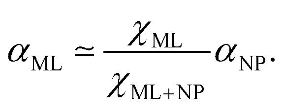 | (3) |
 | ||
| Fig. 1 SERS of monolayer WS2 at room temperature. (a) Schematic drawing of the experimental setup of the SERS measurements of WS2. (b) Raman spectra of monolayer WS2 with (Red) and without (Black) 5 nm nominally thick Ag NPs on top. Arrow indicates the splitting of the A′1(Γ) mode. (c) SEM image of 5 nm nominally thick Ag NPs on monolayer WS2. (d) Simulated electric field cartography at the surface of the area marked in Fig. 1c with an excitation wavelength of 532 nm. | ||
As the thermal expansion coefficient of the metal is known, it allows us to estimate the TECs of the bare monolayers using SERS. The advantages of our proposed method can be summarized as follows. First, the metallic NPs act as a reference point to determine the TEC of the monolayer. Second, SERS allows us to check for local strain within the monolayer to ensure strong coupling between the nanoparticles and monolayer, and gives a better signal to noise ratio. Third, metal has a high thermal conductivity; it can help prevent burning of the monolayer when laser is switched on. Fourth, the approach we propose could be used for wide variety of monolayers, even layers with mixed compositions, provided there is strong coupling with a nanoparticles over-layer. While it is known that SERS can suffer from issues of reproducibility, in our proposed method the nanoparticles are prepared by e-beam evaporation, thus provided the same growth conditions are maintained the distribution on the surface should be consistent. Furthermore, it is the intensity of the SERS signal that typically suffers from issues of reproducibility, which is not a factor within our calculations. The relative change in the peak position is the factor under consideration, and in fact similar consistent behaviour was observed for more than five different experiments.
To demonstrate the proposed method, the TEC of monolayer WS2 was probed using SERS, stimulated by a coating of Ag NPs on top, which was deposited by e-beam evaporation. The large-scale continuous WS2 monolayers were produced by sulfurization of monolayer oxide films, further details of sample preparation and characterization can be found in the methods section and elsewhere.32 Fig. 1b displays the room temperature Raman spectra for monolayer WS2 without and with Ag NPs. The Raman spectrum displays peaks for the in-plane active modes E′(Γ) and out-of-plane modes A′1(Γ) at around 356 cm−1 and 417 cm−1, respectively, and the second-order zone-edge phonon peak 2LA(M) at approximately 353 cm−1. Compared with bulk WS2,33 the out-of-plane mode A′1(Γ) is red-shifted from 421 to 417 cm−1, resulting from the absence of van der Waals interactions between the layers. As would be expected, the addition of the 5 nm thick Ag NP layer leads to a clear enhancement of Raman intensity, as shown in Fig. 1b. However, this enhancement is also accompanied by a slight red-shift of the E′(Γ) mode and additional peaks appear, caused by a strain of approximately 1% in the WS2 induced by the NPs.32,34 The modification of the Raman spectra by the Ag NP over-layer can be can be understood considering two contributing factors; strain and electric field enhancement. First considering strain, the application strain can frustrate the lattice symmetry, leading to peak splitting in the Raman spectra. The application of tensile strain will predominantly lead to changes in the in-plane vibrational modes, while mechanical or compressive strain, such as that exerted by the Ag NPs on top, will lead to greater modification of the out of plane modes. The addition of the Ag results in several sources of stress in the monolayers. The Ag nanoparticles grow in an island formation, as seen in Fig. 1c, were atom clusters nucleate on the monolayer surface and grow forming isolated islands as long as there is exposed surface, and since Ag is quite mobile even near room temperature, larger islands will grow at the expense of the shrinking of small islands.35 The thermodynamic processes, such as surface tension, that drive the formation of the NPs will introduce stress between the Ag and monolayer. The area directly under the NPs will be the most highly strained, with a gradient at the edges towards uncovered areas. However, interestingly, it has been experimentally observed that the degree mechanical strain is largely independent of the NP size.34 Notably strain from lattice mismatch is not expected to be a significant contributing factor to within Ag NP films grown by e-beam.36 However, during temperature dependent measurements strain can also be generated due to the mismatch in the TECs of the materials. For these experiments, the high thermal conductivity of Ag means that a thermal gradient is not expected, and since the bonding of WS2 to the Al2O3 substrate is quite weak it is expected that strain from the Ag NPs will be the dominant factor.37
Considering the electric field enhancement, in the vicinity of the Ag NPs the electric field will be enhanced due to the collective oscillations of the conduction electrons. Thus the scattering process is enhanced by a factor of (Elocal/E0)4, where E0 is the strength of the incident E-field and Elocal is the strength of the total local electric field in the presence of the metallic NPs.34,38,39 For example, the intensity of the 2LA(M) mode is enhanced by a factor of 3. Using finite-difference time-domain (FDTD) methods, we simulated the electrical field distribution of an area of monolayer WS2 containing several 5 nm nominal thickness Ag NPs (Fig. 1d). It is clear from the figure that the strength of the localized electric field depends on the size, shape and interactions between the individual NPs. The lightning rod effect is an important factor in determining the strength of the electric field, which causes the field to be dramatically enhanced around sharp edges.
To assess the influence temperature has on the expansion of WS2 we focus on two Raman peaks, the in-plane E′(Γ) and the out-of-plane A′1(Γ) modes. The Raman spectra of both the E′(Γ) and A′1(Γ) modes blue shift to higher wave-numbers when the temperature is decreased from 300 K and 120 K, as seen in respectively in Fig. 2a and b for WS2 with Ag NPs. This trend can be further illustrated by plotting the peak position of the Raman shifts against temperature as shown in Fig. 2c and d. It is worth noting that the 2LA(M) mode (Fig. 2c) also follows a similar dependence and that similar blue shifts were observed for WS2 without Ag (Fig. 3a). The shift of the Raman peaks with temperature is mainly due to thermal expansion and the temperature contribution from anharmonicity. To quantify this behavior, the temperature dependent Raman shift for the E′(Γ) and A′1(Γ) modes can be fitted using the Grüneisen model:40
ω(T) = ω0 + χ![[thin space (1/6-em)]](https://www.rsc.org/images/entities/i_char_2009.gif) T T
| (4) |
 | ||
| Fig. 2 Temperature dependent Raman shifts of monolayer WS2 with 5 nm nominally thick Ag NPs on top. Raman spectra for (a) E′(Γ) mode, and (b) A′1(Γ) mode recorded at various temperatures from 120 K to 300 K. Variation of Raman frequencies as a function of temperature for (c) E′(Γ), 2LA(M) and (d) A′1(Γ) modes. | ||
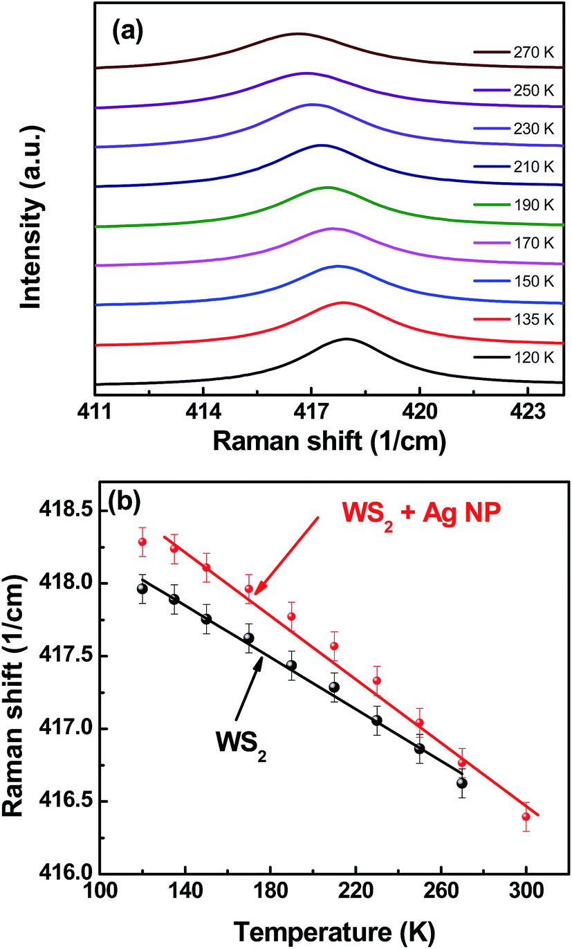 | ||
| Fig. 3 Temperature dependent Raman shifts of bare monolayer WS2. (a) Raman spectra of A′1(Γ) mode recorded for various temperatures ranging from 110 K to 300 K. (b) Variation of Raman frequencies as a function of temperature for the A′1(Γ) mode for WS2 and WS2 + Ag NP. | ||
Considering the quasi-harmonic approximation discussed previously,30,31 from eqn (1) we know χ ∝ α. It should be noted that as the WS2 layer is only weakly bound to the Al2O3, the monolayer should be initially relaxed and not strained by the substrate for both samples.35 The volumetric thermal expansion coefficients of bulk Ag and the WS2 are relatively well matched24,44,45 (see Table 1), however the change in χ for the E′(Γ) and A′1(Γ) modes, with the addition of Ag NPs, suggests compressive strain with decreasing temperature. This would occur if the TEC of Ag was greater than that of the WS2 monolayer, as the Ag would contract at a faster rate, suggesting that the TEC of monolayer WS2 is significantly less than that of the bulk. For the A′1(Γ) mode the blue shift of 0.3 cm−1 corresponds to compressive strain of approximately 3%.46 From the χ values of the A′1(Γ) mode with (χAg) and without (χWS2) Ag, using eqn (3) we can calculate that the out-of-plane α for monolayer WS2 is at most 55% the TEC of Ag, which corresponds to a TEC of 10.3 × 10⁻⁶ K−1. Our experimental results appear to support recent first principles calculations.24
To demonstrate the versatility of this approach, an analogous experiment was also performed with monolayer MoS2, where the thermal expansion coefficient of MoS2 (αMoS2) is slightly larger than that of Ag (αAg) (Table 1). Fig. 4a shows the temperature dependent Raman spectra for a monolayer of MoS2 with 5 nm of Ag NPs grown on top. Fig. 4b and c plot peak position of the temperature dependent Raman shifts for the E′(Γ) and A′1(Γ) modes with Ag NPs. As αMoS2 > αAg, dramatic modification of χ is not expected. From Fig. 4b and c, the χ values for the E′(Γ) and A′1(Γ) modes are ∼−0.012 and ∼−0.018 cm−1 K−1 with Ag, which are consistent with reports for MoS2 with Ag.47–50 The lack of a significant change in χ with the addition of the NPs suggests the MoS2 is less strained at low temperature and thus TECs of Ag and MoS2 are broadly similar.
 | ||
| Fig. 4 Temperature dependent Raman shifts of monolayer MoS2 with 5 nm nominally thick Ag NPs on top. (a) Raman spectra recorded at various temperatures from 120 K to 300 K. (b) and (c) are variation of Raman frequencies as a function of temperature for E′(Γ) and A′1(Γ) modes respectively. | ||
Conclusion
We used temperature dependent SERS to probe the TECs of monolayer TMDs. Temperature dependent strain in the monolayer is induced by the TEC mismatch between the monolayer and the strongly coupled Ag NP over-layer. This allows used to access the linear TECs of the monolayers from changes in the first order linear thermal coefficients of in-plane and out of plane modes. Using this approach we demonstrated the small TEC of monolayer WS2. This method could be expanded and refined for a broad range of NP and monolayer materials, and also suggests how expansion of monolayers could be controlled.Methods
The monolayer WO3 was deposited on single crystal α-Al2O3 (0001) substrates at 400 °C using an e-beam heated WO3 source in a MBE system (DCA) with in an oxygen partial pressure of 5 × 10⁻⁶ Torr. Reflection high electron diffraction (RHEED) was employed to monitor and establish growth mode. After growth, the WO3 monolayers were annealed at 650 °C, with the same pressure for 30 minutes. The oxide samples were removed from vacuum and sulfurized in a furnace using 10% H2 in argon gas as the carrier. MoS2 was grown using a similar procedure. The Ag nanoparticles with a 5 nm nominal thickness were deposited on the monolayers at room temperature by e-beam evaporation. The high quality and chemical composition of the samples was verified before and after sulfurization by X-ray photoemission spectroscopy (XPS). Raman spectroscopy, and PL spectroscopy were used to further evaluate the thickness of the WS2 layer. Raman measurements were performed using a Renishaw RM1000 spectrometer with an excitation wavelength of 532 nm. The temperature of sample was controlled by a Linkam LTHMS600E microscopy stage which has a temperature range of −196 °C to 600 °C. During the measurement, we used 50× Leica long-focus objective lens and the power of laser was set to be 1%. A bandgap of ∼2 eV is observed indicating the grown WS2 is monolayer in nature.25Author contributions
H. C. W. supervised the project and led the overall effort. D. Z., Y. C. W., M. Y. and X. L. carried out the Raman measurements. C. O., MOH. A., and I. V. S. grew the sample. MOU. A. performed the FDTD simulation. H. L. and Z. W. deposited the Ag nanoparticles. H. X. Y. carried out the SEM characterization. D. Z., Y. C. W., J. J. W., H. J. X., and H. C. W. analyzed the data. H. J. L. and B. S. C. commented the paper. X. D. Z. gave scientific advice. H. C. W. wrote the paper. All authors discussed the results and commented on the manuscript.Competing financial interests
The authors declare there is no competing financial interest.Acknowledgements
This work was supported by the Beijing Institute of Technology Research Fund Program for Young Scholars and National Plan for Science and technology (No. NPST 2472-02 and NPST 2529-02) of King Abdulaziz City for Science and Technology. H. C. W., MOH. A., and MOU. A. thank Saudi Aramco for the financial support (project No. 6600028398).References
- K. Novoselov, D. Jiang, F. Schedin, T. Booth, V. Khotkevich, S. Morozov and A. Geim, Proc. Natl. Acad. Sci. U. S. A., 2005, 102, 10451 CrossRef CAS PubMed.
- Q. Wang, K. Kalantar-Zadeh, A. Kis, J. Coleman and M. Strano, Nat. Nanotechnol., 2012, 7, 699–712 CrossRef CAS PubMed.
- K. Mak, C. Lee, J. Hone, J. Shan and T. Heinz, Phys. Rev. Lett., 2010, 105, 136805 CrossRef PubMed.
- G. Eda and S. Maier, ACS Nano, 2013, 7, 5660 CrossRef CAS PubMed.
- B. Radisavljevic, A. Radenovic, J. Brivio, V. Giacometti and A. Kis, Nat. Nanotechnol., 2011, 6, 147 CrossRef CAS PubMed.
- D. Xiao, G. Liu, W. Feng, X. Xu and W. Yao, Phys. Rev. Lett., 2012, 108, 196802 CrossRef PubMed.
- K. Mak, K. McGill, J. Park and P. McEuen, Science, 2014, 344, 1489 CrossRef CAS PubMed.
- R. Mas-Ballesté, C. Gómez-Navarro, J. Gómez-Herrero and F. Zamora, Nanoscale, 2011, 3, 20 RSC.
- A. Rodin, A. Carvalho and A. Castro Neto, Phys. Rev. Lett., 2014, 112, 176801 CrossRef CAS PubMed.
- W. Zhang, Q. Wang, Y. Chen, Z. Wang and A. Wee, 2D Mater., 2016, 3, 022001 CrossRef.
- W. Zhao, Z. Ghorannevis, L. Chu, M. Toh, C. Kloc, P. Tan and G. Eda, ACS Nano, 2013, 7, 791 CrossRef CAS PubMed.
- A. Kuc, N. Zibouche and T. Heine, Phys. Rev. B: Condens. Matter Mater. Phys., 2011, 83, 245213 CrossRef.
- R. Roy, D. Agrawal and H. McKinstry, Annu. Rev. Mater. Sci., 1989, 19, 59 CrossRef CAS.
- S. Jun, X. Huang, M. Manolidis, C. Zorman, M. Mehregany and J. Hone, Nanotechnology, 2006, 17, 1506 CrossRef CAS.
- Y. Gao and Y. Bando, Nature, 2002, 415, 599 CrossRef CAS PubMed.
- R. Krishnan, Nature, 1944, 154, 486 CrossRef CAS.
- D. Tsang, B. Marsden, S. Fok and G. Hall, Carbon, 2005, 43, 2902 CrossRef CAS.
- V. Singh, S. Sengupta, H. Solanki, R. Dhall, A. Allain, S. Dhara, P. Pant and M. Deshmukh, Nanotechnology, 2010, 21, 165204 CrossRef PubMed.
- D. Yoon, Y. Son and H. Cheong, Nano Lett., 2011, 11, 3227 CrossRef CAS PubMed.
- A. Balandin, Nat. Mater., 2011, 10, 569 CrossRef CAS PubMed.
- K. Zakharchenko, J. Los, M. Katsnelson and A. Fasolino, Phys. Rev. B: Condens. Matter Mater. Phys., 2010, 81, 235439 CrossRef.
- L. Feng Huang and Z. Zeng, J. Appl. Phys., 2013, 113, 083524 CrossRef.
- C. Sevik, Phys. Rev. B: Condens. Matter Mater. Phys., 2014, 89, 035422 CrossRef.
- Y. Ding and B. Xiao, RSC Adv., 2015, 5, 18391 RSC.
- N. Peimyoo, J. Shang, C. Cong, X. Shen, X. Wu, E. Yeow and T. Yu, ACS Nano, 2013, 7, 10985 CrossRef CAS PubMed.
- W. Bao, F. Miao, Z. Chen, H. Zhang, W. Jang, C. Dames and C. Lau, Nat. Nanotechnol., 2009, 4, 562 CrossRef CAS PubMed.
- V. Singh, S. Sengupta, H. Solanki, R. Dhall, A. Allain, S. Dhara, P. Pant and M. Deshmukh, Nanotechnology, 2010, 21, 165204 CrossRef PubMed.
- C. Cong and T. Yu, Nat. Commun., 2014, 5, 4709 CAS.
- I. Calizo, A. Balandin, W. Bao, F. Miao and C. Lau, Nano Lett., 2007, 7, 2645 CrossRef CAS PubMed.
- D. Late, S. Shirodkar, U. Waghmare, V. Dravid and C. Rao, ChemPhysChem, 2014, 15, 1592 CrossRef CAS PubMed.
- M. Upadhyay Kahaly and U. Waghmare, Appl. Phys. Lett., 2007, 91, 023112 CrossRef.
- D. Zhang, Y. Wu, M. Yang, X. Liu, C. Coileáin, M. Abid, M. Abid, J. Wang, I. Shvets, H. Xu, B. Chun, H. Liu and H. Wu, Sci. Rep., 2016, 6, 30320 CrossRef CAS PubMed.
- X. Zhang, X. Qiao, W. Shi, J. Wu, D. Jiang and P. Tan, Chem. Soc. Rev., 2015, 44, 2757 RSC.
- Y. Sun, K. Liu, X. Hong, M. Chen, J. Kim, S. Shi, J. Wu, A. Zettl and F. Wang, Nano Lett., 2014, 14, 5329 CrossRef CAS PubMed.
- S. Seel, PhD thesis, Massachusetts Institute of Technology, 2002.
- C. Gong, C. Huang, J. Miller, L. Cheng, Y. Hao, D. Cobden, J. Kim, R. Ruoff, R. Wallace, K. Cho, X. Xu and Y. Chabal, ACS Nano, 2013, 7, 11350 CrossRef CAS PubMed.
- L. Su, Y. Yu, L. Cao and Y. Zhang, Nano Res., 2015, 8, 2686 CrossRef CAS.
- H. Xu, J. Aizpurua, M. Käll and P. Apell, Phys. Rev. E: Stat. Phys., Plasmas, Fluids, Relat. Interdiscip. Top., 2000, 62, 4318 CrossRef CAS.
- E. Le Ru and P. Etchegoin, MRS Bull., 2013, 38, 631 CrossRef.
- E. Zouboulis and M. Grimsditch, Phys. Rev. B: Condens. Matter Mater. Phys., 1991, 43, 12490 CrossRef CAS.
- M. Thripuranthaka, R. Kashid, C. Sekhar Rout and D. Late, Appl. Phys. Lett., 2014, 104, 081911 CrossRef.
- T. M and D. Late, ACS Appl. Mater. Interfaces, 2014, 6, 1158 CAS.
- N. Peimyoo, J. Shang, W. Yang, Y. Wang, C. Cong and T. Yu, Nano Res., 2014, 8, 1210 CrossRef.
- A. Matthäus, J. Electrochem. Soc., 1997, 144, 1013 CrossRef.
- D. Lide, CRC handbook of chemistry and physics, CRC Press, Boca Raton, FL, 1994 Search PubMed.
- Y. Wang, C. Cong, W. Yang, J. Shang, N. Peimyoo, Y. Chen, J. Kang, J. Wang, W. Huang and T. Yu, Nano Res., 2015, 8, 2562 CrossRef CAS.
- N. Lanzillo, A. Glen Birdwell, M. Amani, F. Crowne, P. Shah, S. Najmaei, Z. Liu, P. Ajayan, J. Lou, M. Dubey, S. Nayak and T. O'Regan, Appl. Phys. Lett., 2013, 103, 093102 CrossRef.
- S. Sahoo, A. Gaur, M. Ahmadi, M. Guinel and R. Katiyar, J. Phys. Chem. C, 2013, 117, 9042 CAS.
- S. Najmaei, P. Ajayan and J. Lou, Nanoscale, 2013, 5, 9758 RSC.
- W. Zhao, Z. Ghorannevis, K. Amara, J. Pang, M. Toh, X. Zhang, C. Kloc, P. Tan and G. Eda, Nanoscale, 2013, 5, 9677 RSC.
- F. Sears, M. Zemansky and H. Young, University Physics, Addison-Wesley Pub. Co., Reading, Mass, 1987 Search PubMed.
Footnote |
| † These authors contributed equally to this work. |
| This journal is © The Royal Society of Chemistry 2016 |