DOI:
10.1039/C5RA23855B
(Paper)
RSC Adv., 2015,
5, 106621-106632
Optical approach to resin formulation for 3D printed microfluidics†
Received
11th November 2015
, Accepted 4th December 2015
First published on 7th December 2015
Abstract
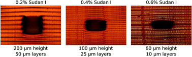
Microfluidics imposes different requirements on 3D printing compared to many applications because the critical features for microfluidics consist of internal microvoids. Resins for general 3D printing applications, however, are not necessarily formulated to meet the requirements of microfluidics and minimize the size of fabricated voids. In this paper we use an optical approach to guide custom formulation of resins to minimize the cross sectional size of fabricated flow channels as exemplars of such voids. We focus on stereolithography (SL) 3D printing with Digital Light Processing (DLP) based on a micromirror array and use a commercially available 3D printer. We develop a mathematical model for the optical dose delivered through the thickness of a 3D printed part, including the effect of voids. We find that there is a fundamental trade-off between the homogeneity of the optical dose within individual layers and how far the critical dose penetrates into a flow channel during fabrication. We also experimentally investigate the practical limits of flow channel miniaturization given the optical properties of a resin and find that the minimum flow channel height is ∼3.5–5.5 ha where ha is the optical penetration depth of the resin, and that the minimum width is 4 pixels in the build plane. We also show that the ratio of the build layer thickness to ha should be in the range 0.3–1.0 to obtain the minimum flow channel height for a given resin. The minimum flow channel size that we demonstrate for a custom resin is 60 μm × 108 μm for a 10 μm build layer thickness. This work lays the foundation for 3D printing of <100 μm microfluidic features.
1 Introduction
As discussed in ref. 1, the last few years have seen a steep increase in publications involving 3D printing of fluidic networks in cm-scale devices. This is indicative of growing interest in 3D printing for rapid prototyping of fluidic devices in which devices are fabricated layer-by-layer directly from a 3D CAD design. A particularly promising 3D printing method for fluidics is stereolithography (SL) based on Digital Light Processing (DLP). In this approach a micromirror array is used to optically define the pattern for an individual layer by selective photopolymerization of a photo-sensitive resin. Successive layers of resin are exposed with appropriate optical patterns to fabricate an entire device.1–4
For successful 3D printing, the critical aspect of fluidic devices is that they consist primarily of a series of small (micro) voids inside the polymerized material. These voids form a variety of structures including passive components5–7 such as flow channels, splitters, mixers, reaction chambers, and droplet generators, and active components such as valves8,9 and pumps.9 Note that this emphasis on small voids is in direct contrast to many typical 3D printing applications in which external features10,11 or sparse structures3 are important.
Commercial resins tend to be formulated for general 3D printing applications rather than focused specifically on the needs of microfluidic devices,12,13 i.e., small voids. Hence the smallest flow channel cross sectional dimensions reported to date are 250 μm × 250 μm,6 400 μm × 400 μm,7 and 500 μm × 500 μm.5 In our own work with an unoptimized custom resin, we have fabricated 250 μm × 350 μm flow channels.8 As discussed in Section S1 and shown in Tables S1 and S2, ESI,† in September 2015 we evaluated the minimum flow channel size that can be fabricated at four commercial 3D printing service bureaus. Only one service specifies a minimum flow channel size (500 μm × 500 μm). We found that they and another service were successful in printing channels as small as 350 μm × 350 μm with our test design. In all cases except for our own work, commercial resins were used. Importantly, these features are in the milli-fluidic, rather than microfluidic size range, such that a critical need exists to develop methods to significantly reduce 3D printed microchannel sizes.
In this paper we focus on custom formulation of resins that enable much smaller flow channels to be realized. Specifically, we develop a mathematical model for the total optical dose delivered as a function of depth through a 3D printed device, including void regions, and use it to guide the formulation of custom resins. We develop guidelines for minimum achievable flow channel size given a resin's optical properties, and demonstrate reliable fabrication of flow channels as small as 60 μm × 108 μm. Our analysis indicates how to achieve even smaller dimensions. In addition, we apply our results to an open source and several commercial resins and find good agreement with our model's predictions.
2 Experimental
2.1 3D printer
We use an Asiga Pico Plus 27 3D printer to fabricate devices and test our resins. It has 27 μm resolution in the X–Y plane and the Z-axis layer thickness can be set in 1 μm increments (i.e., 9 μm, 10 μm, 11 μm, etc.). The optical engine appears to be based on a Texas Instruments (TI) DLP4500 module, which has a 912 × 1140 micromirror array in a diamond pixel orientation. Each test part is rotated 45° on the build platform so that it aligns with the diamond orientation of the pixels (see Fig. 1). This ensures that flow channel widths can be sized as an integer number of pixels to unambiguously determine the minimum channel width that can be successfully fabricated.
 |
| Fig. 1 Schematic illustration of device orientation and imaged DLP pixels on 3D printer build platform. | |
2.2 Materials
Resins for SL DLP 3D printing generally consist of one or more monomer materials, a photoinitiator, and an absorber, where the latter is used to control the penetration depth of the incident light. For our resins, the monomer, photoinitiator, and absorber are, respectively, poly(ethylene glycol) diacrylate (PEGDA, MW 258), phenylbis(2,4,6-trimethylbenzoyl)phosphine oxide (Irgacure 819), and Sudan I. We have previously shown14 that polymers formed from this molecular weight PEGDA result in a microfluidic material that is long-term stable in water. PEGDA and Sudan I were purchased from Sigma-Aldrich (St. Louis, MO), while Irgacure 819 was procured from BASF (Vandalia, Illinois). All materials were used as received. Resins were prepared by mixing 1% (w/w) Irgacure 819 in PEGDA along with a variable amount of Sudan I (0.05%, 0.1%, 0.15%, 0.2%, 0.4% or 0.6% w/w), and sonicating for 30 minutes. Resin containers were wrapped in aluminum foil to protect the resin from light.
For comparison, two commercial resins were acquired and tested: PlasClear (made by Asiga and sold by Proto Products, Fairview, TN) and FSL Clear (Full Spectrum Laser, Las Vegas, NV). We also mixed and tested an open source resin, PR48, from Autodesk's Ember 3D printing project.15 For this resin, di(trimethylolpropane)tetraacrylate (DTPTA), trimethylolpropane ethoxylate triacrylate (TPET), 2-[[(butylamino)carbonyl]oxy]ethyl acrylate (BACA), and 2,5-bis(5-tert-butyl-benzoxazol-2-yl)thiophene (TBT) were purchased from Sigma-Aldrich and ethyl(2,4,6-trimethylbenzoyl)phenylphosphinate (TPO), was purchased from Combi-Blocks (San Diego, CA). PR48 resin was prepared with 24g each of DTPTA and TPET and 12g of BACA along with 96 mg (0.16% w/w) of the optical absorber, TBT, and 0.24g (0.4% w/w) of the photoinitiator, TPO. This mixture was sonicated in an amber glass container for at least 20 minutes to ensure thorough mixing, following which the container was wrapped in aluminum foil. Resin viscosities are given in Table 1.
Table 1 Resin viscosities
Resin |
Viscosity (cP) |
Ref. |
PEGDA |
57 |
16 |
PlasClear |
1262 |
15 |
FSL Clear |
700 |
17 |
PR48 |
286 |
15 |
2.3 Resin optical absorbance
Successful SL DLP 3D printing requires that the absorption spectrum of both the photoinitiator and absorber be matched with the emission spectrum of the 3D printer optical source. We used a QE65000 spectrometer from Ocean Optics (Dunedin, FL) to measure the absorbance of each resin and the 3D printer optical source spectrum. Resin absorbance measurements were made with 80 μm thick cells filled with liquid resin illuminated by attenuated light from an XCITE-120Q source (Lumen Dynamics, Ontario, Canada). The optical dose for each measurement was low enough that resin polymerization was not observed post-measurement.
Fig. 2 shows the emission spectrum of the 3D printer LED (dashed line). It has a peak at 412 nm and a FWHM of 25 nm. The figure also shows the absorbance of various resins. The dotted line is for PEGDA with 1% Irgacure 819 and no Sudan I, such that it is essentially the absorbance of Irgacure 819. Note that it has some overlap with the 3D printer source spectrum, which indicates that the LED light can activate the photoinitiator. The 0.1% and 0.4% Sudan I curves show the absorbance when different amounts of Sudan I are added to 1% Irgacure 819 in PEGDA. The Sudan I absorption dominates the resin absorbance in the wavelength range of the LED.
 |
| Fig. 2 Measured resin absorbance compared with Asiga 3D printer LED emission spectrum for several commercial and custom PEGDA resins. The 1% Irgacure curve is the absorbance of PEGDA mixed with 1% (w/w) Irgacure 819 photoinitiator. The Sudan I resins contain both Sudan I and 1% (w/w) Irgacure 819. | |
For the commercial resins, the PlasClear absorbance spectrum partially overlaps the 3D printer source spectrum. The PlasClear spectrum is likely dominated by the absorber in its resin formulation so it is not clear how much spectral overlap there is with its photoinitiator and the LED. The PR48 spectrum is very similar to the PlasClear spectrum, so it is likely that they use the same or closely related absorbers. The spectrum of the FSL Clear resin has the least overlap with the 3D printer source spectrum and would likely work better with a source that has a shorter wavelength.
2.4 Flow channel flushing
Immediately after 3D printing, un-solidified resin must be flushed from flow channels in the fabricated part. The process we use is to first rinse the part with isopropyl alcohol (IPA), followed by a ∼5 min soak in IPA, and then blow dry with nitrogen. Care is taken to blow nitrogen through both sides of the flow channels.
3 Resin optical analysis
In this section we develop a simple mathematical model for the optical dose delivered to a photopolymerizable resin during a single exposure to introduce the concepts, notation, and material parameters that will be used in the more extensive model developed in Section 4. We discuss our experimental method to obtain material parameters for each of the resins introduced in Section 2 and our results.
3.1 Mathematical model
As illustrated in Fig. 3, consider a photopolymerizable resin that occupies the half-space z ≥ 0 and has absorption coefficient α with units of μm−1. Assume light is incident from z < 0 and propagates in the +z direction. Just inside the resin at z = 0 the optical irradiance is I0. The irradiance for z ≥ 0, I(z), in units of W cm−2 is given by the well-known Beer's law18 where we define the characteristic penetration depth as ha = 1/α: |
 | (1) |
 |
| Fig. 3 Schematic illustration of Beers law and definition of ha. See text for details. | |
The corresponding dose, D(z, t), in units of J cm−2 for an exposure time of t is
|
 | (2) |
For a photopolymerization process, we define the critical dose, Dc, as the dose at which polymerization of the resin has proceeded far enough to result in a solid or nearly solid material. It's particular value is specific to a given resin and the spectral properties of the optical source. We can express the critical dose at some distance z = zp as
|
Dc = tpI0 e−zp/ha,
| (3) |
where
tp is the time it takes to reach the critical dose at the depth
zp. Therefore
zp represents the polymerization depth for an exposure time of
tp. Note that in general
tp and
zp represent a family of paired values for which the above equation is true (
i.e., picking the exposure time
tp sets the polymerization depth
zp and
vice versa). We can define the critical time,
Tc, as the time it takes to reach the critical dose for an optical irradiance of
I0, which can be expressed as
|
 | (4) |
Using this definition, we solve eqn (3) for the polymerization depth, zp, as
|
 | (5) |
or, in unitless parameters,
ζ =
z/
ha and
τ =
t/
Tc,
|
ζp = ln τp
| (6) |
The polymerization depth, zp, is shown for a variety of ha values in Fig. 4a. Note that when τp = 1, zp = ζp = 0 regardless of ha. In other words, when the exposure time is Tc, the resin at z = 0 receives just enough dose to become solidified, but resin at z > 0 does not. Moreover, when the resin is exposed for some τp ≥ 1, the resin at z = 0 receives a dose that is τp times larger than the critical dose, Tc. For example, if τp = 5, then ζp = ln
5 = 1.6 such that zp = 1.6 ha and at z = 0 the resin receives 5 times the critical dose.
 |
| Fig. 4 (a) Polymerization depth, zp, of resins with different ha as a function of the normalized layer exposure time, τp (eqn (5)). (b) Normalized dose as a function of depth, z, for different values of ha and the normalized exposure time, τ. | |
From eqn (2) and (4) the normalized dose, Ω(z, t), can be expressed as
|
 | (8) |
or in unitless parameters
|
Ω(ζ, τ) = τ e−ζ.
| (9) |
When
Ω ≳ 1, the resin receives enough dose to be solidified. Again, when
ζ = 0 the normalized dose is
τ.
In Fig. 4b we plot the normalized dose as a function of z for several values of ha and τ. For ha = 100 μm and τ = 2, the polymerization depth, zp, (at which the normalized dose is 1) is 68 μm. For ha = 50 μm the normalized exposure time must be twice as long to obtain the same polymerization depth, and the corresponding dose at z = 0 is of course twice as large. The obvious point is that a longer exposure time is required to reach a given polymerization depth as ha is reduced, and the inhomogeneity of the dose in the polymerized layer is increased. On the other hand, while larger ha values need shorter exposure times, the material beyond the polymerization depth receives a larger dose than for smaller values of ha, even with the shorter exposure times. This fundamental tradeoff has significant consequences for minimizing flow channel height in a 3D printed microfluidic device, which we explore in Section 4.
3.2 Measurement of ha and Tc
According to our model, the optical properties of a particular resin are determined by ha and Tc. Fortunately, these are straightforward to obtain experimentally by simply measuring the thickness of a polymerized layer as a function of exposure time and fitting the results to eqn (5). The device design we use to determine ha and Tc is shown in Fig. 5a. There are 6 single layer membranes along the forward edge of the device, each supported by 4 pillars. A typical 3D printed device is shown in Fig. 5b, and a membrane in Fig. 5c. As expected, the membrane is thicker than the build layers visible in the adjacent posts since the layer exposure time must be as long or longer than the time it takes the polymerization front to reach the previously built layer (so that the new layer attaches to the previous layer).
 |
| Fig. 5 (a) CAD design and (b) photo of 3D printed sample for determining ha and Tc. (c) Microscope photograph of membrane for 0.2% Sudan I resin with 2 s layer exposure time and 50 μm build layer thickness. The posts on which the membrane layer is fabricated are 5 layers tall. | |
For each resin, a series of samples are 3D printed with different layer exposure times, and the thicknesses of the 6 membranes on each sample are measured and averaged. The average membrane thicknesses and associated curve fits are shown in Fig. 6a as a function of layer exposure time. Values of ha and Tc are given in Table 2. Note that ha is the slope of the fitted line whereas Tc is the line's intercept with the x-axis.
 |
| Fig. 6 (a) Measured membrane thicknesses for different resins along with curve fits of eqn (5). Corresponding values of ha and Tc are in Table 2. Error bars are present for individual measurements but are generally too small to see. (b) ha of Sudan I resins as a function of Sudan I concentration. (c) Microscope photograph of membrane of 0.2% Sudan I resin with 0.45 s exposure time and 10 μm build layer thickness. The measured membrane thickness is 10 μm. | |
Table 2 ha and Tc from membrane measurements
Resin |
ha (μm) |
Tc (s) |
0.05% Sudan I |
119.2 |
0.298 |
0.1% Sudan I |
80.8 |
0.379 |
0.15% Sudan I |
57.5 |
0.395 |
0.2% Sudan I |
33.4 |
0.336 |
0.4% Sudan I |
17.5 |
0.604 |
PlasClear |
123.0 |
0.428 |
FSL Clear |
322.1 |
0.459 |
PR48 |
80.2 |
0.656 |
FSL Clear has by far the largest ha, which is due to the small overlap of its absorbance spectrum with the 3D printer source spectrum (Fig. 2). The ha for PlasClear and 0.05% Sudan I are comparable, as is ha for PR48 and 0.1% Sudan I. Increasing the Sudan I concentration decreases the penetration depth, ha. The functional relationship between the two is given by
where
ε is absorptivity and
C is concentration since, according to Beer's law,
α =
εC.
Fig. 6b shows
ha as a function of Sudan I concentration along with a fit to
eqn (10).
Knowledge of ha and Tc for a particular resin allows one to use the mathematical model to calculate a reasonable starting point for exposure parameters to create a specific structure. For example, to fabricate a 10 μm thick membrane using 0.2% Sudan I resin the model predicts a 0.45 s exposure time. The fabricated result is shown in Fig. 6c in which the membrane thickness is indeed 10 μm.
4 Resin optical properties and flow channel formation
Consider the layer-by-layer fabrication of a simple 3D printed microfluidic device with a single flow channel as schematically illustrated in Fig. 7. In A–C the part is shown being built upside down with light incident from the bottom through a window in the resin tray to expose each layer. The final part is shown right side up in Fig. 7D. The interfaces between build layers are indicated by dashed lines, and the layer indices are shown to the left in each drawing. Note in Fig. 7B that when layer 5 is formed, the flow channel region of the layer is unexposed, leaving the resin in that region in a liquid state. Likewise, exposure of layer 6 leaves the same region unexposed. Exposure of layer 7 creates the top of the flow channel, and also traps liquid resin in the flow channel (which must be flushed after fabrication). In general, the trapped resin receives some optical dose during layer 7's exposure because layer 7 does not absorb all of the incident light. Similarly, the trapped resin receives further optical doses as subsequent layers are exposed. If the sum of these doses is ≳Dc, the trapped resin can solidify and block the channel. A flow channel must therefore be tall enough to avoid this situation, which sets the optical constraint for the minimum flow channel height that can be fabricated for a given resin.
 |
| Fig. 7 Layer-by-layer fabrication process for a simplified device. The device is rotated 180° in (D) relative to (A–C). See text for details. | |
In this section we develop a mathematical model to determine the total optical dose delivered within each layer. We use the model to examine the dose when fabricating a flow channel, and analyze the effects of ha and changing the build layer thickness.
4.1 Mathematical model – multiple exposures
Let z = 0 be the plane that defines the bottom of the device being printed (see Fig. 7D). Let zl be the build layer thickness and In(z) the irradiance during exposure of layer n. We can write In(z) as |
In(z) = I0 e−[(n+1)zl−z]/ha
| (11) |
where (n + 1)zl is the position of the top of the nth layer, and n ∈ [0, N − 1] with N being the total number of layers in the device. The corresponding dose, Dn(z, t), for a layer exposure time of tl (assumed to be the same for all layers) is |
 | (12) |
The normalized dose is
|
 | (13) |
where
ζl is the normalized layer thickness,
zl/
ha. If we define
γ =
z/
zl (
i.e., normalize
z by the layer thickness) we can rewrite the normalized dose in layer
n as
|
Ωn(γ, τl) = τl e−[(n+1)−γ]ζl
| (14) |
Note that this is only valid for
|
 | (15) |
(
i.e.,
z ≤ top of current build layer) so we write the normalized dose for layer
n as
|
 | (16) |
The dose for layer
n only affects layer
n and earlier layers, but not subsequent (as-yet unbuilt) layers.
Note that the normalized dose for a given layer at the back (γ = n) and front (γ = n + 1) of a layer are
|
Ωback = τl e−ζl
| (17) |
|
 | (18) |
respectively. To have a successful 3D print, the entire layer must be polymerized,
i.e.,
Ωback ≥ 1. The minimal requirement is
in which case the normalized dose at the front of the layer is
The total dose throughout the thickness of the 3D printed part,
Ω, is just the sum of the individual layer doses,
|
 | (21) |
where
Ωn(
γ,
τl) is given by
eqn (16).
To illustrate the main features of eqn (21), consider the 5-layer case shown in Fig. 8a in which ζl = 0.69 and the normalized layer exposure time, τl, is 2.0 such that Ωback = 1.0 (which satisfies the condition in eqn (19)) and Ωfront = τl = 2.0. Note that the total dose in layers 0–3 is affected by the exposure of subsequent layers. For example, the normalized dose at the back (z = 0 μm) and front (z = 50 μm) of layer 0 is 2.0 and 3.9, respectively, while the dose at the back (z = 200 μm) and front (z = 250 μm) of the last layer (layer 4) is 1.0 and 2.0 since it receives only one exposure. Also note that in each of the layers there is significant dose inhomogeneity, which will likely affect the internal stress of an actual 3D printed part.
 |
| Fig. 8 (a) Normalized dose as a function of depth, z, for five 3D printed layers. Each layer receives a single exposure. Solid line indicates total dose. See text for details. (b) Normalized dose as a function of normalized depth, γ, for a 12-layer case with a flow channel in layers 5 and 6 (red and black layer index numbers along the top indicate exposure or no exposure in that layer, respectively). (c) Effect of layer thickness on total normalized dose. The first 200 μm represents a flow channel such that layers in this region are not exposed. | |
4.2 Total dose with an embedded channel
The total normalized dose in eqn (21) is a function of depth, γ, in the 3D printed part. So far we have assumed that every layer receives an exposure. However, when a flow channel is formed, there is no exposure in the region of each layer in which the flow channel is situated. We can account for this by defining a parameter for each layer, n, |
 | (22) |
such that the total normalized dose, Ω, becomes |
 | (23) |
We can now substitute eqn (16) for Ωn by recognizing that for a layer with index m, exposures of layers with index < m have no effect. This is equivalent to starting the sum atwhich is the largest integer value less than or equal to γ. The total normalized dose can therefore be written as |
 | (25) |
Equivalently, we can change the summation index to n′ = n − ⌊γ⌋ such that
|
 | (26) |
with
|
Ωl(γ′) = Ωl(γ − ⌊γ⌋) = Ωback e(γ−⌊γ⌋)ζl,
| (28) |
|
 | (29) |
Note that
γ′ is in the range [0,1) and is the normalized depth within a layer, with 0 being the back of a layer and 1 the front of a layer. This coordinate is the same for every layer.
Ωl(
γ′) is the normalized dose as a function of depth in a layer for a single exposure of that layer, and is in the range [
Ωback,
Ωfront). It is also the same for every layer.
χ⌊γ⌋ is the contribution to the dose of the layer with index ⌊
γ⌋ from the current and all subsequent layer exposures. Note that
χ⌊γ⌋ is governed by
δn since
δn specifies which layers are actually exposed.
To illustrate the implications of eqn (26) for flow channel fabrication, consider a 3D printed device that has 12 layers and ζl = 0.69. We assume that all layers are exposed except layers 5 and 6, which represent a flow channel. The exposure time is the same as for Fig. 8a. The total normalized dose for the structure is shown in Fig. 8b. The normalized dose in the first 5 layers is similar to what we observe in Fig. 8a (the differences are due to the additional dose from subsequent layer exposures). The normalized dose in the last 5 layers is identical to Fig. 8a. The resin in the unexposed layers 5 and 6 receives some dose from the exposures of the overlying layers 6–11. The dose is high enough to polymerize the resin in layer 6, and even in layer 5 the normalized dose is a significant fraction of 1. According to the discussion of Fig. 4b, an obvious way to avoid this situation is to increase the absorbance of the resin, i.e., make ha smaller, which increases ζl and the layer exposure time, τl. Once ha is set, however, successful fabrication of flow channels requires that the flow channel height is large enough that exposure of the overlying layers does not overly polymerize resin in the flow channel region.
4.3 Effect of build layer thickness
For a given resin which has a particular value for ha, changing the build layer thickness, zl, changes ζl. Larger ζl results in less light getting through the current build layer to further expose underlying layers. However, a larger ζl has some negative consequences as illustrated below.
As an example, consider a 200 μm tall flow channel in 0.2% Sudan I (ha = 33.4 μm) with build layer thicknesses of 10, 25, and 50 μm. The corresponding number of build layers spanned by the flow channel is 20, 8, and 4, respectively. In all cases we set Ωback = 1. As shown in Fig. 8c, the 50 μm build layer case (ζl = 1.5) has minimal penetration of the critical dose (Ω = 1) into the flow channel region. However, the variation of dose within individual layers is large (>400%), which can result in significant internal stress. Moreover, the front of each layer is so exposed (Ωfront = 4.47) that there are not as many available sites for polymer in the next layer to crosslink with, which reduces layer-to-layer adhesion. When the build layer thickness is decreased to 25 μm (ζl = 0.75), the dose variation within individual layers is reduced to ∼100% at the cost of a little more penetration into the flow channel. A build layer thickness of 10 μm (ζl = 0.3) results in greater penetration of the polymerization front into the flow channel (∼50 μm) but with only ∼25% dose variation within each exposed layer. Moreover, the average dose in each layer is nearly twice as large as for the 25 and 50 μm build layer cases, which results in a greater degree of crosslinking and likely greater internal strength.
As illustrated by this example, there is a trade-off between dose inhomogeneity within individual build layers and penetration of the polymerization front into the flow channel region. In the next section we experimentally evaluate different layer thicknesses with resins having a variety of ha values to determine practical limits to flow channel miniaturization.
5 Experimental results and discussion
To evaluate the practical limits of flow channel size as a function of ha and build layer thickness, we fabricate a series of channels through the 1.08 mm thick rectangular block that comprises the back of the device in Fig. 5a. The length of the channels is deliberately kept short to minimize the effect of flushing un-solidified resin from the channels after fabrication. Any difficulty in flushing this resin would obscure limitations to flow channel size imposed by the optical properties of the resin, which is the focus of this paper.
We first consider fabrication of flow channels for the 200 μm high channel modeled in Fig. 8c in 0.2% Sudan I PEGDA resin. The results are shown in the microscope photos of Fig. 9. For the 50 μm build layer case, the vertical edges of the flow channel are serrated with the top of each layer jutting into the channel more than the bottom. This is due to the top of a layer receiving a much larger dose than the back of the layer such that polymerization does not extend all the way to the back of the layer at the edge. Moreover, somewhat counterintuitively, channels built with this layer thickness are sometimes clogged. The 25 μm build layer case in Fig. 9b shows much less edge serration and no channels showed signs of clogging. Likewise, 10 μm build layers (Fig. 9c) improve the sidewall smoothness still further and all channels are open.
 |
| Fig. 9 Flow channels 200 μm high by 5 pixels (135 μm) wide with 0.2% Sudan I resin for build layer thicknesses of (a) 50 μm, (b) 25 μm, and (c) 10 μm. Layer exposure times, tl, are 1.5 s, 0.71 s, and 0.45 s, respectively. | |
The top of each flow channel is the back surface of an exposed layer. In Fig. 9a and b these surfaces are visibly rough, whereas in Fig. 9c it is much smoother. Evidently, smaller ζl results in smoother surfaces over the top of voids. In addition, in Fig. 9b and more so in Fig. 9c there are vertical lines on the face of the 3D printed surface. These are due to wear of the teflon film on the bottom of the resin tray that is induced by the 3D printer's slider. This wear is a major reason for periodically needing to use a fresh tray. Finally, in each photo the horizontal build layers above and below each channel are visibly bowed, as are the vertical channel boundaries. This bowing is due to stress in the 3D printed part being relieved as the channel terminates at the part's exterior surface.
Table S3, ESI,† shows similar microscope photos for flow channels with 5 pixel (135 μm) widths and channel heights of 100, 150, 200, and 250 μm and 10, 25, and 50 μm build layers for PEGDA resins with Sudan I concentrations of 0.1%, 0.15%, 0.2%, and 0.4%. Multiple 3D printed parts were made, each with multiple flow channel sizes. The number of both unclogged and total attempted fabricated channels for each combination of geometry and resin are shown on the photos to give an informal measure of yield for each channel size. The exposure parameters and normalized layer thicknesses are given in Table S4, ESI.† In each case the layer exposure time is initially set such that the calculated Ωback is 1, and then adjusted as needed until parts are successfully printed. In several cases larger channel heights were made, but the results are not included in Table S3, ESI.† The minimum flow channel heights, Hmin, fabricated with 100% yield for the resins are 100, 200, 200, and 300 μm, respectively, for the cases shown in Table S3, ESI.†
From the table, the resin with the smallest ha clearly leads to the smallest channel height. To explore this further for 0.4% Sudan I resin, consider Table 3, which shows fabricated channels as a function of channel height and width. Channel width is given in pixels (i.e., number of micromirrors in the DLP micromirror array). A pixel in the plane of the build layer is 27 μm square. Unsurprisingly, a width of 2 pixels never results in open flow channels, whereas a 3 pixel width is sometimes successful. We expect this is due to the fidelity of the image formed in the build plane by the projection optics. The minimum pixel width to guarantee 100% yield is 4 pixels (108 μm). We find this to be true for all Sudan I PEGDA resins that were tested except those with larger ha, in which case a width of 5 pixels is needed. From Table 3 the minimum flow channel height for 100% yield for 0.4% Sudan I is 90 μm.
Table 3 Channels in 0.4% Sudan I resin as a function of width and height for tl = 0.8 s and zl = 10 μm (ζl = 0.57)
Width |
Channel height |
70 μm |
80 μm |
90 μm |
2 pixels |
 |
 |
 |
3 pixels |
 |
 |
 |
4 pixels |
 |
 |
 |
5 pixels |
 |
 |
 |
6 pixels |
 |
 |
 |
7 pixels |
 |
 |
 |
8 pixels |
 |
 |
 |
9 pixels |
 |
 |
 |
To decrease the flow channel height still further we created a 0.6% Sudan I PEGDA resin. Since the absorption is very high we found it problematic to accurately measure ha using the method described in Section 3.2. Instead, we used the curve fit in Fig. 6b to estimate ha as 11 μm. Results are shown in Table 4. As with 0.4% resin, the minimum channel width is 4 pixels. For 100% yield the minimum channel height is 60 μm. The corresponding cross sectional area is 20 times smaller than our results for commercial 3D printing service bureaus.
Table 4 Channels in 0.6% Sudan I resin as a function of width and height for tl = 1.55 s and zl = 10 μm (ζl = 0.91)
Width |
Channel height |
50 μm |
60 μm |
70 μm |
80 μm |
90 μm |
3 pixels |
|
 |
 |
 |
 |
4 pixels |
 |
 |
 |
 |
 |
5 pixels |
 |
 |
 |
 |
 |
6 pixels |
 |
 |
 |
 |
 |
7 pixels |
 |
 |
 |
 |
 |
8 pixels |
 |
 |
 |
 |
 |
9 pixels |
 |
 |
 |
 |
 |
From the trends observed in our flow channel results, there is a clear path to fabricate even smaller flow channels. To reduce flow channel height, the resin absorbance must be increased to obtain smaller ha. The build layer thickness also needs to be reduced accordingly. To decrease the channel width, the x–y pixel size must be smaller so that a 4 pixel feature is commensurately reduced in size while maintaining high image fidelity. This means the DLP micromirror array must be imaged with smaller magnification optics, which in turn reduces the x–y build area. To compensate, larger pixel count DLPs need to be used such as the 1920 × 1080 pixel DLP6500 or 2560 × 1600 pixel DLP9000.
The yield as a function of flow channel height is plotted in Fig. 10a for the various Sudan I PEGDA resins used in this study, and for the build layer thicknesses that gave the smallest flow channels results. Note that the normalized layer thickness, ζl, for each case is between ∼0.4 and ∼0.9. Other than the 0.15% and 0.2% Sudan I resins, increasing absorber concentration (decreasing ha) leads to smaller flow channel heights, with the smallest being 60 μm. Alternatively, yield data from all of the Sudan I PEGDA resins can be plotted as a function of the normalized channel height, Hmin/ha, and normalized layer thickness as shown in Fig. 10b. The data can be summarized with the following observations. Minimum flow channel heights occur for 0.3 ≤ ζl ≤ 1. In resins with ha ≳ 50 μm the minimum flow channel height is ∼3.5 ha, while for resins with ha ≲ 40 μm it is ∼5.5 ha. At this point it is unclear why these are different and further investigation is warranted.
 |
| Fig. 10 (a) Minimum flow channel height with 100% yield for PEGDA resins with different Sudan I concentrations. (b) Experimental results of yield (green: 100%, yellow: partial, red: none) for normalized channel height and normalized layer thickness. | |
Results for commercial and open source resins are shown in Fig. 11. The minimum flow channel height for PlasClear is 8.1 ha. The reason it is so large is that PlasClear's high viscosity (Table 1) prevents uncured resin from being fully flushed from smaller flow channels. This is an example of something other than a resin's optical properties being the limiting factor in determining the minimum flow channel height. The designed minimum flow channel height for FSL Clear that was reliably open is ∼3.4 ha. However, since much of the channel is blocked by polymerized resin, the actual size of the opening is substantially less than the design height. For this resin we found considerable variation in the fraction of the flow channel height that is blocked. For PR48 the minimum flow channel height is 5.0 ha, which is similar to higher absorption Sudan I PEGDA resins.
 |
| Fig. 11 Smallest consistently open channels printed with commercial and open source resins. Microscope photos (a), (c), and (d) are taken with a 5× objective while (b) uses a 10× objective. The build layer thickness for (a) and (b) is 50 μm, and 100 μm for (c) and (d). | |
6 Conclusions
In summary, we have investigated the effect of resin optical properties on the minimum flow channel size that can be fabricated with SL DLP 3D printing. We have developed a mathematical model of the optical dose delivered to a 3D printed part as a function of depth for multiple exposed layers in the presence of flow channels (voids). The model shows that there is a fundamental trade-off between the homogeneity of the dose within an individual layer and how far the polymerization front extends into an underlying flow channel during fabrication. We experimentally tested the minimum flow channel size that can be fabricated by formulating custom PEGDA resins with 1% Irgacure 819 photoinitiator and a variety of Sudan I concentrations to vary the penetration depth, ha, over an order of magnitude, 11 μm to 119 μm (which is dependent on the 3D printer source spectrum). We find that the minimum flow channel height for a particular resin is typically ∼3.5–5.5 ha. The minimum channel width that can be fabricated with 100% yield is 4 pixels for our 3D printer, which is likely to be as good as or perhaps better than other SL DLP 3D printers. We experimentally determined ha for an open source and two commercial resins and found that their minimum flow channel size is consistent with our findings for the custom resins as long as the resin is not too viscous such that flow channels can be adequately flushed after fabrication. Further reductions in flow channel size should be readily achievable by increasing resin absorbance (i.e., reducing ha) and increasing the x–y plane resolution of the projected image from the DLP micromirror array. These advances should facilitate broad usage of 3D printing methods for the construction of truly microfluidic (rather than mill-fluidic) devices.
Acknowledgements
We thank the National Institutes of Health (R01 EB006124) for partial support of this work.
References
- C. M. B. Ho, S. H. Ng, K. H. H. Li and Y.-J. Yoon, Lab Chip, 2015, 15, 3627–3637 RSC
. - Y. Lu, G. Mapili, G. Suhali, S. Chen and K. Roy, J. Biomed. Mater. Res., Part A, 2006, 77, 396–405 CrossRef PubMed
. - F. P. W. Melchels, J. Feijen and D. W. Grijpma, Biomaterials, 2010, 31, 6121–6130 CrossRef CAS PubMed
. - B. C. Gross, J. L. Erkal, S. Y. Lockwood, C. Chen and D. M. Spence, Anal. Chem., 2014, 86, 3240–3253 CrossRef CAS PubMed
. - K. C. Bhargava, B. Thompson and N. Malmstadt, Proc. Natl. Acad. Sci. U. S. A., 2014, 111, 15013–15018 CrossRef CAS PubMed
. - A. I. Shallan, P. Smejkal, M. Corban, R. M. Guijt and M. C. Breadmore, Anal. Chem., 2014, 86, 3124–3130 CrossRef CAS PubMed
. - A. K. Au, W. Lee and A. Folch, Lab Chip, 2014, 14, 1294 RSC
. - C. I. Rogers, K. Qaderi, A. T. Woolley and G. P. Nordin, Biomicrofluidics, 2015, 9, 016501 CrossRef PubMed
. - A. K. Au, N. Bhattacharjee, L. F. Horowitz, T. C. Chang and A. Folch, Lab Chip, 2015, 15, 1934–1941 RSC
. - C. Schubert, M. C. van Langeveld and L. A. Donoso, Br. J. Ophthalmol., 2014, 98, 159–161 Search PubMed
. - T. L. Gerstle, A. M. S. Ibrahim, P. S. Kim, B. T. Lee and S. J. Lin, Plast. Reconstr. Surg., 2014, 133, 446–451 CrossRef CAS PubMed
. - P. N. Nge, C. I. Rogers and A. T. Woolley, Chem. Rev., 2013, 113, 2550–2583 CrossRef CAS PubMed
. - D. Mark, S. Haeberle, G. Roth, F. von Stetten and R. Zengerle, Chem. Soc. Rev., 2010, 39, 1153 RSC
. - C. I. Rogers, J. V. Pagaduan, G. P. Nordin and A. T. Woolley, Anal. Chem., 2011, 83, 6418–6425 CrossRef CAS PubMed
. - B. Adzima, The Ember Printer: An Open Platform for Software, Hardware, and Materials Development, uv.ev WEST Conference, Redondo Beach, CA, 2015 Search PubMed
. - Measured in our labs, 2015.
- Private communication from manufacturer, 2015.
- P. F. Jacobs, Rapid Prototyping and Manufacturing: Fundamentals of StereoLithography, McGraw-Hill, Inc., New York, NY, USA, 1993 Search PubMed
.
Footnote |
† Electronic supplementary information (ESI) available. See DOI: 10.1039/c5ra23855b |
|
This journal is © The Royal Society of Chemistry 2015 |
Click here to see how this site uses Cookies. View our privacy policy here.