Naoum Vaenasa,
Dimitrios Koniosab,
Thomas Stergiopoulosc and
Emmanuel Kymakis*a
aCenter of Materials Technology and Photonics & Electrical Engineering Department, School of Applied Technology, Technological Educational Institute (TEI) of Crete, Heraklion, 71004, Crete, Greece. E-mail: kymakis@staff.teicrete.gr
bDepartment of Chemistry, University of Crete, Heraklion, 71003, Crete, Greece
cDepartment of Chemistry, Aristotle University of Thessaloniki, 54124, Thessaloniki, Greece
First published on 15th December 2015
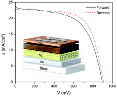
High efficient organolead trihalide perovskite solar cells typically utilize high temperature processed TiO2 as the electron transporting layer (ETL). A new method for the preparation of low temperature processed amorphous TiO2 as the ETL in planar perovskite solar cells is demonstrated. The proposed technique allowed the entire fabrication of perovskite solar cells with power conversion efficiencies as high as 13.7%, to take place at temperatures lower than 150 °C. We revealed that the source of device efficiency lies in the fast and balanced charge transport within the selective contacts as well as the effective charge extraction from the perovskite.
It is currently widely acceptable that the operation mechanism of PeSC11 is analogous to the amorphous silicon photovoltaic and not to the so-called exciton photovoltaics (dye sensitized SC, organic SC), with which the PeSC has more similarities, in both material synthesis and fabrication. The perovskite acts as an intrinsic semiconductor with increased electron and hole mobilities, while the hole and electron transport layer (HTL, ETL) stand for the p and n selective contacts, building in this way a p-i-n device.12 The exciton binding energy has been estimated in the order of some meV (≈2 meV),13 dictating that PeSCs are non-excitonic at room temperature. Another interesting point is that the photocurrent direction can be switched repeatedly in PeSC by applying a small electric voltage with opposite polarities.14 This field-switchable photovoltaic effect was recently attributed to the formation of reversible p- and n-doped areas that are induced by ion drifting across the perovskite layer.15 MAPbI3 are mixed ionic–electronic conductors with activation energies (0.6 eV) for iodide ions migration. Such ion migration has been suggested as the main reason for their unusual behavior, including current–voltage hysteresis and a giant dielectric response at low frequencies.16
Hysteresis phenomenon remains under debate, but it is believed that except ion transportation additional factors may contribute to this behavior. The ferroelectric nature of the hybrid perovskite6 is also responsible for the spontaneous electric polarization of the photoactive layer.17 Likewise, the current–voltage characteristics of a PeSC were modelled using a numerical drift-diffusion, in which the hysteresis effects were induced by including both ion migration and trapped electronic charges.18 The interface between the perovskite and the ETL is a key point in the hysteresis appearance. In many works, hysteresis is screened by the use of [6,6]-phenyl C61 butyric acid methyl ester (PC61BM) as ETL,19 owing to the passivation of interface defects and the improved electron extraction from the perovskite.20 Although, it has been revealed that cooling the device to temperature of 175 K resulting in the appearance of substantial J–V hysteresis.21 Thus, it can be concluded that changes to device architecture which claim to remove room temperature hysteresis actually do not remove the underlying processes, but rather shift them to timescales not readily observable in typical room temperature J–V scans. On top of that, PeSCs free of an ETL have also exhibited the hysteretic behavior.22 However, the highest power conversion efficiency (PCE) has been achieved in PeSCs, which utilize anatase TiO2 (an-TiO2) as the ETL.23
High temperature sintering up to 500 °C (ref. 24) or laborious methods25,26 are needed in order to convert TiO2 precursor solutions to anatase polymorphism, which has the optimum electrical properties of the other phases. Many works have demonstrated the replacement of an-TiO2, with ZnO,27 WOx,28 SnO2,28 PCBM29 and titania with different crystal phases.30 However, the majority of these materials are compatible with demanding and costly, perovskite deposition methods, as the two step31 and the evaporation,32 due to their sensitivity and consequent degradation to one step solution procurable methods.
In this work, a new method for the preparation of low temperature processed amorphous TiO2 ETL, adapted from the organic photovoltaics fabrication techniques33,34 is presented, allowing the entire device fabrication to be conducted at temperatures lower than 150 °C. PeSCs using the amorphous TiO2 ETL were fabricated, exhibiting a maximum PCE of 13.7%.
The planar PeSC devices were fabricated with a sequential deposition of each layer. For the TiO2 ETL preparation, 0.56 ml of titanium isopropoxide was first dissolved in 5 ml of isopropanol. The resultant solution was stirred for 15 min at room temperature using a magnetic stirrer to yield a homogeneous, clear and transparent solution. 20 μl of hydrochloric acid was added to the solution as a stabilizing agent (pH 1.5).35 Fresh TiO2 solution was spin coated on glass/ITO substrates at 4000 rpm for 45 s and annealed at 150 °C for 45 min. Subsequently, the mixed halide perovskite36 active layer, composed of a 40% wt solution with 3:
1 molar ratio of MAI
:
PbCl2 in DMF was spin coated at 2000 rpm for 60 s and two-step annealed at 90 °C for 2.5 h and 120 °C for 20 min. The HTL, comprised of 15 mg ml−1 poly(3-hexylthiophene-2,5-diyl) (P3HT) solution in chlorobenzene, was spin coated at 1500 rpm for 45 s.37 The devices' active area was set at 4 mm2. The whole fabrication procedure, except the ETL formation, was conducted in a N2 filled glovebox with O2 and H2O levels <0.1 ppm. Finally, the Ag anode was thermally evaporated at high vacuum 1 × 10⁻⁶ mbar. The by UV-VIS absorption spectra of the samples were recorded using a Shimadzu UV-2401 PC spectrophotometer. The morphology of the surfaces was examined by scanning electron microscopy (SEM JEOL JSM-7000F) and by atomic force microscopy (AFM; Digital Instruments NanoScope IIIa). The performances of the devices were measured at room temperature with an Air Mass 1.5 Global (A.M. 1.5 G) solar simulator at an intensity of 100 mW cm−2. A reference monocrystalline silicon solar cell from the Newport Corp. was used to calibrate the light intensity. The samples were characterized by Raman spectroscopy at room temperature utilizing a Nicolet Almega XR Raman spectrometer (ThermoScientific) with a 473 nm blue laser as an excitation source. The external quantum efficiency measurements were conducted using an integrated system (Enlitech, Taiwan) and a lock-in amplifier with a current preamplifier under short-circuit conditions.
Fig. 1a and c present the configuration of the planar PeSC and the corresponding energy levels of each layer respectively.38 According to the scanning electron microscopy (SEM) measurement the thicknesses of the device layers are: ITO 100 nm, TiO2 100 nm, CH3NH3PbI3−xClx 400 nm, P3HT 50 nm and Ag 100 nm. Fig. 1b shows a magnified SEM cross section image of the ETL and reveals that the specific method for the TiO2 development leads to the formation of a smooth compact layer, which is necessary for avoiding possible recombination among the ITO and the perovskite.39 In order to identify the crystal phase of the TiO2 layer, Raman analysis was performed.
Firstly, we reordered the substrate Raman spectrum (Fig. 1d), which demonstrates only one broad peak centered at 585 wavenumbers, then we conducted a comparative evaluation between, the used in this study, TiO2 layer annealed at 150 °C and an identical layer that has been annealed in an oven at 500 °C. The 500 °C TiO2 film presents the characteristic anatase modes (Eg, B1g, A1g)40 as expected, but the 150 °C TiO2 film does not exhibit any traces of crystalline phases, indicating an amorphous TiO2 film.41 In the next step of our study and with a view to conduct a thorough evaluation of the morphological features of the device, we carried out a comparable analysis of the SEM and AFM images (Fig. 2) after the deposition of every layer. The TiO2 film exhibited a highly homogeneous top surface Fig. 2a and d without any cracks and with very low roughness, (root mean-square) RRMS = 1.25 nm. In spite of that, after the spin coating and the annealing of the perovskite layer, the roughness increased significantly to RRMS = 30.47 nm, something that is obvious in Fig. 2b and e. We can connect the roughness augmentation with the development of large crystallites during the annealing process.42 The surface's topography was improved significantly after the spin coating of a thin (50 nm) P3HT layer (Fig. 2c and f). The roughness decreased about 30% to RRMS = 21.75 nm, also some small cracks and voids that have been shaped in the previous step, were covered by the P3HT contributing, in this way, in the establishment of an efficient interface with the largest possible active area.
![]() | ||
Fig. 2 SEM and AFM images of (a) and (d) TiO2 film, (b) and (e) TiO2 after being coated by the perovskite, (c) and (f) TiO2 with perovskite and a P3HT layer. |
Should be noted here that with a view to improve the chemical stability of the device we harnessed an undoped conducting polymer P3HT which in contradiction to Spiro-OMeTAD43 can work efficiently, without the presence of any dopants such as hydrophilic LiTFSI and volatile TBP that including in Spiro-OMeTAD. Moreover, through the Hall measurement we determined the hole mobility of P3HT to 4.47 × 10⁻² cm2 V−1 S−1, which is two order of magnitude higher than that of the undoped Spiro-OMeTAD.44 On top of that, P3HT is the right HTL for large area applications,45 since it exhibits increased stability,46 superior morphological characteristics47 and low cost.
Taking into consideration the need of PeSC for careful characterization we recorded the J–V curves of Fig. 3a, in quasi-steady-state conditions in order not to overestimate our results.48 The respective photovoltaic characteristics are summarized in Table 1. The scan rate was 10 mV s−1 and we neither light soaked the cells nor pre-biased them before the measurement with respect not to polarize the perovskite layer. To check the reproducibility of the performance of the planar perovskite solar cells using the amorphous TiO2 ETLs, fifty devices were prepared and characterized, the average PCE is about 11.5% and the short-circuit current and open-circuit voltage exhibited elevated values 23 mA cm−2 and 900 mV respectively, revealing the proper operation of the active layer. The champion device exhibited a PCE of 12.3% and 13.7% under forward and reverse bias respectively. The positive affection of the proposed TiO2 compact layer was confirmed by the fabrication of a pristine device without any ETL. The pristine device exhibits a very poor PCE of 3.16%, presumably due to an unfavorable electronic contact forming at the ITO perovskite. Therefore, the significant PCE increase upon the utilization of an amorphous TiO2 as the ETL can be attributed to a cumulative action of factors, including good charge transport at the ETL/perovskite interface due to the high compactness of the TiO2 and the high electron mobility of the TiO2, which prevents the electron recombination, since the calculated series resistance (Rs) from current–voltage (J–V) curve is as low as 6.5 Ω cm2. However the FF reaches a reasonable value, from 0.58 to 0.65, only when a reverse scan was performed (Fig. 3a).
![]() | ||
Fig. 3 (a) Characteristic J–V curves and corresponding electrical features of PeSCs for forward and reverse scan, (b) EQE of the PeSC device and the absorbance spectrum of the perovskite layer. |
Scan | ETL | JSC (mA cm−2) | VOC (mV) | FF | PCE (%) |
---|---|---|---|---|---|
FRW | TiO2 | 23.7 | 895 | 0.58 | 12.3 |
RVS | TiO2 | 22.6 | 910 | 0.66 | 13.7 |
Average | TiO2 | 23.0 | 900 | 0.55 | 11.5 |
Average | — | 12.4 | 788 | 0.32 | 3.16 |
Given that the Rs exhibits a normal value,37 implying that the interfacial recombination processes are decreased and the low FF (for the normal scan direction) should be interpreted in terms of an internal hindrance in the charge transport. For recording the reverse scan (1 V → 0 V), an initial high bias (1 V) is applied, which induces the drift of mobile perovskite ions. The negative ions move toward the anode and induce an n-doped area nearby to the interface with HTL. An analogous process takes place also to the cathode. Thus the fast induced polarization of the perovskite, during the reverse scan, facilitates the charges extraction to the selective contacts and increases the SC's FF. As a consequence the PCE for the reverse scan increased to 13.7%. The present but reduced8 hysteresis among the two scan directions is ascribed to the large perovskite crystalline domains48 which positively affect the charges transportation.
Fig. 3b shows the external quantum efficiency (EQE) of PeSC devices and the corresponding absorbance (Abs) of the perovskite layer. EQE is upper than 80% pointing out the elevated collection of generated carriers and the small recombination losses at short-circuit. The onset of absorbance placed at about 800 nm in good accordance with the initiating of EQE spectrum. The calculated JSC 21.5 mA cm−2 from the EQE graph was in good accordance with the J–V measured values. The optical band gap for this mixed halide perovskite derived from the Abs spectrum is about 1.55 eV. In the course of the J–V measurements we observed a peculiar behavior of the PeSC (Fig. 4a). Some repeated scans should have been monitored before reaching the maximum PCE. To the best of our knowledge this is the first time that such a phenomenon is observed. To shed light on the origin of this finding we examined separately each layer of the device. First we suspected P3HT for possible photoconductivity, but when we replaced it with undoped Spiro-OMeTAD we observed the same behavior. Then, we turned our attention to the perovskite absorbing layer and apart from the initial repeated forward scans, reverse scans with different scan rates were also recorded (Fig. 4b).
![]() | ||
Fig. 4 (a) Characteristic J–V curves recorded in forward scan till the PeSC reaches the max PCE and (b) afterwards in reverse scan with different scan rates. |
In both the forward and reverse scans, S-shaped J–V curves responsible for the photo-induced ion migration processes48 weren't traced, the only discrepancy among the scans was the expected J–V hysteresis. Eventually we focused on the TiO2 ETL and searched through literature for relevant cases. An analogous trend was observed in OPVs when sol–gel fabrication methods were applied for the preparation of inorganic ETL (ZnO, TiOx).49–51 In all these works, the solar cells exhibited an extremely slow photo-response (30–60 min) in reaching the maximum PCE. This aforementioned behavior was partially healed when the ETLs were subjected to a UV cure, which improved the charge collection efficiency of the device. In our occasion it takes only 5 min to reach the maximum PCE. The PCE remained stable even after 30 min of repeated scans (1 every min) and illumination stress. Thus, we considered that the amorphous nature of TiO2 is responsible for this behavior, by introducing electron trap states,52 which need a certain period of time before being completely filled. Having been triggered by the short loading period of 5 min, we measured the Hall mobility (Ecopia HMS-3000, at room temperature) of the TiO2 film. A high electron mobility value of 2.89 × 10⁻² cm2 V−1 S−1 similar to this of the crystalline titania was observed,26 which can be explained in terms of the high degree of compactness.
Finalizing our analysis we believe that the high and comparable values of Hall mobilities (same order of magnitude) of the amorphous TiO2 ETL and P3HT HTL account for the fast and balanced charge transport within these layers and the effective charge extraction from the perovskite, and therefore a lower carrier recombination. In this way the short charging time of Fig. 4a and the decreased hysteresis in Fig. 3a can be explained.
This journal is © The Royal Society of Chemistry 2015 |