DOI:
10.1039/C5RA23069A
(Paper)
RSC Adv., 2015,
5, 107811-107821
Synthesis of graphene oxide–silver nanocomposite with photochemically grown silver nanoparticles to use as a channel material in thin film field effect transistors
Received
3rd November 2015
, Accepted 11th December 2015
First published on 14th December 2015
Abstract
In this article we report a convenient method for synthesizing a graphene oxide (GO)–silver nanoparticle (SNP) composite and its application as a channel material in thin film field-effect transistors (TFTs). The SNPs were prepared through photochemical reduction of silver nitrate in aqueous solution using monoethanolamine (ME) as the reducing agent and sodium dodecyl sulphate (SDS) as the stabilizer. The growth of SNPs is explained with a mathematical model combining classical nucleation theory with photoinduced electron transfer theory. GO was prepared by the modified Hummer's method and SNPs were loaded to it in different concentrations for preparing the composite. The formation of composite through the ex situ process is confirmed through spectroscopic and microscopic techniques. Further, it was used as a channel layer on a SiO2/Si substrate with a Au source and a drain for the thin film TFT in the back gated configuration. The TFT shows dominant p-type field effect characteristics compared to pure GO based TFTs. The transport of charge carriers through the channel is well tuned by controlling the dose of SNPs. The field effect mobility of the charge carriers is found to vary from 2.44 cm2 V−1 s−1 to 1.10 cm2 V−1 s−1 with the increase in SNP content in GO. The transport of charge carriers occurs through the channel by Fowler–Nordheim tunneling at higher gate voltages while at lower voltages multistep charge-carrier hopping occurs. Our study provides new insights in controlling transport of charge-carriers through GO to achieve tunable electrical properties for GO based electronic devices.
Introduction
Graphene oxide (GO), a common derivative of graphene with a tunable bandgap from semimetal to semiconductor, is a promising material for large area flexible and transparent electronics.1 GO is a monolayer of graphene with attached oxygen functional groups which can be derived by oxygenating it with phenolic, carboxyl and epoxide groups on both the planes and edges.2 Due to these oxygenated groups, GO exhibits hydrophilic properties and can be dispersed in water and alcoholic solvents.3 As it has high specific area and improved loading capacity,4 it is effectively used as a matrix for metal nanoparticle composites. SNPs have been widely used to prepare GO–SNP nanocomposite to add improved functionalities to its optical and electrochemical properties5 and catalytic activities.6 As completely oxidized GO has poor electrical conductivity, it cannot be used as a channel material for field effect transistors.7
The electrical conductivity of GO can be enhanced effectively by impregnating SNPs into it. Dinh et al.8 recently reported an environment friendly method of preparing GO–SNP composite by in situ ultrasonication with citric acid and showed an enhancement in conductivity of the composite films by 40 times compared to reduced GO. Mandal et al.9 reported the application of SNPs as gate dopant for paper-pencil-based flexible field effect transistor and also showed its superiority over ionic liquid and reduced GO. Xu et al.10 have also used SNP/graphene nanohybrid as channel in ionic liquid gated field effect transistor for photodetection. However, GO–SNP composite is not studied as a channel material in GO based thin film field effect transistor and the effect of SNP concentration on its transport behavior is not studied until now.
Various methods for synthesizing stable ensemble of monodispersed silver nanoparticles have been exploited such as Brust–Schiffrin method,11,12 sonolysis,13 chemical reduction,14 microwave assisted synthesis,15 microbial method,16 laser ablation method,17,18 seed-mediated synthesis,19 surfactant-assistant reduction in polar and nonpolar solvents,20 microemulsion method,21 and electrochemical synthesis22 with typical advantages and disadvantages in each case. However, these methods are not compatible for GO composite synthesis since some methods utilize hazardous reducing agents which spoil the layered structure of graphene and some methods apply top-down strategy. Besides, in situ preparation23 for nanocomposite synthesis also requires precarious reducing agents like hydrazine, borohydrides, formaldehydes, etc.24 which complicates the process. Therefore, proper selection of chemicals such as reducing agent and surfactant for SNP synthesis is essential for preparing GO–SNP composite.
There are several reports25–28 on the photo induced growth of SNPs. Sakamoto et al.25 have described various strategies for photo reduction of different metal nanoparticles. Jradi et al.26 investigated the formation of nanosized silver particles and silver nanowires by a spatially controlled radical mediated photo reduction reaction. Sudeep and Kamat27 have studied the formation of silver nanoparticles in ethanol/toluene medium by employing thionine as a sensitizing dye. Mafune et al.28 reported the growth of size controlled silver nanoparticles by laser ablation method. Hada et al.29 investigated the formation of SNPs via the direct excitation of AgClO4 in aqueous and alcoholic solutions and proposed a formation mechanism. All the methods utilize either a photosensitizer or direct photoreduction of silver salt or photophysical reactions which are not compatible with large scale GO based composite processing. Therefore, there is still necessity for a process technology for large scale preparation and fabrication of GO–SNP composite and GO based devices. In this report, we have studied the growth of SNPs through photochemical reduction of AgNO3 with monoethanolamine (ME) as reductant and sodium dodecyl sulphate (SDS) as stabilizer. ME is a mild reducing agent which is appropriate for securing the layered structure of GO. SDS also does not disturb the attachment of GO with SNPs. The GO–SNP nanocomposite, synthesized ex situ with these SNPs, show similar kind of morphology and optical properties to that of in situ derived composites and was found to exhibit better field effect properties compared to pure GO when used as channel in thin film field effect transistors. The transport of charge-carriers has been studied in detail. Fowler–Nordheim (FN) tunneling occurs at high gate voltages whereas at low gate voltages charge carriers are transported by multistep hopping. The field-enhancement factor of FN tunneling and work function of GO–SNP composite is directly linked with the concentration of SNPs into GO. Our study confirms the validity of ex situ synthesis of GO–SNP composite and shows a convenient way to achieve tunable transport properties which is applicable to present silicon based device fabrication technology.
Experimental procedure
Growth of nanoparticles
Silver nitrate (AgNO3, 99.8%), monoethanolamine (C2H7NO) and sodium dodecyl sulphate (NaC12H25SO4) were all purchased from Merck. Deionized (DI) water was taken from Milli-Q water purification system and was used as solvent in all preparations. During synthesis, reaction parameters such as precursor concentration, duration of photo irradiation, surfactant concentration and concentration of reducing agent were varied to understand their effect on the growth. Photo irradiation was performed using a Philips 23 Watt CFL. For all the samples, reaction temperature was kept fixed at 60 °C and they were further ripened at room temperature for 2 hours. The samples were preserved under refrigeration.
Synthesis of graphene oxide and GO–SNP composite
Graphene oxide was synthesized by a widely reported Hummer's method. First graphite flakes (3 g) were oxidized using strong oxidizing agents such as NaNO3 (1.5 g) and KMnO4 (9 g) in H2SO4 (69 mL). After oxidation, the mixture was washed to obtain a neutral pH value. The mixture was then dried at 55 °C for 8 h in a vacuum to obtain graphite oxide flakes. These flakes were dispersed in DI water with a concentration of 1 mg mL−1. Three different sets of composites were prepared by mixing GO dispersion with SNP solution, viz. GO–SNP1 (GO 98 wt%, SNP 2 wt%), GO–SNP2 (GO 96 wt%, SNP 4 wt%) and GO–SNP3 (GO 94 wt%, SNP 6 wt%). After mixing, the dispersions were stirred for 24 hours to incorporate the silver nanostructure onto GO homogeneously.
Fabrication of thin-film transistors
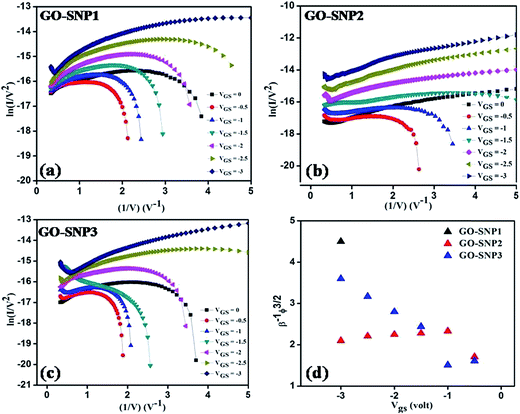
Thin-film transistors with GO–SNP nanocomposite as the channel material was fabricated by drop casting the composites onto Si/SiO2 substrate with oxide thickness of 300 μm in back gated configuration. The dispersion was dried at 120 °C under argon flow. Source and drain contacts of Au with channel length and width of 60 μm and 1200 μm respectively were fabricated by sputtering. Al gate contact was prepared on the back of Si substrate by thermal evaporation. Fig. 1 shows the schematic of the device prepared.
 |
| | Fig. 1 Schematic of the device fabricated on Si/SiO2 substrate with Au source and drain contacts and Al gate. | |
Optical measurements were carried out at room temperature using a Perkin Elmer Lambda 750 UV-Vis-NIR spectrometer taking a quartz cell (10 mm path). The particle size and morphology were observed at room temperature on a JEOL electron microscope operating at 200 kV. X-ray diffraction measurement was carried out using a Panalytical X-ray diffractometer (PW 3040/60) with Cu-Kα source with generator voltage of 40 kV and generator current of 40 mA with scanning rate of 3° min−1 at step size of 0.01°. Raman spectra were recorded in a Horiba T64000 Raman spectrometer with 514 nm laser excitation. The transfer and output characteristics of thin film transistor were recorded with Keithley 4200 SCS semiconductor parameter analyzer in voltage sweeping mode.
Results and discussion
From thermodynamic point of view the reduction of Ag+ by monoethanolamine is favored when the oxidation potential of amine falls within the reduction and oxidation potentials of silver system. For the reaction to proceed, the reduction potential of silver salt is to be lower than the oxidation potential of amine. When the amine reducing agent has an oxidation potential lower than reduction potential of Ag+, nanoparticles formation will not occur since Ag+ will not be reduced spontaneously. We assume that in the absence of light, the reducing agent remains in the unexcited state with a lower oxidation potential compared to that required to promote reduction of silver salt. In the presence of light radiation, amine goes to excited state and donates electrons to the silver system for reduction to occur.
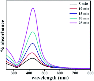
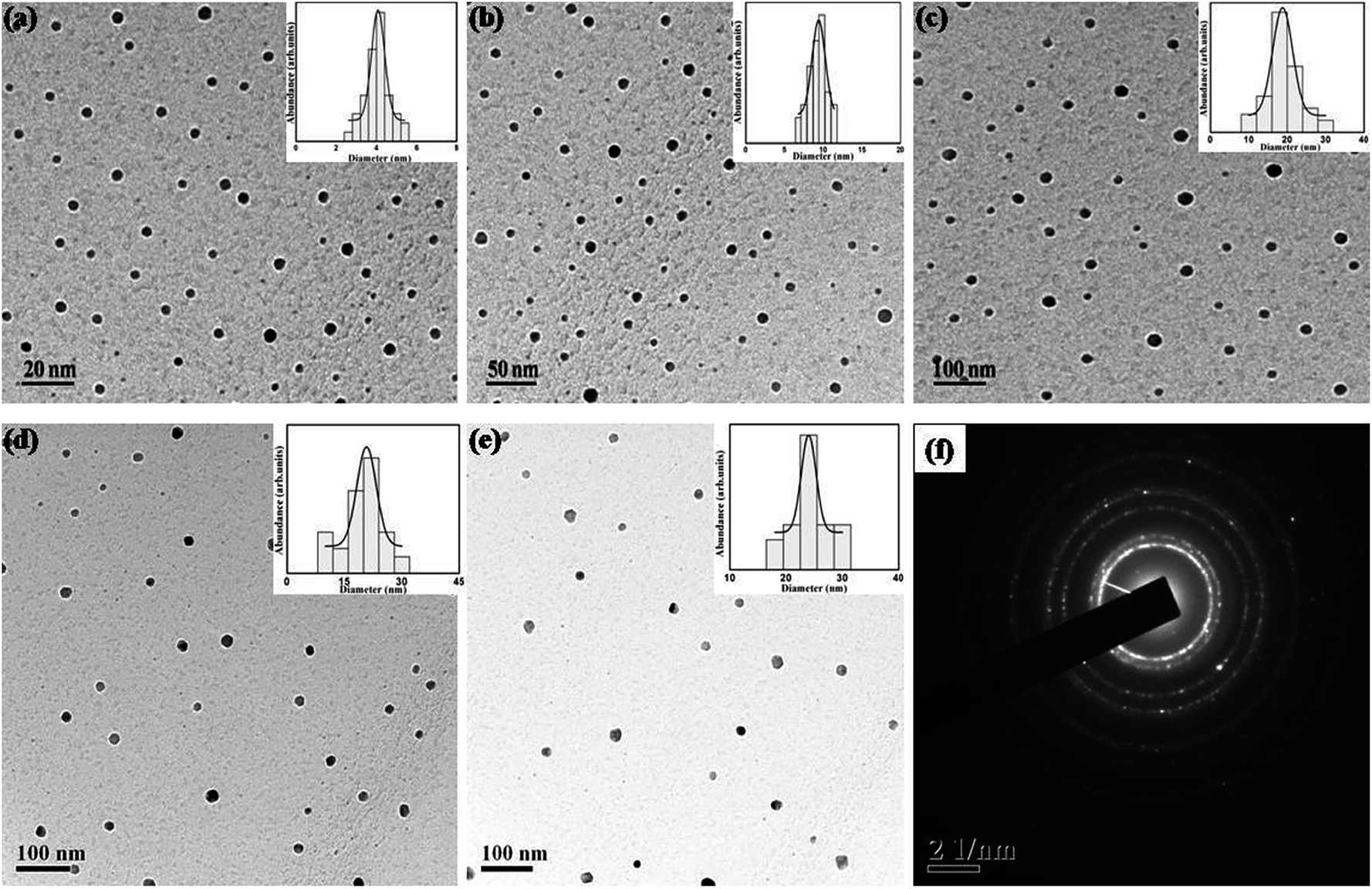
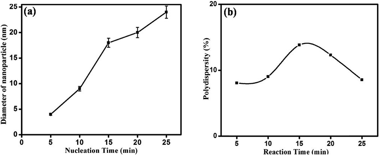
Nanoparticles were synthesized from 5 minutes to 25 minutes with 5 minutes interval keeping concentrations of precursor, reducing agent and surfactant fixed at 1 mM, 4 mM and 1 mM respectively. Fig. 2 shows the absorption spectrum of nanoparticles synthesized for different nucleation time. The spectrum taken for each of the nucleation times exhibits the characteristic surface plasmon resonance (SPR) peak around 420 nm. The occurrence of plasmon band is a result of collective oscillation of electrons in conduction band of silver which move around the particle perturbing the electron density and generating oscillation of charges under electromagnetic influence.5 Strong absorption is observed even before 5 minutes after photo-excitation indicating that nanoparticles start forming within a short period of time though a weak reducing agent is used. In contrast, weak reductant such as saccharides,30 amino acids,31 aliphatic amines,32 and citrate33 take several hours to achieve a reasonable yield of silver nanoparticles. A small red-shift of the SPR peak position is also observed with increase in reaction time. It is noteworthy to mention that gradual shift of SPR peak is accompanied by narrowing of plasmon band as shown in Fig. 2. Mie theory relates the narrowing of plasmon band with gradual increase of size of nanoparticles.34 Fig. 3 shows representative TEM micrographs of the nanoparticles and inset contains the histogram showing average size and size distribution of SNPs. Almost linear growth rate of NPs in the presence of light is observed as shown in Fig. 4a. The polydispersity indexes of NPs are calculated for every size-distribution and their variation with the size of SNPs is shown in Fig. 4b. Table 1 shows the dependence of particle size and size-distribution on the duration of irradiation in 1 mM of AgNO3 with 4 mM of monoethanolamine. The SNPs are highly monodispersed and best value of polydispersity index achieved is around 8% for 5 minutes of irradiation. Nanoparticles synthesized with longer irradiation gives slightly lower monodispersity, of course, due to the growth of particles of larger sizes. The presence of a capping layer around the SNPs is clearly visible. The color and UV-Vis spectra of SNP ensemble did not change during storage, indicating good protecting effect of SDS. This suggests that the surfactant coating on the nanoparticle surface35 prevents aggregation between neighboring nanoparticles.
 |
| | Fig. 2 Optical absorbance spectrum of SNPs synthesized with varying reaction time. | |
 |
| | Fig. 3 TEM images for SNPs synthesized for (a) 5 min, (b) 10 min, (c) 15 min, (d) 20 min, and (e) 25 min. Histogram for size distribution is shown in the respective insets. (f) SAED pattern showing polycrystalline nature of SNPs. | |
 |
| | Fig. 4 (a) Effect of reaction time on SNP average size, (b) variation of polydispersity index with duration of reaction. | |
Table 1 Dependence of particle size and size-distribution on irradiation time in 1 mM AgNO3 solution with 4 mM monoethanolamine
| Irradiation time (min) |
Diameter (nm) |
FWHM of plasmon band (eV) |
Polydispersity (%) |
| 5 |
4.07 ± 0.03 |
0.5670 |
8.07 |
| 10 |
9.41 ± 0.10 |
0.5074 |
9.03 |
| 15 |
18.77 ± 0.11 |
0.4820 |
13.83 |
| 20 |
20.80 ± 0.5 |
0.4797 |
12.30 |
| 25 |
24.02 ± 0.3 |
0.4136 |
8.54 |
The result obtained from TEM characterization agrees well with the UV-Vis spectrum. The narrowing of the plasmon band is directly related to the evolution of size of the nanoparticles.31 Nucleation and growth are two crucial phenomena that decide the final size and size-distribution in particle growth. Researchers have developed many synthetic methods based on aggregation and coalescence34 such as size focusing, digestive ripening, inverse Ostwald ripening that can provide narrow size distribution.36,37 Different synthesis protocols exhibit different kind of growth profiles. Zheng et al. and Sidhaye and Prasad recently reported about nonlinear growth rate for nanoparticle synthesis that supports conventional model for Ostwald ripening.38,39 Also aggregation process follows sigmoidal growth profile.40 However, in our system, we have observed linear growth-rate of particles. It is assumed, for this system, that only diffusion-controlled mechanisms are not the controlling factors for overall size and size-distribution; rather it is also dominated by photoinduced electron transfer process. The rate of electron transfer determines the rate of reduction of Ag+ for growth further. In the solution-phase, photoexcitation drives the molecules of monoethanolamine to excited states. The lifetime of the excited state is assumed to be long enough to encounter the Ag+ ions and consequently leads to an oxidative electron transfer reaction. The reaction undergoes in the following way:
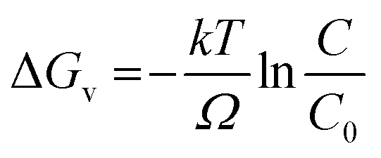
Marcus theory of electron transfer assumes that if the potential energy surfaces of initial and final states intersect with negligible electron coupling then transfer of electrons takes place at the plane of intersection. Until the source of excitation is present the reducing species lasts in reactive state maintaining a constant reaction rate. We have derived the quantitative expression for growth rate and the effect of solute concentration on SNP diameter using a model based on classical nucleation theory. The change of Gibb's free energy per unit volume of the solid phase (ΔGv) (solid phase introduced due to nucleation from solution phase) is a function of the concentration of the solute and it is expressed as
| |
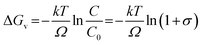 | (1) |
where
C is the concentration of the solute,
C0 is the equilibrium concentration or solubility,
k is Boltzmann constant and
T is temperature.
Ω is the atomic volume and
σ is the supersaturation defined by

.
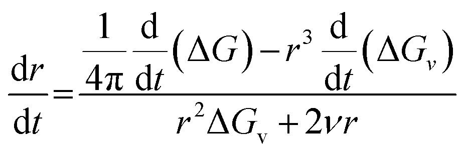
For a spherical nucleus with a radius of r, the total change of chemical potential for the formation of the nucleus, ΔG, is given by
| |
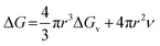 | (2) |
where
ν is the energy per unit area at SNP surface. This equation gives a static picture of the nucleation phenomenon at a specific instant of time. To add time dependence into the above equation we differentiate with respect to
t to get,
| |
 | (3) |
In the limiting case when t = t0 (i.e. the moment nucleation begins) r = r*, where r* is the critical size of nucleus and ΔG = ΔG*; where ΔG* is the critical energy barrier for nucleation.
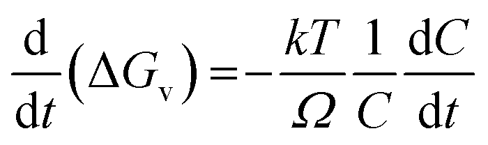
Now from eqn (1),
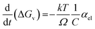
Differentiating with respect to t, we arrive at the expression,
| |
 | (4) |
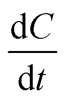
The term  in eqn (4) simply gives us the rate at which concentration of solute is reducing. In photoinduced electron transfer reactions this rate is simply equal to the rate of electron transfer (αel). Therefore, we arrive at the expression,
| |
 | (5) |
Therefore, combining eqn (3) and (5), we get
| |
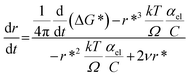 | (6) |
The rate of change of ΔG* with time is related to the rate at which solute is consumed. Constant electron transfer rate runs the reaction i.e. reduction of Ag+ at a constant rate. The denominator and the second term in the numerator of the above equation are constant for a fixed concentration of solute. Therefore the diameter of SNP increases linearly as long as constant electron transfer rate is maintained.
The effect of concentration of precursor on growth of SNPs has been evaluated in terms of morphology, size and size-distribution of nanoparticles. Fig. 5 shows the UV-Vis absorption spectrum of SNPs prepared with varying precursor concentration keeping reaction time, surfactant concentration and monoethanolamine concentration fixed at 10 minutes, 1 mM and 4 mM respectively. It is observed from the UV-Vis spectrum that with increase in precursor molarity the intensity of surface plasmon resonance around 420 nm increases along with decrease in SPR bandwidth indicating enhanced growth of nanoparticles. The narrowing of plasmon band and associated red-shift of SPR peak position indicates that the increase in precursor molarity results in NPs with increasing size.41 The effect of precursor molarity on the size and shape of nanoparticles was further characterized by TEM. Fig. 6 shows representative TEM images of synthesized NPs with their average size and size-distribution in the inset. Fig. 6f shows an almost linear increase of particle size with AgNO3 concentration. Table 2 shows the dependence of particle size and size-distribution on precursor molarity in AgNO3 solution having 4 mM of reductant and 1 mM of surfactant for irradiation of 10 minutes.
 |
| | Fig. 5 UV-Vis spectrum of silver NPs prepared with varying precursor concentration. | |
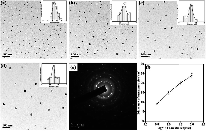 |
| | Fig. 6 TEM images for SNPs synthesized with AgNO3 concentration of (a) 0.5 mM, (b) 1 mM, (c) 1.5 mM, and (d) 2 mM. Histogram for size distribution is shown in the respective insets. (e) SAED pattern showing polycrystalline nature of SNPs, (f) effect of AgNO3 concentration on average particle size. | |
Table 2 Dependence of particle size and size-distribution on precursor molarity in solution having 4 mM of reductant and 1 mM of surfactant for irradiation of 10 min
| AgNO3 concentration (mM) |
Diameter (nm) |
FWHM of plasmon band (eV) |
Polydispersity (%) |
| 0.5 |
9.84 ± 0.37 |
0.5503 |
16.00 |
| 1.00 |
14.6 ± 0.6 |
0.4967 |
14.60 |
| 1.50 |
20.80 ± 0.5 |
0.4750 |
12.30 |
| 2.00 |
24.00 ± 0.58 |
0.4404 |
5.52 |
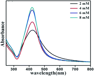
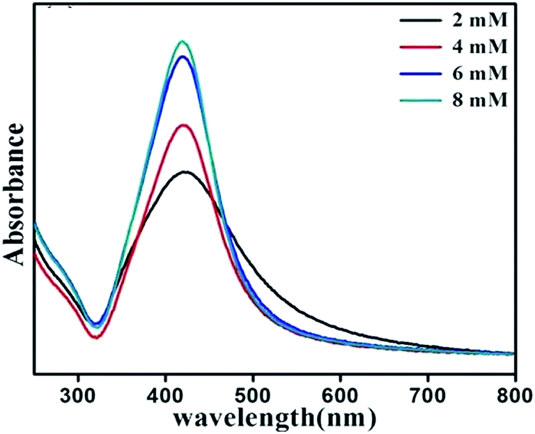
To study the effect of ME concentration, i.e. molarity of reducing agent on the shape and size of nanoparticles, 2 mM, 4 mM, 6 mM and 8 mM of ethanolamine were used for synthesis. Preparation time, AgNO3 concentration and surfactant concentration were kept fixed at 10 min, 1 mM and 4 mM respectively. Fig. 7 shows UV-Vis absorption spectrum of dispersed nanoparticles prepared with varying ethanolamine concentration. When the molarity of ME is varied from 2 to 4 mM the SPR peak is shifted slightly to lower wavelengths and does not show any further shift with the variation of molarity. However, the width of the SPR band goes on decreasing with increase in molarity of the reducing agent. Fig. 8 shows the representative TEM micrographs of nanoparticles with average size, and size-distribution in their inset; and it shows a clear linear relation between monoethanolamine molarity and size of nanoparticles. The role of ethanolamine is to reduce the Ag+ ions to promote nucleation and consequent clustering which eventually grows to particles. Higher concentration of ethanolamine in solution encounters larger population of AgNO3 molecules and leaves behind lesser amount of unreduced silver. Thus larger number of zero-valent molecules of silver (Ag0) takes part in clustering. Therefore, each cluster can incorporate more molecules than that for a solution with lower ethanolamine concentration. Table 3 shows the dependence of particle size and size-distribution on the concentration of reductant in 1 mM AgNO3 solution with 1 mM of surfactant for 10 min of irradiation.
 |
| | Fig. 7 UV-Vis absorbance spectrum of SNPs synthesized with varying monoethanolamine concentration. | |
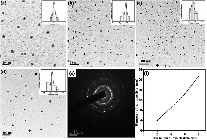 |
| | Fig. 8 TEM images for SNPs synthesized with ethanolamine concentration of (a) 2 mM, (b) 4 mM, (c) 6 mM, and (d) 8 mM. Histogram for size distribution is shown in the respective insets. (e) SAED pattern showing polycrystalline nature of SNPs, (f) effect of ethanolamine molarity on average particle size. | |
Table 3 Dependence of particle size and size-distribution on the concentration of reductant in 1 mM AgNO3 solution with 1 mM of surfactant for 10 min of irradiation
| Concentration of monoethanolamine (mM) |
Diameter (nm) |
FWHM of plasmon band (eV) |
Polydispersity (%) |
| 2 |
4.07 ± 0.03 |
0.7229 |
8.07 |
| 4 |
9.16 ± 0.27 |
0.5071 |
5.45 |
| 6 |
14.47 ± 0.28 |
0.4783 |
6.12 |
| 8 |
21.45 ± 0.45 |
0.4476 |
4.00 |
GO–SNP thin film field effect transistor
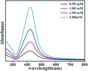
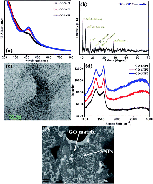
The formation of GO–SNP composite was examined by UV-Vis spectroscopy. Fig. 9a shows the optical absorption spectra of GO–SNP composite for three different levels of SNP dose. The peak occurring at 231 nm, for all the samples, is a characteristic peak for GO due to the π–π* transitions of aromatic C–C bonds.42 The next peak around 300 nm is assigned to the n–π* transition of C![[double bond, length as m-dash]](https://www.rsc.org/images/entities/char_e001.gif) O bonds.2 The slight decrease in absorption intensity with increasing SNP content, for both the peaks ensures removal of more oxygen functional groups i.e. better reduction of GO.43 The attachment of SNPs to the rGO layers is confirmed by the surface plasmon band at 410 nm.44 Higher intensity of absorption at 410 nm with increase in SNP content shows the formation of rGO sheets with greater density of SNPs attached to it.
O bonds.2 The slight decrease in absorption intensity with increasing SNP content, for both the peaks ensures removal of more oxygen functional groups i.e. better reduction of GO.43 The attachment of SNPs to the rGO layers is confirmed by the surface plasmon band at 410 nm.44 Higher intensity of absorption at 410 nm with increase in SNP content shows the formation of rGO sheets with greater density of SNPs attached to it.
 |
| | Fig. 9 (a) UV-Vis absorption spectra of GO–SNP composite with three different SNP loading. (b) XRD profile of a representative nanocomposite sample. (c) TEM image of a representative GO–SNP composite sample. (d) Raman spectrum of GO–SNP composite. (e) SEM image of the channel region of TFT. | |
X-ray diffraction spectra were recorded for the samples to ensure the effectiveness of ex situ approach. Fig. 9b shows the XRD pattern of representative nanocomposite sample. The diffraction peak at 11.05° corresponds to an interlayer spacing of 0.8 nm. This is attributed to the presence of oxygen containing groups into graphene structure.45 In natural graphite, the graphene layers are densely stacked with d-spacing of 0.34 nm.46 After oxidation by Hummer's method, the d-spacing is increased to 0.8 nm because of the incorporation of oxygen groups. The diffraction peaks at 22.2° and 26.2° correspond to d-spacing of 0.4 nm and 0.34 nm respectively which are the signatures of reduction of GO.46,47 Also, the presence of diffraction peak at 17.8° suggests that the GO is reduced to rGO due to UV exposure.48 The characteristic diffraction peak of SNPs occur at 38.2° due to reflections at (111) plane.
Fig. 9c shows the TEM image of a representative nanocomposite sample. The SNPs are nicely decorated on the GO matrix and closely spaced. The size-distribution of SNPs is not disturbed after preparing the composite. The TEM image confirms the ability of GO sheets to anchor the SNPs on their surface. The composite was further characterized by Raman spectroscopy as shown in Fig. 9d. The Raman spectrum for three GO–SNP composites displays two distinct peaks corresponding to D and G bands. The D band peak at 1348 cm−1 is due to disorder or defects in carbon atoms, while the G band at 1598 cm−1 represents the sp2 in-plane vibration of carbon atoms.49 The intensity ratio of the D band and G band (ID/IG) calculated for GO–SNP1, GO–SNP2 and GO–SNP3 is 1.06, 0.99 and 0.94 respectively. The reduction in the ID/IG ratio is due to reduction of GO with increase in SNP loading. In addition, the peak intensities of the D band and G band in composite are significantly increased with increase in SNP loading. This indicates that the surface-enhanced Raman scattering (SERS) activity is due to the intense local electromagnetic fields of the Ag nanoparticles.50 An SEM image of the channel region is shown in Fig. 9e.
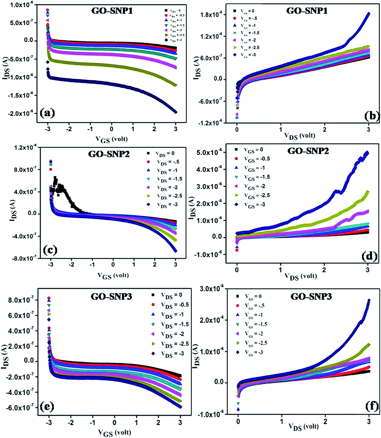
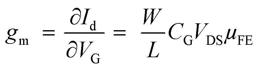
The optical and morphological studies show successful ex situ preparation of nanocomposite. The nanocomposite samples were further used as a channel material in thin film transistor to characterize their field effect properties. The transfer and output characteristics of GO–SNP-TFTs are shown in Fig. 10. The transfer characteristics were obtained by monitoring the drain-source current (IDS) while varying the gate-source voltage (VGS) from −3 V to +3 V with steps of 0.01 V at drain-source (VDS) voltage from 0 V to −3 V with steps of −0.5 V. Similarly, the output characteristics were studied by sweeping the VDS from 0 V to 3 V at VGS from 0 V to −3 V with the same step size. From the output and transfer characteristics it is observed that GO–SNP exhibit p-type charge transport. The field-effect mobility (μFE) of charge carriers was calculated with the given relation, from transfer characteristics,
| |
 | (7) |
where
gm is the transconductance,

is the width-to-length ratio of the channel and
CG is the gate capacitance. From the transfer characteristics the value of
gm is found to be 4.16 × 10
−7 S, 3.55 × 10
−7 S and 1.74 × 10
−7 S respectively for GO–SNP1-TFT, GO–SNP2-TFT and GO–SNP3-TFT taking the value of
CG = 1.15 × 10
−8 F cm
−2 for a 300 nm SiO
2 gate insulator. The current on/off ratio, threshold voltage and subthreshold slope are also calculated from the transfer characteristics.
51,52 The calculated parameters are tabulated in
Table 4.
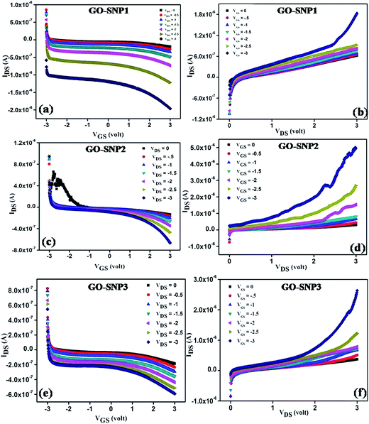 |
| | Fig. 10 The transfer (a) and output (b) characteristics show p-type conduction in GO–SNP1 TFT. The mobility of charge carriers is found to be 2.41 cm2 V−1 s−1. For GO–SNP2 TFT also, the transfer (c) and output (d) characteristics show dominant p-type conduction with mobility 2.06 cm2 V−1 s−1. For GO–SNP3 TFT, the mobility is found to be 1.10 cm2 V−1 s−1. | |
Table 4 Electrical parameters of GO–SNP composite based TFT
| Sample |
Transconductance (gm) (×10−7) S |
Mobility (μFE) (cm2 V−1 s−1) |
Current on/off ratio |
Threshold voltages (V) |
Subthresold slope (V dec−1) |
| GO–SNP1 |
4.16 |
2.41 |
∼102 |
−2.9 |
14.4 |
| GO–SNP2 |
3.55 |
2.06 |
∼102 |
−2.2 |
10.34 |
| GO–SNP3 |
1.84 |
1.10 |
∼102 |
−2.5 |
9.23 |
The transfer and output characteristics of SNP decorated GO TFT exhibits dominant p-type charge transport characteristics. IDS reduces gradually with increase in positive VGS as observed from the transfer characteristics and the p-type charge conduction becomes more prominent as SNP dose increases. Results suggest that the transport behavior of GO can be effectively tuned by decorating with SNPs. The conductivity of the channel reduces with increase in SNP incorporation due to enhanced scattering and defects introduced by SNPs into the layers of GO.53 Similar kind of behavior was observed by Tang et al.54 while studying the electrical properties of boron doped graphene TFT. We have achieved field-effect mobility in the range from 1.10–2.41 cm2 V−1 s−1 depending on the SNP loading and the obtained values are found to be within the range reported earlier.55 It is also observed from the output characteristics that the turn on voltage is getting lowered with increase in SNP loading. The shift in charge neutrality point is attributed to the strong doping effect of oxygen functional groups and impregnated SNPs on GO matrix.56,57
The effect of SNP loading on the transport of charge carriers through the transistor channel was investigated by analyzing the output characteristics of each FET using Fowler–Nordheim (FN) tunneling using the relation
| |
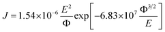 | (8) |
where
J is the field-emission current,
Φ is the work function and
E is the applied electric field.
E can be represented as
E =
βV where
β is denoted as field enhancement factor. The corresponding FN plots (ln(
I/
V2)
vs. (1/
V)) of output characteristics of each transistor is shown in
Fig. 11a–c. The FN plots indicate that the charge transport is carried out by two different mechanisms at two different regimes of applied drain-source voltage.
 |
| | Fig. 11 Fowler–Nordheim plot for (a) GO–SNP1 TFT, (b) GO–SNP2 TFT and (c) GO–SNP3 TFT. (d) Slope of FN plots of each TFT plotted against VGS. | |
In the FN plots, linear characteristic with negative slope is observed at higher applied gate voltages which indicate conduction through FN tunneling. At lower gate voltages, regions with positive slope exhibit multistep hopping of charge carriers. For the three sets of transistors we have observed strong gate dependence of charge transport which in turn varies with SNP loading. For GO–SNP1 TFT, FN tunneling is observed only when VGS = −3 V. For other two TFTs, FN tunneling occurs for VGS = −0.5 to −3 V. To examine the simultaneous effect of gate voltage and SNP loading, slope of the FN regions were extracted and was plotted against VGS as shown in Fig. 11d. The slope of FN plot corresponds to β−1Φ3/2 where Φ is the work function and β is the field enhancement factor defined as the ratio of local surface electric field to applied bias. The value of β depends on device geometry, crystal structure, surface morphology and electrical homogeneity.58 From Fig. 11d, the highest value of FN slope is observed in GO–SNP1 TFT at VGS = −3 V. For GO–SNP2, the slope increases when VGS is changed from −0.5 V to −1 V, and that it varies almost linearly with slight reduction in value. However, in GO–SNP3, the slope reduces slightly when VGS switches from −0.5 V to −1 V and increases linearly thereafter. The dependence of FN slope on VGS validates the effect of gate bias on tunnel barrier height and variation of this dependence for three sets of transistors shows direct relation of field enhancement factor and work function with SNP loading. Since, FN tunneling current is a function of both the field enhancement factor and work function as determined from eqn (2), the individual effect of these two parameters on tunneling current is very difficult to analyze. However, the linear increase in FN slope with negative gate voltage shows dominance of Φ on tunneling current in GO–SNP3 while slight decrease in slope value in GO–SNP2 exhibits the dominance of β on its charge transport. This simply implies the sole performance of SNPs anchored to GO structure in controlling the effect of local electric field. Further studies on this system will provide better control on tuning the transport properties of GO based nanocomposite.
Conclusions
Graphene oxide–silver nanoparticle composite is prepared by a convenient ex situ method with photochemically grown silver nanoparticles. The nucleation of nanoparticles can be triggered with photo excitation. Nucleation time, concentration of precursor, ethanolamine and surfactant are found to control the size and size-distribution of the nanoparticles. The nucleation and growth process is explained by photoinduced electron transfer theory. The ex situ preparation of nanocomposite resulted in successful impregnation of SNPs into GO layers. The composite is used as channel in thin film TFT on Si/SiO2 substrate with Au source and drain contacts in back gated configuration. The TFTs show dominant p-type conduction behavior as a function of SNP concentration. The transport properties of charge carriers can be well controlled by SNP dose. Our study suggests a convenient procedure for synthesis of GO based nanocomposite and also emphasizes the utility of GO–metal nanoparticle composite as a channel material in TFT to have tunable transport properties with existing Si based electronics.
Acknowledgements
One of the authors (KS) acknowledges the financial support from University Grants Commission, Delhi.
References
- G. Eda, C. Mattevi, H. Yamaguchi, H. Kim and M. Chhowalla, J. Phys. Chem. C, 2009, 113, 15768–15771 CAS.
- D. W. Boukhvalov and M. L. Katsnelson, J. Am. Chem. Soc., 2008, 130, 10697–10701 CrossRef CAS PubMed.
- J. I. Paredes, S. Villar-Rodil, A. Martinez-Alonso and J. M. D. Tascon, Langmuir, 2008, 24, 10560–10564 CrossRef CAS PubMed.
- Y. Zhu, S. Murali, W. Cai, X. Li, J. W. Suk, J. R. Potts and R. S. Ruoff, Adv. Mater., 2010, 22, 3906–3924 CrossRef CAS PubMed.
- Y. Zhou, J. Yang, X. Cheng, N. Zhao, H. Sun and D. Li, RSC Adv., 2013, 3, 3391–3398 RSC.
- Y. Shao, H. Wang, Q. Zhang and Y. Li, J. Mater. Chem. C, 2013, 1, 1245–1251 RSC.
- H. K. Jeong, M. H. Jin, K. P. So, S. C. Lim and Y. H. Lee, J. Phys. D: Appl. Phys., 2009, 42, 065418–065424 CrossRef.
- D. A. Dinh, K. S. Hui, K. N. Hui, Y. R. Cho, W. Zhou, X. Hong and H. Chun, Appl. Surf. Sci., 2014, 298, 62–67 CrossRef CAS.
- S. Mandal, R. K. Arun, N. Hanumaiah, N. Chanda, S. Das, P. Agarwal, J. Akhtar and P. R. Mishra, J. Electron. Mater., 2015, 44, 6–12 CrossRef CAS.
- G. Xu, R. Lu, J. Liu, H. Chiu, R. Hui and J. Z. Wu, Adv. Opt. Mater., 2014, 2, 729–736 CrossRef CAS.
- Y. Li, O. Zaluzhna, B. Xu, Y. Gao, J. M. Modest and Y. J. Tong, J. Am. Chem. Soc., 2011, 133, 2092–2097 CrossRef CAS PubMed.
- S. R. K. Perala and S. Kumar, Langmuir, 2013, 29, 9863–9873 CrossRef CAS PubMed.
- V. G. Pol, D. N. Srivastava, O. Palchik, V. Palchik, M. A. Slifkin, A. M. Weiss and A. Gedanken, Langmuir, 2002, 18, 3352–3357 CrossRef CAS.
- J. Yang, H. Yin, J. Jia and Y. Wei, Langmuir, 2011, 27, 5047–5053 CrossRef CAS PubMed.
- B. Hu, S. B. Wang, K. Wang, M. Zhang and S. H. Yu, J. Phys. Chem. C, 2008, 112, 11169–11174 CAS.
- A. R. Shahverdi, S. Minaeian, H. R. Shahverdi, H. Jamalifar and A. A. Nohi, Process Biochem., 2007, 42, 919–926 CrossRef CAS.
- F. Mafune, J. Kohno, Y. Takeda and T. Kondow, J. Phys. Chem. B, 2000, 104, 9111–9117 CrossRef CAS.
- Y. H. Chen and C. S. Yeh, Colloids Surf., A, 2002, 197, 133–139 CrossRef CAS.
- L. M. Huang, W. H. Liao, H. C. Ling and T. C. Wen, Mater. Chem. Phys., 2009, 116, 474–478 CrossRef CAS.
- J. Yang, E. Sargent, S. Kelley and J. Y. Ying, Nat. Mater., 2009, 8, 683–689 CrossRef CAS PubMed.
- W. Zhang, X. Qiao and J. Chen, J. Mater. Sci. Eng. B, 2007, 142, 1–15 CrossRef CAS.
- E. C. Njagi, H. Huang, L. Stafford, H. Genuino, H. M. Galindo, J. B. Collins, G. E. Hoag and S. L. Suib, Langmuir, 2011, 27, 264–271 CrossRef CAS PubMed.
- B. Yin, H. Ma, S. Wang and S. Chen, J. Phys. Chem. B, 2003, 107, 8898–8904 CrossRef CAS.
- B. Yang, Z. Liu, Z. Guo, W. Zhang, M. Wan, X. Qin and H. Zhong, Appl. Surf. Sci., 2014, 316, 22–27 CrossRef CAS.
- M. Sakamoto, M. Fujistuka and T. Majima, J. Photochem. Photobiol., C, 2009, 10, 33–56 CrossRef CAS.
- S. Jradi, L. Balan, X. H. Zeng, J. Plain, D. J. Lougnot, P. Royer, R. Bachelot, S. Akil, O. Soppera and L. Vidal, Nanotechnology, 2010, 21, 095605–095612 CrossRef CAS PubMed.
- P. K. Sudeep and P. V. Kamat, Chem. Mater., 2005, 17, 5404–5410 CrossRef CAS.
- F. Mafune, J. Kohno, Y. Takeda, T. Kondow and H. Sawabe, J. Phys. Chem. B, 2000, 104, 9111–9117 CrossRef CAS.
- H. Hada, Y. Yonezawa, A. Yoshida and A. Kurakake, J. Phys. Chem., 1976, 80, 2728–2731 CrossRef CAS.
- A. Panacek, L. Kvitek, R. Prucek, M. Kolar, R. Vecerova, N. Pizurova, V. K. Sharma, T. Nevecna and R. Zboril, J. Phys. Chem. B, 2006, 110, 16248–16253 CrossRef CAS PubMed.
- B. Hu, S. B. Wang, K. Wang, M. Zhang and S. H. Yu, J. Phys. Chem. C, 2008, 112, 11169–11174 CAS.
- M. Yamamoto, Y. Kashiwagi and M. Nakamoto, Langmuir, 2006, 22, 8581–8586 CrossRef CAS PubMed.
- X. Dong, X. Ji, H. Wu, L. Zhao, J. Li and W. Yang, J. Phys. Chem. C, 2009, 113, 6573–6576 CAS.
- B. Pietrobon and V. Kitaev, Chem. Mater., 2008, 20, 5186–5190 CrossRef CAS.
- S. K. Mehta, S. Chaudhary and M. Gradzielski, J. Colloid Interface Sci., 2010, 343, 447–453 CrossRef CAS PubMed.
- F. Wang, V. N. Richards, S. P. Shields and W. E. Buhro, Chem. Mater., 2014, 26, 5–21 CrossRef CAS.
- D. Jose, J. E. Matthiesen, C. Parsons, C. M. Sorensen and K. J. Klabunde, J. Phys. Chem. Lett., 2012, 3, 885–890 CrossRef CAS PubMed.
- D. S. Sidhaye and B. L. V. Prasad, New J. Chem., 2011, 35, 755–763 Search PubMed.
- H. M. Zheng, R. K. Smith, Y. W. Jun, C. Kisielowski, U. Dahmen and A. P. Alivisatos, Science, 2009, 324(5932), 1309–1312 CrossRef CAS PubMed.
- Y. Liu, K. Tai and S. Dillon, Chem. Mater., 2013, 25, 2927–2933 CrossRef CAS.
- S. P. Shields, V. N. Richards and W. E. Buhro, Chem. Mater., 2010, 22, 3212–3225 CrossRef CAS.
- J. Li and C. Y. Liu, Eur. J. Inorg. Chem., 2010, 1244–1248 CrossRef CAS.
- V. H. Pham, T. V. Cuong, S. H. Hur, E. W. Shin, J. S. Kim, J. S. Chung and E. J. Kim, Carbon, 2010, 48, 1945–1951 CrossRef CAS.
- M. R. Das, R. K. Sarma, R. Saikia, V. S. Kale, M. V. Shelke and P. Sengupta, Colloids Surf., B, 2011, 83, 16–22 CrossRef CAS PubMed.
- D. R. Dreyer, S. Park, C. W. Bielawski and R. S. Ruoff, Chem. Soc. Rev., 2010, 39, 228–240 RSC.
- Y. Qian, A. Vu, W. Smyrl and A. Stein, J. Electrochem. Soc., 2012, 159, A1135–A1140 CrossRef CAS.
- H. P. Cong, X. C. Ren, P. Wang and S. H. Yu, Sci. Rep., 2012, 2, 1–6 Search PubMed.
- M. Zainy, N. M. Huang, S. V. Kumar, C. H. Chia and I. Harrison, Mater. Lett., 2012, 89, 180–183 CrossRef CAS.
- J. Shen, T. Li, Y. Long, M. Shi, N. Li and M. Ye, Carbon, 2012, 50, 2134–2174 CrossRef CAS.
- J. Li and C. Liu, Eur. J. Inorg. Chem., 2010, 1244–1252 CrossRef CAS.
- W. Xu and S. W. Rhee, Org. Electron., 2011, 12, 2040–2046 CrossRef CAS.
- W. Xu, C. Guo and S. W. Rhee, J. Mater. Chem. C, 2013, 1, 3955–3960 RSC.
- B. D. Guo, Q. Liu, E. D. Chen, H. W. Zhu, L. Fang and J. R. Gong, Nano Lett., 2010, 10, 4975–4980 CrossRef CAS PubMed.
- Y. B. Tang, L. C. Yin, Y. Yang, X. H. Bo, Y. L. Cao, H. E. Wang, W. J. Zhang, I. Bello, S. T. Lee, H. M. Cheng and C. S. Lee, ACS Nano, 2012, 6, 1970–1978 CrossRef CAS PubMed.
- C. Gomez-Navarro, R. T. Weitz, A. M. Bittner, M. Scolari, A. Mews, M. Burghard and K. Kern, Nano Lett., 2007, 7, 3499–3503 CrossRef CAS PubMed.
- W. Xu, L. Wang, Y. Liu, S. Thomas, H. K. Seo, K. I. Kim, K. S. Kim and T. W. Lee, Adv. Mater., 2015, 27, 1619–1623 CrossRef CAS PubMed.
- W. Xu, T. S. Lim, H. K. Seo, S. Y. Min, H. Cho, M. H. Park, Y. H. Kim and T. W. Lee, Small, 2014, 10, 1999–2005 CrossRef CAS PubMed.
- F. Cicoira and C. Santato, Adv. Funct. Mater., 2007, 17, 3421–3434 CrossRef CAS.
|
| This journal is © The Royal Society of Chemistry 2015 |
Click here to see how this site uses Cookies. View our privacy policy here. 


 .
.
 in eqn (4) simply gives us the rate at which concentration of solute is reducing. In photoinduced electron transfer reactions this rate is simply equal to the rate of electron transfer (αel). Therefore, we arrive at the expression,


 is the width-to-length ratio of the channel and CG is the gate capacitance. From the transfer characteristics the value of gm is found to be 4.16 × 10⁻⁷ S, 3.55 × 10⁻⁷ S and 1.74 × 10⁻⁷ S respectively for GO–SNP1-TFT, GO–SNP2-TFT and GO–SNP3-TFT taking the value of CG = 1.15 × 10⁻⁸ F cm−2 for a 300 nm SiO2 gate insulator. The current on/off ratio, threshold voltage and subthreshold slope are also calculated from the transfer characteristics.51,52 The calculated parameters are tabulated in Table 4.