Thermoplastic building blocks for the fabrication of microfluidic masters

Michael A. Stollera, Abhiteja Kondaa, Matthew A. Kottwitza and Stephen A. Morin*ab
aDepartment of Chemistry, University of Nebraska–Lincoln, Lincoln, NE 68588, USA. E-mail: smorin2@unl.edu
bNebraska Center for Materials and Nanoscience, University of Nebraska–Lincoln, Lincoln, NE 68588, USA

Received 29th October 2015 , Accepted 10th November 2015

First published on 12th November 2015


Abstract

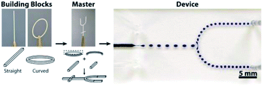
Microfluidic channels are typically fabricated in polydimethylsiloxane (PDMS) using a combination of photolithography and soft lithography. Photolithography, while ubiquitous in the fabrication of microfluidic devices, generally requires skilled technicians, expensive chemicals, and specialized equipment. This manuscript describes a simple method for the fabrication of masters for use in soft lithography that is based on combining thermoplastic “building blocks” using thermal “welding.” This approach is applicable to the fabrication of an array of devices that possess many of the basic functionalities (e.g., droplet generation, mixing, and splitting) required in microfluidics. In addition to these systems, which are routinely fabricated using photolithographically produced masters, this manuscript describes how thermoplastic building blocks can be stacked, assembled, and replicated to fabricate microfluidic devices with channel crossings and/or channels of variable cross-sectional height—geometries that normally require multiple steps of photolithography. The methods described here enable a range of scientists of varying expertise to prototype a variety of functional microfluidic devices easily and rapidly, even when access to traditional fabrication techniques or time is limited, or when an optimized design is not available.


Introduction

Functional microfluidic devices are composed of networks of micron-scale channels.1 The masters used in the soft lithographic fabrication of microfluidic devices are generally produced via photolithography, which requires photomasks, skilled technicians, expensive chemicals, and specialized equipment.2–5 The requirements of photolithography can restrict the throughput and increase the cost of producing masters, thus limiting the use of this method of fabrication in certain applications (i.e., ones that require rapid iterations of designs) and settings (i.e., when photolithographic equipment is unavailable). We desired a method that was capable of prototyping masters for two-dimensional (2D) microfluidic devices that does not require specialized equipment, lengthy procedures, or toxic and expensive chemicals. Ideally this method would be: (i) applicable to the fabrication of functional components that are common to microfluidics (i.e., passive mixers, droplet generators, etc.), (ii) capable of producing large-area/multifunctional networks of micro-channels, and (iii) adaptable to laboratories with a range of technical capabilities.

Our strategy was to fabricate a standardized set of building blocks (straight and curved units with rectangular cross-sections of micron-scale dimensions) from thermoplastics that we could then assemble into the desired masters. The process of assembly, used a combination of cutting and placing and thermal processing to modify and fuse the blocks into continuous structures. We used three-dimensional (3D) printing to prototype the building blocks; however, other manufacturing techniques (e.g., injection or extrusion molding) can also produce the blocks we report. Once fabricated, these masters (which could consist of many blocks, or single, directly printed blocks) were suitable for generating microfluidic devices via soft lithography (Fig. 1). Although the building blocks used had set cross-sectional dimensions, we stacked the blocks and joined them using thermal processing to generate unique segments with variable cross-sectional dimensions that enabled the production of microfluidic systems with channels of varying height. These devices would be difficult to produce using single-step photolithography. We also developed methods for the reversible assembly of the thermoplastic building blocks, enabling reconfiguration of the blocks.


image file: c5ra22742a-f1.tif
Fig. 1 Device fabrication using 3D-printed ABS masters. (A) Schematic illustration of the fabrication of a microfluidic device using a thermoplastic master of rectangular cross-section and soft lithography: (i) the master is placed on a glass substrate, (ii) covered with PDMS pre-polymer, (iii) cured and the stamp demolded from the glass/master, and (iv) bonded to glass and finished with inlet/outlet tubes. (B–E) Photographs of the masters used to fabricate the corresponding microfluidic devices shown in the right column: (F) a straight channel, (G) a rectilinear channel network, (H) a spiral channel, and (I) a serpentine channel.

Using a limited “set” of standardized building blocks we fabricated the masters required to produce a range of 2D and 3D microfluidic devices with useful fluidic functionality. This approach provides, in one toolset, routes to devices with bridges and multi-level networks6,7 using simple tools, like ovens, glass plates, and razor blades, that are available in virtually any laboratory, makers space, or teaching facility. This approach will be useful to those wishing to prototype microfluidic devices rapidly, but that do not have the specialized equipment or time required for photolithography, or to those who wish to explore microfluidics, but lack the resources to out-source the process of master fabrication to third parties. Our approach is applicable to large-area devices and channels of varying heights without requiring a new set of building blocks.

The micron-scale channels in microfluidic devices provide low-volume flow at low Reynolds numbers, and thus fluidic functions that are not possible in larger channels.8 By controlling the geometry of the networks of channels in microfluidic devices many useful capabilities (e.g., the combination, mixing, and/or division of flow) may be accessed. Some of the most common and useful components that enable such functions include: junctions, mixers, droplet generators and sorters, and optical analysis zones.9,10 Junctions allow flow from two or more channels to be combined into one channel. When a “Y” junction is used, low Reynolds numbers give laminar flow and the two solutions flow through a single channel with minimal mixing. Passive mixing of laminar flows is achieved using micro-channels with, for example, herringbone,11 serpentine,12 and/or circular geometries.13 In droplet-based microfluidic systems, two immiscible fluids are used to create discrete volumes of a single phase (gas or liquid) dispersed in another phase.14,15 Droplets are typically formed using “flow-focusing” or “T” junction micro-channel geometries.16–18 Droplet generators may be combined with fluidic mixers to homogenize the liquid/solution inside individual droplets.19 Each discrete droplet can act as its own micro-reactor, allowing for high throughput reactions at high rates of speed.20,21

Early on, microfluidic devices were fabricated almost exclusively from silicon and glass following established photolithographic techniques.22–24 Soft lithography with photolithographically produced masters is now the preferred method of microfluidic device fabrication in research labs because it is fast, simple, and does not require the use of expensive chemicals (once the master is produced), thereby making it the ideal technique for prototyping.5 We take advantage of these characteristics of soft lithography in the current work, focusing on simplifying master fabrication.

Despite the diversity of functionalities and methods of fabrication in microfluidics, there remains a gap between the makers of microfluidic devices and the range of users that may benefit from these devices. In some cases, the researchers who want to use microfluidic devices do not have the resources (e.g., clean room facilities) or skills required to produce such devices themselves using traditional means. In order to address this gap several groups have developed systems of modular microfluidics (micro-assembly blocks, interlocking connectors, bread board microfluidics, etc.) as alternatives to traditional microfluidic fabrication.25–32 These systems consist of single function fluidic devices with interconnects that allow for their rapid combination and reconfiguration into unique microfluidic devices.29 Others have used flexible ABS filaments as sacrificial interconnects to join photolithographically produced masters; this approach allowed for easy reconfiguration of devices and minimized the length of channel between functional components.6

Modular microfluidics generally follows the methods of photolithography and soft lithography in fabrication. Other techniques such as micromachining, stereolithography, injection molding, and embossing are being explored for the rapid fabrication of microfluidic devices.33–36 In addition to these techniques, 3D-printing has grown quickly as a method for the fabrication of microfluidic devices.37 Using 3D-printing, it is possible to fabricate a functional fluidic system directly from a computer-designed prototype,38,39 or the masters required to produce such devices using soft lithography.37 There are also examples where 3D channel networks have been fabricated in PDMS using 3D printed structures.7 Previously, we have prototyped and fabricated a variety of microfluidic devices using 3D-printed masters.40 3D-printing offers unique advantages over traditional fabrication methods: toxic chemicals are not required, large-area devices can be accessed more easily and cost effectively, and rapid prototyping is simplified by avoiding photolithography. Despite the numerous advantages, masters made by 3D-printing are produced with less precision than those produced by photolithography and the process can still be time consuming (build times are on the order of hours depending on the printer). In 3D-printing, solid objects are produced by stacking several 2D layers on top of each other. This layer-by-layer manufacturing leads to surface defects in the part and slows production times. Recent advancements in the area of “layerless” 3D-printing promise to shorten manufacturing times, and increase the fidelity of the final product;41 however, the vast majority of 3D-printed parts and printers still have the limitations of layer-by-layer fabrication.

Experimental design

Masters from building blocks

We modularize the process of master fabrication using thermoplastic building blocks thus enabling researchers with a wide range of skills to fabricate functional microfluidic devices, and suggest that this approach will provide greater flexibility, in some cases, than modular fluidics or 3D-printed devices (Fig. 2). Users of the current modular microfluidic systems are limited by the set of components available; however, by using building blocks to fabricate customized masters, nearly any 2D network of channels can be designed and produced. Fabrication that is based on 3D-printing remains limited by the resolution and the range of build materials that are readily available using commercial printing systems. Further, even when the printers and applicable materials are available, fabrication of pre-made parts is faster.
image file: c5ra22742a-f2.tif
Fig. 2 Device fabrication using building blocks. (A and B) Technical drawings of the standardized building blocks used in fabrication of the masters, and (C) representative photographs of the building blocks. (D) Schematic illustrating master fabrication via thermal welding: (i) building blocks are placed on glass, (ii) arranged, (iii) covered with a second piece of glass, and (iv) heated to thermally weld the blocks into functional masters of the desired geometry. (E, H and K) Schematic illustrating the set of building blocks that were used to create various masters, (F, I and L) the corresponding photographs of the assembled masters, and (G, J and M) the fabricated microfluidic devices. All scale bars are 5 mm.

We chose to fabricate the building blocks from acrylonitrile butadiene styrene (ABS) because it has a relatively low glass transition temperature that is convenient for thermal processing (e.g., joining via thermal “welding,” Fig. 2D), and because ABS is widely used in 3D-printing and manufacturing in general.42 The low glass transition temperature of ABS is still high enough that the blocks remained stable at the temperatures necessary for thermal curing of PDMS. For prototyping the building blocks using 3D-printing, we limited the volume of the print jobs to that of the channels to minimize print time, and processed the as-printed blocks using thermal annealing against glass to remove defects on the surface of the blocks. We thus retained the advantages of 3D-printing in prototyping, while minimizing some of the disadvantages.

The manual alignment and assembly of micron-scale building blocks could seem cumbersome, irreproducible, and time consuming. To the contrary, we found that electrostatic interactions between the thermoplastic blocks and the glass substrates used: (i) led to an attraction between the building blocks and the substrate that resisted lateral movement and thus minimized the dexterity necessary to position blocks by hand, and enabled precise and reproducible placement of blocks, and (ii) brought the building blocks into conformal contact with the underlying glass support, preventing pre-polymer from seeping between the master and the support substrate during soft lithographic replication (Fig. 1A). This tendency for the blocks to “stick” to glass during assembly was a result of the position of ABS in the triboseries relative to glass.43

Thermal assembly of blocks

We used heat to “weld” (when irreversible bonding was required) the ABS building blocks together because it is experimentally convenient and ovens capable of reaching temperatures above the glass transition of ABS are found in most laboratories (Fig. 2D). Additionally, thermal annealing against glass (“pressing”) allows the cross-sectional dimensions of thermoplastic masters to be easily tuned, in addition to smoothing out the imperfections associated with extrusion based 3D-printing (see ESI text, Fig. S1). Together, thermal pressing and welding of thermoplastic building blocks provides a simple method to reproducibly generate structures of the required geometry for the fabrication of functional microfluidic components. Photolithography or direct printing of masters cannot rapidly, and with the same level of processing flexibility, access the range of geometries offered by this approach. Once assembled, the masters were directly applicable to soft lithography.

Functional systems by lateral combination and stacking of blocks

In order to demonstrate the applicability of thermally assembled building blocks to the fabrication of microfluidic systems with the critical functions required, we focused our demonstrations on the following components: passive mixers, droplet generators, droplet sorters, and droplet mixers.44 Combining these simple components into masters of designs that have the desired geometry/order of functionality enable the fabrication of microfluidic systems with functional characteristics suited for a particular application (e.g., encapsulating reagents in droplets for mixing and parsing). In these demonstrations only lateral organization of the blocks was required.

By combining lateral assembly with stacking, we expanded the potential geometries accessible using a limited set of building blocks to include those of varying cross-sectional height. Variable height channels are applicable to the field of optofluidics, which concerns the optical detection of analytes flowing within micron-scale channels.9,10 The small cross-sectional dimensions of micro-channels limits their optical path length, and thus the sensitivity attainable using optical absorption and fluorescence measurements.34 Microfluidic systems with varying aspect/high aspect ratio channels have been explored in optofluidics as a potential solution to the limitations of absorbance measurements.45 Furthermore, systems with channels of varying cross-sectional heights have been applied in the localization of cells inside microchambers, the creation of uniform microenvironments for cell growth, high throughput cell screening, and bubble generation/transport.44,46,47 Stacking blocks circumvents the need for multistep photolithography to fabricate micro-channels with varying heights, simplifying fabrication of devices for these applications.

We combined the utility of stacking with “bridging” to enable the design and fabrication of multi-level channel networks.6,7 This approach (because the blocks are regular and stacked/assembled in a rectilinear fashion along z) simplified control of the vertical distance between channels in the fabrication of multi-level networks. Further, by using “sacrificial” welds at the bridging sites, we could demold the structures without tearing the PDMS stamp (as was not the case in solid 3D masters7) (see ESI text). This procedure did not require the use of solvents (which could introduce contaminants) mainly because the blocks were smooth (from heat treatment) and the lengths of the bridges could be minimized in design. This approach can complement methods based on 3D printing, and provide a convenient alternative (in terms of technical requirements and/or time) to direct internal 3D laser writing methods, and methods based on stacking layers with registered through-holes.48,49

Results & discussion

Building block design

We used a 3D-printer to directly fabricate ABS masters that consisted of thin rectangular cross-sections (a range of cross-sectional dimensions, height × width, of 250–1000 μm × 450–1000 μm, were investigated) of the desired network design. The 3D-printer we used was capable of printing blocks with cross sectional dimension down to 270 ± 10 μm × 440 ± 60 μm (Fig. S1). This cross sectional dimension approaches the smallest that would be feasible to assemble by hand, especially for complicated channel geometries. If a higher resolution printer was used, smaller master dimensions could be accessed at the cost of ease of assembly. The (practical) feature resolution (i.e., the separation between parallel channels) we could achieve was 250 μm. Again, this parameter could be improved using higher resolution printing.

We did not print the entire device or the channel design with a “base” attached, rather, we only printed the channel segments themselves, minimizing print volumes, and allowing for investigation of 3D-printed ABS “strips” to microfluidic fabrication. Using this approach, we rapidly produced (at 35 seconds per 1 cm of channel length) many masters with unique channel designs of varying size and complexity, and then used them to fabricate functional devices via soft lithography (Fig. 1). These devices were simple one inlet/outlet devices that provided evidence of the applicability of the blocks to a slightly adapted approach to soft lithographic replication where the master was supported on glass and covered with PDMS pre-polymer (Fig. 1A). We did not have any issues sealing these replicates following standard plasma bonding protocols or introducing inlets/outlets using biopsy punches.50 We note that when plasma bonding is unavailable, compression or van der Walls interactions can be used to seal the devices.40,50

We used these investigations to establish the limitations, especially in terms of channel dimensions, geometry, and the durability of the master, of 3D-printed building blocks important to the design of a standardized set of blocks for subsequent demonstrations. We determined that rectangular segments with cross-sectional dimensions of 300 μm × 450 μm (where these dimensions are those sent to the printer and 270 ± 10 μm × 440 ± 60 μm are the actual as-printed dimensions measured with profilometry, Fig. S1) were most reliable in fabrication and practical in manual manipulation. Other dimensions also worked, but for the purposes of the remaining demonstrations, we used these dimensions as the basis for the 3D-printed building blocks. We produced a set of blocks consisting of straight, rectangular segments and curved segments of varying radii (Fig. 2A–C).

Assembly of blocks for master fabrication

We cut and assembled the building blocks into masters of various geometries that were applicable to the fabrication of simple one inlet/outlet microfluidic devices (Fig. 2D–M) similar to those directly printed. In these demonstrations we used a grid—simple graph paper with various geometries, such as a 1 mm × 1 mm square pattern—to guide the placement of the blocks on the glass substrate (where the grid was under the glass). We also demonstrated the utility of stencils in the templated fabrication of multiple, identical masters—a strategy that increased the reproducibility of placement of the blocks (see ESI text, Fig. S2).

We used designs with right angles or head-to-head block arrangement to test the mechanical stability of thermally welded pieces during manipulation and replication (these configurations have the minimal contact area between two blocks and represent the weakest weld). We measured this stability using a materials testing system (see ESI text, Fig. S4), and found head-to-head welds fractured at 0.10 ± 0.01 N of tensile force while the solid blocks required 4.6 ± 0.2 N of tensile force. These measurements reveal the weakness of the weld relative to the blocks themselves (∼95% less load is required to break the weld); nevertheless, the bond formed through thermal welding is strong enough to support the manipulation and replication required for device fabrication. The average roughness of the blocks after thermal pressing/welding was ±3.6 μm (with a range from ±9.7 μm to ±0.3 μm) and there was not a significant difference between the body of the block and the weld site (Fig. S5). Further, we measured the fluctuations in the width of the welded masters by analysing three separate 3.5 mm segments of channel that each included one weld site and found the average fluctuation to be ±20 μm (Fig. S5). Using the assembly of building blocks, we could generate a range of 2D channel geometries rapidly. A master that includes ten blocks (nine welds), can be designed and prepared in less than an hour.

The time used for the thermal pressing/welding of the ABS blocks, was important to the final dimensions of the masters (and thus the micro-channels in the devices), and we observed that under the standard thermal processing conditions used in welding, the final cross-sectional dimensions of the masters were 200 ± 20 μm × 670 ± 90 μm (Fig. S1C). In a similar analysis, we determined the dimensions and cross-sectional geometry of the masters at the weld sites (Fig. S5). For the three unique weld geometries (head-to-head and “T” configurations involving straight-curved or straight–straight junctions) investigated, the dimensions of the weld were the same (within error) as that of the solid block. It is possible to exploit thermal pressing to access a range of channel dimensions from the same standard block (Fig. S1C), but here, we have focused on a constant set of conditions for welding the blocks (see ESI text). In some cases the changes in dimensions associated with welding may not be wanted, and we were able to cast devices from blocks that were not permanently fused. This approach meant that the dimensions did not change and that the blocks could be recycled many times—a capability we found extremely useful for reversibly assembling masters (see ESI text).

Functional fluidic components

With the techniques required to fabricate simple, one inlet/outlet devices using building blocks in place, we then used this method to generate more challenging masters for use in the fabrication of functional fluidic components. These functional components, made from combinations of the same standard set of building blocks (Fig. 2A–C), included: a “Y” junction (Fig. 3A, F and K), a “T” junction droplet generator (Fig. 3B, G and L), a flow-focusing droplet generator (Fig. 3C, H and M), a droplet splitter (Fig. 3D, I and N), and a variable cross-section micro-channel (Fig. 3E, J and O). To test the ability of these devices to perform the intended functions, we pumped combinations of colored aqueous solutions and/or oil through the devices. In each example, the functionality was comparable to devices that were fabricated using traditional techniques (e.g., photolithography and soft lithography): the “Y” junction supported laminar flow (Fig. 3K), the microfluidic droplet generators successfully formed water in oil emulsions (Fig. 3L and M, Videos S1 and S2), and the droplet splitter divided individual droplets (Fig. 3N, Video S3).
image file: c5ra22742a-f3.tif
Fig. 3 Fabrication of functional fluidic components using building blocks. (A–E) Schematic illustrations of standard thermoplastic building blocks that were cut into subdivisions and combined to form the masters used to fabricate the corresponding microfluidic devices. (F–J) Photographs of the assembled masters. (K–O) Photographs of the functional microfluidic devices as colored aqueous solutions and/or oil were flowed through them: (K) a “Y” junction, (L) a “T” junction droplet generator, (M) a flow focusing droplet generator, (N) a droplet splitter, and (O) a variable height microfluidic device. All scale bars are 5 mm and inlets/channels flowing oil are annotated with circles and dashed lines.

We acknowledge that these devices are not without defects—particularly at the edges of the channels and at the welding sites (Fig. S6, videos S5–S8)—but observed that these defects did not interrupt the desired function. For example, we analyzed the monodispersity of the droplets formed in “T” junction (Fig. 3L and S7A–C), and flow-focusing droplet generators (Fig. 3M and S7D–F) and found the volumes to be 114 ± 9 nL and 140 ± 7 nL respectively (n = 50, see ESI text). The droplet populations were relatively monodisperse, with a coefficient of variation in volume of <5% for droplets generated by flow-focusing, and <8% for droplets generated by a “T” junction; these coefficients are comparable to what others have achieved using photolithographically produced devices.51,52 Following the split, droplets maintained a coefficient of variation in volume of <5%.

We did minimize defects in the devices by standardizing the welding procedure used to join the thermoplastic building blocks, and by carefully demolding the devices. Occasionally, large defects caused partial or full blockage of the channel, or the generation of satellite droplets (Fig. S4D). The general procedure we have described has a success rate close to 100%—for the fabrication of ten masters/devices, we could routinely produce nine functional devices. Further, fabrication of these devices, including time for design, was less than three hours, with more than half of that time being devoted to preparing and curing PDMS.

Optical absorption in variable cross-section devices

We produced variable height channels by stacking building blocks and thermally welding them (Fig. 3E, J and O and 4). In a typical device the channel consisted of sections of 420 ± 10 μm in height connected by sections of 200 ± 10 μm in height (the width remained constant). As fluid transferred between the sections, there was a corresponding change in velocity (high velocity in the sections with the standard height; relatively low velocity in the taller sections). We illustrated this behavior by passing droplets through a device (Fig. 3O, Video S8).
image file: c5ra22742a-f4.tif
Fig. 4 Optical absorption in variable height channels. (A) A standard building block and (B) a stack of two building blocks used to fabricate devices with constant or variable height channels respectively. (C and D) Top-down and (E and F) edge-on view photographs of a (C and E) constant height and a (D and F) variable height device with indigo carmine flowing through the channels. (G) Absorbance calibration curves collected using a device with a standard height channel and a variable height (stacked) channel. The location of the incident light (I0) is noted in panels (A and B). All scale bars are 5 mm.

Microfluidic devices with channels of variable height can be used to include optical absorption “zones” that increase the signal in UV-visible absorption spectroscopy of the contents of the micro-channels. Beer's law, A = εbc, where A is absorbance, ε is molar absorptivity, b is path length of the absorbing medium, and c is concentration of the analyte, expresses the proportionality between absorbance and path length—by increasing the path length of the light absorbing medium while holding analyte concentration constant, the absorbance can be increased. To demonstrate this ability we measured the absorbance of a set of standard solutions containing indigo carmine dye in two micro-channels: one made from a standard building block (Fig. 4A, C and E) and the other made by stacking two blocks (Fig. 4B, D and F). The difference in height in these devices was apparent using top down and edge-on photography (Fig. 4C–F).

In this study, we observed a more intense absorption signal for the device fabricated with stacked blocks (which gives a taller channel), as illustrated by the calibration curves constructed using each geometry (Fig. 4G). From these calibration curves we determined the limit of detection (S/N = 3) and limit of quantification (S/N = 10) of the indigo carmine dye in the standard height channel to be 1.90 × 10⁻⁵ M and 6.33 × 10⁻⁵ M respectively, versus 8.27 × 10⁻⁶ M and 2.76 × 10⁻⁵ M, respectively, in the taller channel. The limit of detection in the taller channel was an order of magnitude lower than the limit of detection in the standard channel; the limit of quantification in the taller channel was 70% lower than that of the standard channel. This demonstration agrees with the behavior predicted by Beer's law: when ε and c are constant the slope of the calibration line should increase proportionally with b. In this case b was increased by a factor of two (as measured using optical microscopy the standard channel was 200 ± 10 μm and the taller channel was 420 ± 10 μm) and we expected a factor of two difference in the slope. Indeed, we measured the slope of the standard height channel to be 280 ± 20 M−1 and the slope of the taller channel to be 640 ± 20 M−1; a difference of roughly a factor of two. By stacking building blocks, we have demonstrated that we can easily fabricate microfluidic devices with segments of increased height that have utility in optofluidics, such as on-device absorption measurements.

Microfluidic system from functional fluidic components

To elaborate this approach into a hierarchical methodology for fabricating microfluidic systems of increased sophistication, we used building blocks to fabricate functional components and then combined those components into microfluidic systems. For these demonstrations we took advantage of reversible assembly, as this approach minimized the need to remake the masters for each device (see ESI text). The area of devices fabricated using photolithography is limited by the size of the silicon wafer, where typical silicon wafers sizes range from 2–12 inches in diameter, and the size of the area of UV exposure used. Using our methods of fabrication, as demonstrated in these systems, the only limitation on the area of the device made was the size of the glass substrate (see ESI text). We could have demonstrated these devices in a smaller footprint, but intentionally used large-area layouts to illustrate the channel components and the ability to push towards larger devices.

We focus on two systems: the first system combined the functions of a “Y” junction, a “T” junction droplet generator, and a variable height channel to form and mix the contents of droplets containing two aqueous phases (Fig. 5, Video S9); the second system combined a “Y” junction, two passive mixing zones, and a absorption zone formed by a section of taller channel to perform on-device colorimetric measurements of iron in aqueous solutions (Fig. 6). In the first system, we observed enhanced mixing of two aqueous dyes (blue and yellow which gave green when mixed) within droplets that flowed through a device with a variable height channel (Fig. 5A–C and G), compared to a device with a constant channel height (Fig. 5D–F and H). We constructed grayscale intensity profiles across two droplets exiting the devices to illustrate (qualitatively) the different degree of mixing within droplets flowed through a variable height channel (Fig. 5G) and a constant height channel (Fig. 5H). Devices that incorporate variable height segments could be useful in minimizing the length of channel needed to mix reagents in droplets. Such variable height “mixing zones” could also be applied to mixing continuous flows, thus minimizing the lateral footprint of these devices.


image file: c5ra22742a-f5.tif
Fig. 5 Fabrication of a microfluidic system with multiple functional components. (A and D) Schematic illustrations of the components (“Y” junction, “T” junction, and a variable height segment, or a constant height segment) that were combined to form two microfluidic systems. (B and E) Color-coded layout of the systems, with a legend indicating inlets/outlets. (C and F) Photographs of the microfluidic systems in operation. The segments noted i., ii., and iii. are shown at higher magnification in the panels below. (C-i. and F-i.) A “Y” junction feeds two reagents into a flow-focusing droplet generator producing bi-colored janus droplets, (C-ii. and iii.) the droplets containing the two reagents flow into a variable height channel, which drives mixing within each droplet as indicated by the color change (blue/yellow to green), or (F-ii. and iii.) into a constant height channel where mixing was less effective. (G and H) Grayscale intensity profiles which indicate the degree of mixing of colored aqueous dyes within droplets that flowed through (G) a variable height channel and (H) a constant height channel. The profiles were generated along the bisecting lines indicated on the inset images (scale bars are 500 μm) of the droplets analysed (which are marked with a dashed box in panels (C and F)).

image file: c5ra22742a-f6.tif
Fig. 6 On-device colorimetric determination of iron. (A) Schematic illustration of the channel geometry, and (B) photograph of the device as yellow and blue dyes are flowed through it. (C) Plot of intensity measured at the absorption zone in panel A as three Fe samples and standard Fe solutions are passed through the device. Each dip in intensity corresponds to a different iron sample (standard or unknown). (D) Quantification of iron weight percentage in three solid samples on-device, in-flow, or using a cuvette and benchtop spectrometer; 98% confidence intervals are shown. Samples 1, 2, and 3 had known weight percentage of 2.14%, 3.53%, and 3.88% respectively.

The second system illustrates on-device colorimetric quantification/detection of iron.53 Standard iron solutions and three samples of iron (prepared by dissolving/diluting solid samples with known weight percentages of iron) were flowed through the device and mixed with a complexing agent (1,10-phenanthroline) in two mixing zones, yielding a red complex (ferroin). The absorbance of ferroin was monitored through a segment of channel with twice the height of the standard channel as the various solutions were flowed through the device (Fig. 6A–C). We note that for visualization of the device geometry, colored aqueous dyes were used (Fig. 6B). The absorbance signal collected was used to construct a calibration curve (Fig. S6), and quantify the iron percentages of the three samples. The accuracy of our on-device, in-flow absorption measurements was compared to a traditional UV-vis absorption experiment run in parallel using cuvettes and a bench-top spectrometer and, at 98% confidence, the measurements were not different (Fig. 6D). The percent absolute error was 2% using the traditional UV-vis absorption experiment versus 4% using our device. The majority of the error, which is apparent as periodic oscillation in the in-flow absorption signal (Fig. 6C), was a result of the peristaltic pumping systems used, and we believe better results could be achieved using pulse-free pumping systems. These demonstrations illustrate the operational flexibility of building-block-based masters in the fabrication of microfluidic systems that include multiple functional components and even variable height channels.

Three dimensional channel networks

We demonstrated the applicability of stacking and “bridging” of thermoplastic building blocks to the fabrication of multi-level microfluidic networks.6,7 This capability was enabled by inclusion of “sacrificial” welds, created using temporary adhesive, at bridging sites, that could be snapped during the demolding step allowing the block to be slowly pulled from the slab without damaging the PDMS (Fig. 7A).7 Using this approach, we demonstrated the fabrication of a two-layer device (Fig. 7B and C, Video S10) and a three-layer device (Fig. 7D–F, Video S11), where the former included both single-channel and two-channel crossings and the latter included a “threaded” channel that would be challenging to fabricate in a single molding step (e.g., using a solid master). These structures represent a combination of all methods described, and illustrate the multi-segment/level designs accessible using manual assembly. We analysed the accuracy of the block alignment in the manually assembled two-level device and found the angular deviation from parallel in the rectilinear design to be 0.52 ± 0.4° (a deviation that could be improved using stencils, see ESI). Compared to related approaches (e.g., using flexible ABS filaments as interconnects6) the assembly of blocks simplified control of the vertical positioning of channels useful to minimizing the cross-section of the device and reducing the dead volume associated with connecting functional fluidic components. This capability also made it possible to define the vertical separation between channels that was necessary to assemble three-channel crossings (with threaded channels).
image file: c5ra22742a-f7.tif
Fig. 7 Fabrication of multi-level channel networks. (A) Schematic showing the fabrication of “bridges” via stacking that enabled multi-level networks. (B) Top down photograph of a two-level device. Inset is a side view photograph of the area indicated by the dotted box taken along the direction indicated by the arrow. (C) A perspective photograph of the device in panel B. (D and E) Photographs analogous to those in panels B and C collected from a three-level device with a “threaded” channel. All scale bars are 5 mm.

Conclusion

We have demonstrated a method for fabricating microfluidic devices that uses a set of standardized building blocks which can be joined into an array of masters with unique designs. Compared to masters produced via photolithography, this approach has several advantages: expensive chemicals are not required, numerous designs may be prototyped rapidly, and only basic laboratory equipment and tools are necessary. The blocks can be used in many settings (e.g., research or teaching labs) to produce microfluidic devices of diverse geometries and functionalities (especially when compression or other sealing techniques are used).40,50 The masters we demonstrated are 100's of microns in scale, but we can shrink the size by using higher resolution extruders (or printers) or by modifying the masters post fabrication using thermal processing. We acknowledge that smaller size scales will be more difficult to assemble manually but believe that stencils (as demonstrated) or other templating approaches could be used to simplify the process.

We are not limited to lateral assemblies; variable height channels and multi-level devices were easily produced by stacking/bridging the building blocks. These channel geometries are relatively difficult to produce using photolithography because they require multiple UV exposure steps and masters. The approach we presented is comparably fast and allows for variable cross-section channels which increase the height and volume of micro-channels without increasing the lateral footprint on the substrate—a useful property we demonstrated through mixing within droplets and performing on-device absorbance measurements. The capabilities provided by variable cross-section geometries when combined with bridging, via sacrificial welds, suggest numerous opportunities where building-block-based fabrication could be used to augment other methods in the production of devices with enhanced functionality (e.g., in creating mixing zones in line with lithographically-defined/3D-printed components). The system described here captures and advances upon the concept of combining pre-fabricated components for functional fluidic devices by offering routes to variable-height and multi-level configurations in one simple toolset.

We demonstrated masters for microfluidics, but this approach can, in principle, be extended to masters for soft lithography in general (e.g. stamps for micro-contact printing). Small universities, teaching labs, K-12 classrooms, etc., can use the techniques detailed here to perform research or instruction using microfluidic devices, even when access to traditional fabrication facilities is lacking. These devices, once a suitable design has been identified, can be produced more precisely using traditional means (if necessary to the application). The building block approach we describe to microfluidic device fabrication is not a replacement for traditional fabrication methods, such as photolithography for producing SU-8-based masters, but rather a method by which the prototyping process can be made simpler, safer, cheaper, faster, and accessible to a wider range of users.

Acknowledgements

We thank the Department of Chemistry and the Nebraska Center for Materials and Nano Science (NCMN), at the University of Nebraska–Lincoln, and the University of Nebraska–Lincoln for start-up funds. We thank the Nebraska University Research Council for support through a Faculty Seed Grant funded by the Layman Fund. We thank John Davidson and Dr Sangjin Ryu for their assistance in high speed photography. S. A. M. thanks the NSF for support through the Nebraska EPSCoR FIRST Award program (EPS-1004094), and 3M for support through a Non-tenured Faculty Award.

References

  1. G. M. Whitesides, Nature, 2006, 442, 368–373 CrossRef CAS PubMed.
  2. J. R. Anderson, D. T. Chiu, R. J. Jackman, O. Cherniavskaya, J. C. McDonald, H. K. Wu, S. H. Whitesides and G. M. Whitesides, Anal. Chem., 2000, 72, 3158–3164 CrossRef CAS PubMed.
  3. D. C. Duffy, J. C. McDonald, O. J. A. Schueller and G. M. Whitesides, Anal. Chem., 1998, 70, 4974–4984 CrossRef CAS PubMed.
  4. B. H. Jo, L. M. van Lerberghe, K. M. Motsegood and D. J. Beebe, J. Microelectromech. Syst., 2000, 9, 76–81 CrossRef CAS.
  5. Y. N. Xia and G. M. Whitesides, Angew. Chem., Int. Ed., 1998, 37, 551–575 CrossRef.
  6. L. J. Millet, J. D. Lucheon, R. F. Standaert, S. T. Retterer and M. J. Doktycz, Lab Chip, 2015, 15, 1799–1811 RSC.
  7. H. N. Chan, Y. F. Chen, Y. W. Shu, Y. Chen, Q. Tian and H. K. Wu, Microfluid. Nanofluid., 2015, 19, 9–18 CrossRef CAS.
  8. K. S. Elvira, X. C. I. Solvas, R. C. R. Wootton and A. J. deMello, Nat. Chem., 2013, 5, 905–915 CrossRef CAS PubMed.
  9. X. D. Fan and I. M. White, Nat. Photonics, 2011, 5, 591–597 CrossRef CAS PubMed.
  10. D. Psaltis, S. R. Quake and C. H. Yang, Nature, 2006, 442, 381–386 CrossRef CAS PubMed.
  11. A. D. Stroock, S. K. W. Dertinger, A. Ajdari, I. Mezic, H. A. Stone and G. M. Whitesides, Science, 2002, 295, 647–651 CrossRef CAS PubMed.
  12. T. G. Kang, M. K. Singh, P. D. Anderson and H. E. H. Meijer, Microfluid. Nanofluid., 2009, 7, 783–794 CrossRef.
  13. C. H. Lin, C. H. Tsai and L. M. Fu, J. Micromech. Microeng., 2005, 15, 935–943 CrossRef.
  14. S. Y. Teh, R. Lin, L. H. Hung and A. P. Lee, Lab Chip, 2008, 8, 198–220 RSC.
  15. A. S. Utada, E. Lorenceau, D. R. Link, P. D. Kaplan, H. A. Stone and D. A. Weitz, Science, 2005, 308, 537–541 CrossRef CAS PubMed.
  16. A. R. Abate, A. Poitzsch, Y. Hwang, J. Lee, J. Czerwinska and D. A. Weitz, Phys. Rev. E: Stat., Nonlinear, Soft Matter Phys., 2009, 80, 026310 CrossRef CAS PubMed.
  17. S. L. Anna, N. Bontoux and H. A. Stone, Appl. Phys. Lett., 2003, 82, 364–366 CrossRef CAS.
  18. P. Garstecki, M. J. Fuerstman, H. A. Stone and G. M. Whitesides, Lab Chip, 2006, 6, 437–446 RSC.
  19. M. R. Bringer, C. J. Gerdts, H. Song, J. D. Tice and R. F. Ismagilov, Philos. Trans. R. Soc., A, 2004, 362, 1087–1104 CrossRef CAS PubMed.
  20. J. D. Tice, H. Song, A. D. Lyon and R. F. Ismagilov, Langmuir, 2003, 19, 9127–9133 CrossRef CAS.
  21. H. Song, D. L. Chen and R. F. Ismagilov, Angew. Chem., Int. Ed., 2006, 45, 7336–7356 CrossRef CAS PubMed.
  22. Z. H. Fan and D. J. Harrison, Anal. Chem., 1994, 66, 177–184 CrossRef CAS.
  23. S. C. Jacobson, L. B. Koutny, R. Hergenroder, A. W. Moore and J. M. Ramsey, Anal. Chem., 1994, 66, 3472–3476 CrossRef CAS.
  24. M. U. Kopp, A. J. de Mello and A. Manz, Science, 1998, 280, 1046–1048 CrossRef CAS PubMed.
  25. K. C. Bhargava, B. Thompson and N. Malmstadt, Proc. Natl. Acad. Sci. U. S. A., 2014, 111, 15013–15018 CrossRef CAS PubMed.
  26. C. Gonzalez, S. D. Collins and R. L. Smith, Sens. Actuators, B, 1998, 49, 40–45 CrossRef CAS.
  27. S. M. Langelier, E. Livak-Dahl, A. J. Manzo, B. N. Johnson, N. G. Walter and M. A. Burns, Lab Chip, 2011, 11, 1679–1687 RSC.
  28. S. A. Morin, Y. Shevchenko, J. Lessing, S. W. Kwok, R. F. Shepherd, A. A. Stokes and G. M. Whitesides, Adv. Mater., 2014, 26, 5991–5999 CrossRef CAS PubMed.
  29. M. Rhee and M. A. Burns, Lab Chip, 2008, 8, 1365–1373 RSC.
  30. K. A. Shaikh, K. S. Ryu, E. D. Goluch, J. M. Nam, J. W. Liu, S. Thaxton, T. N. Chiesl, A. E. Barron, Y. Lu, C. A. Mirkin and C. Liu, Proc. Natl. Acad. Sci. U. S. A., 2005, 102, 9745–9750 CrossRef CAS PubMed.
  31. P. Skafte-Pedersen, C. G. Sip, A. Folch and M. Dufva, J. Micromech. Microeng., 2013, 23, 055011 CrossRef.
  32. P. K. Yuen, J. T. Bliss, C. C. Thompson and R. C. Peterson, Lab Chip, 2009, 9, 3303–3305 RSC.
  33. D. J. Beebe, G. A. Mensing and G. M. Walker, Annu. Rev. Biomed. Eng., 2002, 4, 261–286 CrossRef CAS PubMed.
  34. G. S. Fiorini and D. T. Chiu, Biotechniques, 2005, 38, 429–446 CrossRef CAS PubMed.
  35. D. R. Reyes, D. Iossifidis, P. A. Auroux and A. Manz, Anal. Chem., 2002, 74, 2623–2636 CrossRef CAS PubMed.
  36. A. Waldbaur, H. Rapp, K. Lange and B. E. Rapp, Anal. Methods, 2011, 3, 2681–2716 RSC.
  37. J. C. McDonald, M. L. Chabinyc, S. J. Metallo, J. R. Anderson, A. D. Stroock and G. M. Whitesides, Anal. Chem., 2002, 74, 1537–1545 CrossRef CAS PubMed.
  38. P. J. Kitson, M. H. Rosnes, V. Sans, V. Dragone and L. Cronin, Lab Chip, 2012, 12, 3267–3271 RSC.
  39. M. D. Symes, P. J. Kitson, J. Yan, C. J. Richmond, G. J. T. Cooper, R. W. Bowman, T. Vilbrandt and L. Cronin, Nat. Chem., 2012, 4, 349–354 CrossRef CAS PubMed.
  40. A. Konda, J. M. Taylor, M. A. Stoller and S. A. Morin, Lab Chip, 2015, 15, 2009–2017 RSC.
  41. J. R. Tumbleston, D. Shirvanyants, N. Ermoshkin, R. Janusziewicz, A. R. Johnson, D. Kelly, K. Chen, R. Pinschmidt, J. P. Rolland, A. Ermoshkin, E. T. Samulski and J. M. deSimone, Science, 2015, 347, 1349–1352 CrossRef CAS PubMed.
  42. E. K. Karahaliou and P. A. Tarantili, Polym. Eng. Sci., 2009, 49, 2269–2275 CAS.
  43. G. K. K. Diana and M. Gooding, Encyclopedia of inorganic and bioinorganic chemistry, John Wiley & Sons, Ltd, 2011 Search PubMed.
  44. R. D. Jaggi, R. Sandoz and C. S. Effenhauser, Microfluid. Nanofluid., 2007, 3, 47–53 CrossRef.
  45. S. Choi and J. K. Park, Biomicrofluidics, 2010, 4, 046503 CrossRef PubMed.
  46. P. J. Hung, P. J. Lee, P. Sabounchi, N. Aghdam, R. Lin and L. P. Lee, Lab Chip, 2005, 5, 44–48 RSC.
  47. R. Q. Xiong and J. N. Chung, Exp. Therm. Fluid Sci., 2009, 33, 1156–1162 CrossRef CAS.
  48. Y. H. Hwang, O. H. Paydar and R. N. Candler, Sens. Actuators, A, 2015, 226, 137–142 CrossRef CAS.
  49. B. L. Thompson, Y. W. Ouyang, G. R. M. Duarte, E. Carrilho, S. T. Krauss and J. P. Landers, Nat. Protoc., 2015, 10, 875–886 CrossRef PubMed.
  50. J. C. McDonald, D. C. Duffy, J. R. Anderson, D. T. Chiu, H. Wu, O. J. Schueller and G. M. Whitesides, Electrophoresis, 2000, 21, 27–40 CrossRef CAS PubMed.
  51. M. K. Mulligan and J. P. Rothstein, Microfluid. Nanofluid., 2012, 13, 65–73 CrossRef CAS.
  52. Z. H. Nie, M. S. Seo, S. Q. Xu, P. C. Lewis, M. Mok, E. Kumacheva, G. M. Whitesides, P. Garstecki and H. A. Stone, Microfluid. Nanofluid., 2008, 5, 585–594 CrossRef CAS.
  53. F. Z. Abouhiat, C. Henriquez, F. El Yousfi and I. Cerda, Anal. Methods, 2015, 7, 7858–7865 RSC.

Footnote

Electronic supplementary information (ESI) available: Details of materials used, experimental methods, and supporting videos are provided. See DOI: 10.1039/c5ra22742a

This journal is © The Royal Society of Chemistry 2015
Click here to see how this site uses Cookies. View our privacy policy here.