Hailing Wang,
Yu Bai,
Xingkun Ning and
Zhanjie Wang*
Shenyang National Laboratory for Materials Science, Institute of Metal Research (IMR), Chinese Academy of Sciences (CAS), 72 Wenhua Road, Shenyang 110016, People's Republic of China. E-mail: wangzj@imr.ac.cn
First published on 3rd December 2015
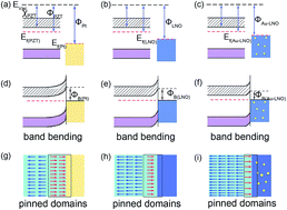
Metal-conductive oxide nanocomposite thin films are regarded as promising electrodes for ferroelectric devices to overcome the intrinsic drawbacks of conventional metal or conductive oxides electrodes. In this work, ferroelectric Pb(Zr,Ti)O3 (PZT) thin films with a thickness of 240 nm were deposited on metal-conductive oxide nanocomposite Au–LaNiO3 (Au–LNO) electrodes by a sol–gel method, and their microstructure and ferroelectric properties were investigated. It was observed that the PZT thin films fabricated on the Au–LNO bottom electrode exhibited enhanced ferroelectricity with the remnant polarization as high as 59.6 μC cm−2, which was much larger than those on the Pt (20 μC cm−2) and the LNO (33 μC cm−2) bottom electrodes. The J–V characteristics fitted by the Schottky emission model revealed the lowest potential barrier height at the interface between the PZT thin film and the Au–LNO electrode. The low potential barrier height contributed to a thin spacing charge layer at the PZT/Au–LNO interface, which was beneficial to the switching of ferroelectric domains. Ultraviolet photoelectron spectroscopy (UPS) results revealed that the decrease of the Schottky potential barrier was understood by the different work functions of the bottom electrodes according to the semiconductor theory. The present work demonstrates that metal-oxide nanocomposite electrodes can effectively improve the electrical properties of ferroelectric films by modulation of the Schottky potential barrier height. In particular, the modulation of the Schottky potential barrier by using nanocomposite electrodes also provides meaningful guidance for designing high performance ferroelectric photovoltaic devices.
Afterwards, the amorphous PZT thin films were deposited on the Au–LNO/SiO2/Si, the LNO/SiO2/Si and the Pt/Ti/SiO2/Si stacks by a general sol–gel process, respectively. The precursor solution for the PZT films was prepared from lead acetate (Pb(CH3COO)2), zirconium-n-propoxide (Zr(OCH2CH2CH3)4) and titanium tetra-isopropoxide (Ti((CH3)2CHO)4). 2-Propanol ((CH3)2CHOH) was used as the solvent. The final concentration of the solution was adjusted to 0.4 M with the atomic ratio of Pb:
Zr
:
Ti = 1.1
:
0.52
:
0.48. The PZT films were coated on the substrates by using a spin-coater, which operated at 1500 rpm for 10 s and then at 4000 rpm for 40 s. The coated films were dried at 120 °C for 5 min and then pyrolyzed at 250 °C for 5 min. The coating, drying and pyrolizing process were repeated once more, and then the perovskite PZT films with a thickness of 240 nm were obtained by annealing in an electric furnace at 600 °C for 30 min.
The crystal structure and orientation of the PZT films were analyzed by θ–2θ scans of X-ray diffraction (XRD; Rigaku RINT2000, Cu Kα radiation). The surface and cross-sectional morphologies of the PZT films were observed by scanning electron microscopy (FE-SEM; Supra 55, Ziess). The microstructures of the films were characterized by transmission electron microscopy (TEM; Tecnai G2 F20). The TEM specimens were prepared by the standard procedure of cutting, gluing, slicing, grinding and finally ion milling with Ar ions until they were electron transparent by using a Gatan precision ion-polishing system (PIPS 691; Gatan). Top electrodes of the Pt layer for electrical measurements were sputtered with a stainless iron mask with a diameter of 0.5 mm. The ferroelectric properties of the films were measured by using a standard ferroelectric testing system (TF2000E; Aixacct). The work functions of Pt, LNO and Au–LNO were measured by ultraviolet photoelectron spectroscopy (UPS) with He I discharge at hν = 21.22 eV and −5.6 V bias applied to the samples.
The surface morphology images of the PZT films deposited on the Pt (Fig. 2a), the LNO (Fig. 2c) and the Au–LNO (Fig. 2e) electrodes show well-crystallized PZT grains. All the PZT films exhibit smooth, uniform and dense microstructure and free from cracks or voids. The PZT films on the LNO and the Au–LNO bottom layers exhibit uniform grain size, which is estimated to be 100 nm. However, the PZT thin film on the metal Pt electrode displays uneven grain size. The difference in grain size distribution may be due to the different crystallization processes of the PZT films on different electrodes. In the case of the PZT films deposited on the perovskite-related oxides, the bottom layers can serve as nuclei seeds for PZT, so that the PZT grains can simultaneously grow along direction perpendicular to the surface with a uniform grain size. Otherwise, it experiences a nonuniform nucleation process when the PZT film deposited on the metal Pt electrode, which results in the PZT film consists of grains with different sizes. The cross-sectional SEM images show that the thickness of PZT films are around 240 nm, and a columnar grain structure predominates in all films (Fig. 2b, d and f). The more detailed microstructure of the PZT/Au–LNO interface was further investigated by TEM, and the results are shown in Fig. 3. Fig. 3a displays a low-magnification TEM image for the PZT film on the Au–LNO electrode, showing that columnar grains of the perovskite phase of PZT are grown on the bottom Au–LNO layer. The Au–LNO layer exhibits a microstructure that Au nanoparticles with an average size of 10 nm embedded uniformly in the LNO matrix, as shown in the inset. Fig. 3b shows a high-resolution TEM (HRTEM) image of the PZT/Au–LNO interface, which is clear without any interfacial layer (indicated by the red dashed lines). It has been reported that the interfacial amorphous layer between the ferroelectric film and bottom electrode may cause degradation of polarization and dielectric properties.23 Since Au nanoparticles are distributed uniformly in the LNO matrix, they can also appear at the top of the Au–LNO film. Thus, the Au nanoparticles have a large influence on the interface between PZT and the Au–LNO electrode. According to our previous work, the uniform distribution of Au nanoparticles can cause a change of valence band structure in the Au–LNO film, which results in the shift of Fermi level energy.20 Therefore, this may has a large influence on the energy band structure of the PZT/Au–LNO interface. The ferroelectric performance of the PZT thin film largely depends on the PZT/electrode interface, which will be discussed in detail subsequently.
![]() | ||
Fig. 2 Surface and cross-sectional SEM morphologies of the PZT thin films on the Pt (a, b), LNO (c, d) and Au–LNO electrodes (e, f), respectively. |
The ferroelectric properties of the PZT films on these three different electrodes were investigated, and the corresponding ferroelectric polarization (P–E) and switching-current (I–V) hysteresis curves are shown in Fig. 4. Fig. 4a reveals that the PZT films exhibit square P–E loops. The observed remnant polarization for the PZT film deposited on the Au–LNO electrode is as large as 59.6 μC cm−2, which is much larger than the values of the PZT films deposited on the Pt and LNO electrodes in this work, and other conductive oxides-buffered Si substrates.12,25–28 Usually, microstructures can influence the electric properties of ferroelectric films, therefore it is necessary to discuss whether the orientation, grain size and grain boundary are crucial for the enhancement in remnant polarization of the PZT film on the Au–LNO layer. Oikawa et al. reported that the ferroelectric properties of PZT films with the chemical composition near the morphotropic phase boundary (MPB) showed a strong orientation anisotropy: the PZT film with (111)-oriented showed the highest remnant polarization and the (100)-oriented film exhibited the lowest remnant polarization.29 In our case, the PZT film deposited on the Au–LNO layer with weakly (110)-preferred orientation shows the highest remnant polarization, whereas, the (111)-orientated PZT film on the Pt layer exhibits the lowest remnant polarization. Therefore, the enhancement in ferroelectric properties of the PZT film on the Au–LNO electrode cannot be explained by the preferred orientation. As shown in Fig. 2(c) and (e), the grain size in the PZT films on the LNO and Au–LNO electrodes is almost the same, but the remnant polarization of the PZT thin film on the Au–LNO electrode is higher than that on the LNO electrode. Vu et al. reported that grain boundaries also play an important role in the ferroelectric polarization of PZT thin films.30 In their work, the initial remnant polarization in the (110)-oriented PZT films is lower than those of the (001)-orientated PZT films, and after 1010 switch cycles, the remnant polarization in the (110)-orientated films gradually increases to the value of the (001)-orientated films.30 They think that this is ascribed to difference in the microstructure with a lower connectivity of grain boundaries. Since in the initial stage, the polarization in the (110)-orientated film is screened by grain boundaries. In this work, the initial remnant polarization in the weakly (110)-oriented PZT film on the Au–LNO electrode is higher than those of the (100)- and (111)-oriented PZT films on the LNO and Pt electrodes, which is different from Vu's results. As the switching cycle increases, the remnant polarization decreases, and begins to recovery after 109 cycles in the weakly (110)-oriented PZT film (not shown here). So in the initial stage of cycling, the polarization is not determined by the screening of grain boundaries. Therefore, it can be considered that microstructure does not play an critical role in the polarization of the PZT film on the Au–LNO electrode. The enhancement in the ferroelectric polarization may be related to the modification of interface potential between the PZT film and the Au–LNO electrode. As can be seen from Fig. 4a, all the PZT films exhibit asymmetry hysteresis loops. Although the coercive field Ec(−) under the negative voltage is almost the same for all cases (100 kV cm−1), the Ec(+) under the positive voltage is 110 kV cm−1, 130 kV cm−1 and 150 kV cm−1 for the PZT film on the Au–LNO, LNO and Pt electrodes, respectively. This difference may be related to switching behaviors of ferroelectric domains at the interfaces. To examine the switching dynamics of the domains, the I–V hysteresis curves of these three samples are displayed in Fig. 4b. One obvious difference is that the PZT film on the Au–LNO electrode shows two peaks in the I–V curve. According to the recent work of Guo et al., the peak at the lower electric field can be ascribed to the field-induced long-range order ferroelectric domains.31 Another obvious difference is that the switching current density of the PZT film on the Au–LNO electrode is higher than those of the other two samples. During the switching process of ferroelectric domains, the switching current is related to the growth rate of domain nuclei.32 In other words, the high switching current density represents a high growth rate of ferroelectric domain nuclei. The nucleation of ferroelectric domains largely depends on the effective electric field,32,33 and the switching current is proportional to the effective electric field. As we know, the effective electric field Eeff on the ferroelectric film can be obtained by Eeff = Eex − Ein, where Eex is the applied electric field, and Ein stands for a kind of coercive field including depolarized field and screening electric field induced by the space charge layer at the ferroelectric film/electrode interface. The different switching behaviors of the PZT films on different electrodes indicate that the effective electric field is different. Under the same electric field applied, the effective electric field is dependent on the thickness of the spacing charge layer at the ferroelectric thin film/electrode interface, which is related to the interface potential barrier height.
![]() | ||
Fig. 4 (a) Polarization–electric field (P–E) hysteresis loops. (b) Switching current–voltage (I–V) hysteresis loops of PZT films on the Pt, LNO and Au–LNO electrodes measured at 1 kHz. |
In order to investigate the potential barrier height at the interface between ferroelectric film and electrode in these samples, the leakage current at room temperature was also characterized, and the results are displayed in Fig. 5. From the experimental data, we observed that the J–V curves of the PZT films show a similar shape, and the positive and the negative branches are not identical. This asymmetry in the J–V curves suggests that the Poole–Frenkel (PF) emission from the traps is not suitable for this case, since the bulk-controlled mechanisms should be symmetric to the change of the voltage polarity.34 In addition, the PF model requires a situation of ohmic-like contacts on the insulator, which does not apply the PZT films on conductive oxides, such as LNO and SRO. The above observations hint toward an interface-controlled Schottky emission (SE) mechanism. Therefore, the leakage current density can be fitted by the following equation:35
![]() | (1) |
![]() | (2) |
The graphical representation ln(J/T2) − V1/2 should be a straight line as shown in Fig. 5b. It can be seen obviously that three samples show a similar slope, whereas, the intercepts differ from each other. We can obtain the value of potential barrier height from the intercept. From the fitting results, the obtained values of ΦB(Pt) − ΦB(LNO) and ΦB(LNO) − ΦB(Au–LNO) are 0.098 eV and 0.027 eV, respectively. The results reveal that the potential barrier height is the lowest at the PZT/Au–LNO interface among these three samples. The low Schottky potential barrier indicates a thin interface space charge layer, which is benefit for the switching of ferroelectric domains at the interface. Therefore, the PZT film on the Au–LNO electrode exhibits the prominent ferroelectric property.
To understand the difference in the Schottky potential barrier height of PZT films on these three electrodes, it is necessary to take consideration about the factors that play a role in determining the potential barrier. According to the semiconductor theory, the potential barrier height is dependent on the work functions of the bottom electrode and the ferroelectrics as well as electron affinity of the ferroelectrics. The Schottky potential barrier height can be obtained by the following equation:36
ΦB = S(ΦM − ΦS) + (ΦS − χS) | (3) |
![]() | (4) |
For the PZT thin film, S is calculated to be 0.266 based on the above equation by using a εop value of 6.25. We also investigated the work functions of these three bottom films by ultra-violet spectroscopy (UPS) as shown in Fig. 6. The Au–LNO film exhibits a work function of 4.8 eV, whereas the work function for the LNO and Pt electrodes is 4.9 eV and 5.3 eV, respectively. Thus, the potential barrier difference between the PZT/LNO and PZT/Au–LNO interfaces can be obtained to be 0.027 eV, while between the PZT/Pt and PZT/LNO interfaces is 0.10 eV. The results are consistent with the values obtained by fitting the leakage current density. Thus, the uniform distribution of Au nanoparticles in the LNO matrix can affect the Fermi level of the Au–LNO composite film, which in turn will affect the interface potential barrier height when the ferroelectric film is deposited on it. The lower Schottky potential barrier at the PZT/Au–LNO interface is induced by the thinner space charge layer at the interface compared with the PZT/Pt and PZT/LNO interfaces.
![]() | ||
Fig. 6 Work functions of (a) the Pt film, (b) the LNO film and (c) the Au–LNO nanocomposite film measured by UPS. |
Based on the above discussion, the energy band structures of the PZT/Pt, PZT/LNO and PZT/Au–LNO interfaces are drawn schematically in Fig. 7. Due to the Fermi level of the Au–LNO layer is higher than that of the LNO layer, the Au–LNO layer exhibits a smaller work function compared with the LNO layer (Fig. 7a–c). When the PZT films deposited on these three different bottom layers, the band bending in the PZT films is shown in Fig. 7d–f, respectively. The higher potential barrier at the Pt/PZT interface results in a thicker space charge layer. As mentioned above, the space charge layer causes the pinning of the ferroelectric domains at the interface between PZT film and electrode, so the density of the pinned domains (indicted by the red arrows) at the PZT/Au–LNO interface is lower compared with those at the PZT/LNO and PZT/Pt interfaces, as displayed in Fig. 7g–i. When the electric field is applied, the growth rate of domain nuclei in PZT film on the Au–LNO electrode is faster than those in the PZT films on the LNO and the Pt electrodes, which contributes to a higher switching current. Thus, the enhanced remnant polarization can be well explained by the low Schottky potential barrier height at the PZT/Au–LNO interface. The present results indicate that the modulation of Schottky potential barrier at the interface between ferroelectric film and electrode by using metal-oxide nanocomposite conductive electrode is an effective way to improve the performance of ferroelectric films.
This journal is © The Royal Society of Chemistry 2015 |