DOI:
10.1039/C5RA22381D
(Paper)
RSC Adv., 2015,
5, 105379-105392
Self-sacrifice Te template synthesis of new phase PbmSb2nTem+3n nanorods via Pb2+/Sb3+ synergistic effect†
Received
26th October 2015
, Accepted 16th November 2015
First published on 17th November 2015
Abstract
Nanocrystals have been attracted extra attention due to their unique characteristics, different from their bulk counterparts. Herein, we first synthesized the new stable phase of ternary PbmSb2nTem+3n one-dimensional (1D) nanorods with a rough surface, using Te as sacrificial template. X-Ray diffraction techniques (XRD), field emission scanning electron microscopy (FE-SEM) and energy-dispersive spectroscopy (EDS), X-ray photoelectron spectroscopy (XPS) analysis have been used to characterize and determine the structure and composition of the product. By carefully adjusting the experimental conditions, it was found that reaction factors including distinct solvent, the amount of alkali, reaction temperature, the ratio of reactants and growth time, play critical roles in the crystallization process of PbmSb2nTem+3n nanorods. Thorough morphological characterization revealed that significant variation of the morphology of the products originated from varying the amount of Pb/Sb precursors injected. Reaction with excess Pb produces PbmSb2nTem+3n nanocubes with size variations, whereas the initial morphology of the Te nanorod template with a rough surface was preserved in the presence of Sb. The Pb2+/Sb3+ synergistic effect was attributed to the difference of their reaction reactivity. A mechanistic model is proposed to account for these experimental findings. Furthermore, the optical band gaps (Eg) of PbmSb2nTem+3n were investigated as well.
1. Introduction
Tellurium, a narrow band semiconductor with a band gap of 0.3 eV, exhibits a trigonal phase. In its crystal structure, Te atoms are believed to be bound together through van der Waals interactions in a hexagonal lattice which leads to a very strong tendency towards anisotropic growth along the [001] direction, such as one-dimensional (1D) rods,1 wires,2 tubes3 etc. Recently, these 1D Te nanostructures have been further utilized as a template for synthesizing different binary 1D metal telluride nanostructures. For instance, Jeong and his co-workers reported that Te was transformed into Ag2Te by topotactic transformation and further changed to diverse ultrathin chalcogenide nanowires MxTey (M = Cd, Zn, Pb, and Pt) using a well-designed ion-exchange reaction,4 in which CdTe can be also fabricated directly from Te as template.5 Wu's research group have synthesized PbTe nanowires, Bi2Te3 nanowires and ultrathin metal telluride nanowires including Ag2Te, Cu1.75Te and PbTe using a safer reducing agent.6,7 Meanwhile, Bi2Te3 nanowires were obtained by cathodic stripping of a Te electrode by Yuan et al.8 Besides the homogenous structures that can be obtained from the Te template, plenty of heterostructures have been reported by some research groups, such as PbTe–Bi2Te3,9 Ag2Te–Bi2Te3,10 Te–Bi2Te3 nanostrings,11 barbells,12 and core/shell nanotubes.13 That Te–Ag2Te3 has two kinds of structures is mostly due to two mechanisms during the reactions; the well-known Kirkendall effect or topotactic transformation.14 Furthermore, Anirban Som et al. have prepared Ag2Te nanowires or Ag–Te heterostructures controlled by the difference in reactivity of a silver cluster in contrast to its ions and nanoparticles.15 However, except for TeCuPt and PtPdTe nanowires,16 efforts toward the facile synthesis and investigation of the ternary solid solution nanorods by Te templates have been rare.
Bulk lead telluride (PbTe), due to its narrow band gaps (0.32 eV) and face-centered cubic structure, has been applied widely in a number of fields such as photovoltaics, IR photoelectrics and thermoelectrics.17,18 In recent years, various morphologies of PbTe including quantum dots,19 nanofilms,18 nanosheets by self-assembly from nanoparticles,20 porous microstructures,21 nanocubes17,22 hierarchical nanostructures23–25 and nanowires/nanorods26 have been fabricated via multiple varied methods. On the other hand, alloying lead chalcogenides with a small amount of other semiconductor compounds for ternary or multinary compounds can increase the figure of merit by tuning the electrical transportant properties and the lattice thermal conductivity.27–30 However, different from alloying bulk materials through high temperature solid state reaction, there have not been many successes in the multinary PbTe-based semiconductor nanocrystals due to the “self-purification” of impurities,31 especially those with small size. In the “self-purification” mechanism, the impurity formation energy in nanocrystals is much higher than that in bulk materials. Furthermore, from a kinetic perspective, the distance impurities need to travel to reach the surface of the nanocrystals is very small. Both of these facts cause a decrease of solubility of dopant impurities in nanocrystals.31,32 Recently, there have been increasing numbers of ternary or multinary compounds examples in multicomponent chalcogenide systems; for example, Mn-doped PbSe self-assembled by the corresponding particles.33 Researched by Yalcin et al.34 showed that Ag2S acted as a transposition state and could be obtained from Ag nanowires which were finally transformed to AgFeS2 nanowires. Ajay Singh et al. doped Ga and Sb into CuInS with shape control via tuning the dosage of Ga, catalyzed by antimony,35 which was similar to PbSe–Bi nanorods assembled from PbSe particles using Bi as catalyst.36 Kadel et al. synthesized PbTe with In doping, in which In atoms were more likely to replace lead (Pb) rather than to take the interstitial sites.17
In addition, interestingly, Hao et al.37 discovered the existence of stable ternary rock-salt-based compounds: SrPb3S4, SrPbS2, and Sr3PbS4, in the PbS–SrS system, which were similar to Pb2−xSnxS2 nanocrystals and proved to phase-separate in the bulk phase.38 Kanatzidis' group achieved the nanoscale stabilization of new phases of PbmSb2nTem+3n nanoparticles39 and PbmSb2nSem+3n flower-like nanocrystals.40 A new phase of homologous PbmBi2nTe3n+m nanosheets was fabricated by Arindom Chatterjee et al.41 However, despite decades of investigations in understanding the growth mechanism of semiconductor nanostructures, the formation protocols of these multinary systems are not well known. The well-studied classical mechanism of nucleation followed by growth is mostly restricted to binary semiconductors but is not appropriate to multinary structures.42,43 To our best knowledge, there have to date been few examples in the literature that study new, stable phases of PbmSb2nTem+3n exhibiting nanorod morphology, except for the phases shown in the phase diagram39 (Fig. 1). PbmSb2nTem+3n nanorods can only exist at the nanoscale, which has been proved to be a PbTe–Sb2Te3 mixture in the bulk, except for PbSb4Te4 and PbSb2Te4.
 |
| | Fig. 1 Pseudobinary phase diagram of the PbTe–Sb2Te3 system. | |
Herein, we had prepared stable 1D PbmSb2nTem+3n bamboo-like nanorods by a solvothermal method via Te as sacrificial template. To the best of our knowledge, this is the first report of rod-shaped secondary structures. A two-step method that introduced the Pb source and Sb source simultaneously after the Te nanorod template had been generated completely was employed. The shape-dependence on the dosage of the Pb/Sb sources was discussed, which involved synergistic interaction between Pb2+ and Sb3+. Moreover, the formation mechanism was also studied compared to the one-step method during the chemical transformation.
2. Experimental
2.1. Synthesis
In a typical synthesis of PbmSb2nTem+3n nanorods by the solvothermal procedure, 0.320 g sodium selenite (Na2TeO3) and 0.250 g ethylenediaminetetraacetic acid disodium salt (EDTA) was added into a beaker containing 10 mL ethylene glycol. After constant electromagnetic stirring for 10 min with an injection of 4 mL hydrazine hydrate 80% (N2H4·H2O), the mixture was transferred into a 20 mL stainless Teflon-lined autoclave, sealed and maintained in an oven at a temperature of 180 °C for 0.5 h. The autoclave was cooled down to room temperature naturally after reaction and then 0.5 g lead acetate (Pb(CH3COO)2·3H2O), a series of doses of antimony potassium tartrate (K(SbO)C4H4O6·0.5H2O, 0.3 g for Sample 1; 1.0 g for Sample 2; 1.5 g for Sample 3), and 0.3 g potassium hydroxide (KOH) were added into a dry beaker, into which the products obtained above were transferred. After stirring for 15 min until all of the chemicals were dispersed thoroughly, they were transferred into a 20 mL stainless Teflon-lined vessel and heated to 180 °C for 5.5 h and cooled to room temperature. After that, the prepared sample was washed three times using pure water and ethanol, and finally dried in a vacuum oven at 80 °C for 4 h. All of the synthesis procedures and some of the photographs are shown in Fig. 2 and the elemental compositions, measured by ICP-AES, lattice parameters and mole Sb/total mole (Sb + Pb) values are shown in Table 1.
 |
| | Fig. 2 (a) Schematic diagram of reaction temperature vs. time during the synthesis of PbmSb2nTem+3n nanorods. (b) Digital photos before and after injecting N2H4·H2O. The solution in the beaker turned black, showing that the reduction reaction occurred. | |
Table 1 Elemental compositions, lattice parameters, and mole Sb/total mole (Sb + Pb) values
| Sample |
Pb (at%) |
Sb (at%) |
Te (at%) |
Composition |
Lattice parameter |
Mole Sb/total mole Sb + Pb |
| Sample 1 |
45.44 |
3.65 |
50.91 |
Pb12.44SbTe13.94 |
6.46142 |
0.074 |
| Sample 2 |
41.19 |
7.05 |
51.76 |
Pb5.84SbTe7.34 |
6.45869 |
0.146 |
| Sample 3 |
35.01 |
11.99 |
53.00 |
Pb2.91SbTe4.41 |
6.45558 |
0.256 |
2.2. Characterization
The X-ray diffraction (XRD) patterns of the products collected at room temperature were performed on a Rigaku D/max-2000 diffractometer equipped with Cu Kα radiation from 20° to 80° with a step of 0.02° and a scanning rate of 5° min−1; field emission scanning electron microscopy (FESEM), energy-dispersive X-ray spectroscopy (EDS; Quanta 200F) transmission electron microscopy, and high-resolution transmission electron microscopy (HRTEM, FEI, Tecnai G2 F30) were also used. Inductively coupled plasma-atomic emission spectroscopy (ICP-AES) was used to determine the elemental composition of the prepared series of PbmSb2nTem+3n nanocrystals. Only Pb2+ and Sb3+ were analyzed, as Te is liberated as H2Te gas during the dissolution process in aqua regia. The reported amounts of Te are only estimated, assuming charge-balanced compositions. The binding energy and surface oxidation of the prepared products were explored on the X-ray photoelectron spectrometer (XPS) (PHI 5700 ESCA40), using Al Kα radiation as the exciting source. The optical property of the products was performed with a Fourier transform infrared spectrometer (FTIR, Nicolet 5700).
3. Results and discussion
3.1. Structure and morphology characterization
The composition and phase of the as-prepared samples can be determined by the powder X-ray diffraction pattern (XRD), which was used to examine the crystal structure and the phase purity of materials whose XRD pattern is unique and definitely different from any others. As indicated in Fig. 3a, PbmSb2nTem+3n samples synthesized by the two-step method displayed pure phase and all the diffraction peaks can be indexed to PbTe of a face-centered-cubic (fcc) structure with the space group Fm![[3 with combining macron]](https://www.rsc.org/images/entities/char_0033_0304.gif) m (225) (JCPDS#38-1435), in which some diffraction peaks presented as (111), (200), (220), (311), (222), (400), (420), (422) and (511) planes, corresponding to the 2θ of 23.8°, 27.7°, 39.4°, 46.6°, 48.8°, 57°, 64.4°, 71.5°, 76.5°. The narrow and sharp peaks show their high crystallinity and no characteristic peaks peculiar to the source materials or other impurities were observed. As expected for the smaller ionic radius of Sb, (the radii of Sb and Pb are ∼1.45 Å and ∼1.80 Å, respectively), a gradual shift to higher 2θ was observed (Fig. 3a) as the Sb content in the PbmSb2nTem+3n alloys increased.44 The measured fine lattice parameters demonstrated a linear dependence as they decreased monotonically with increasing Sb content. This linear dependence was consistent with Vegard's law and demonstrated the compositional homogeneity of these PbmSb2nSem+3n alloys (shown in Fig. 3b). The Energy Dispersive Spectrometer (EDS) showed that the existence of Sb atoms in the PbTe matrix, was consistent with the XRD pattern (shown in Fig. 3c). Moreover, it determined the elemental composition of the prepared series of PbmSb2nSem+3n nanorods, whose data were similar to those measured by ICP-AES.
m (225) (JCPDS#38-1435), in which some diffraction peaks presented as (111), (200), (220), (311), (222), (400), (420), (422) and (511) planes, corresponding to the 2θ of 23.8°, 27.7°, 39.4°, 46.6°, 48.8°, 57°, 64.4°, 71.5°, 76.5°. The narrow and sharp peaks show their high crystallinity and no characteristic peaks peculiar to the source materials or other impurities were observed. As expected for the smaller ionic radius of Sb, (the radii of Sb and Pb are ∼1.45 Å and ∼1.80 Å, respectively), a gradual shift to higher 2θ was observed (Fig. 3a) as the Sb content in the PbmSb2nTem+3n alloys increased.44 The measured fine lattice parameters demonstrated a linear dependence as they decreased monotonically with increasing Sb content. This linear dependence was consistent with Vegard's law and demonstrated the compositional homogeneity of these PbmSb2nSem+3n alloys (shown in Fig. 3b). The Energy Dispersive Spectrometer (EDS) showed that the existence of Sb atoms in the PbTe matrix, was consistent with the XRD pattern (shown in Fig. 3c). Moreover, it determined the elemental composition of the prepared series of PbmSb2nSem+3n nanorods, whose data were similar to those measured by ICP-AES.
 |
| | Fig. 3 (a) Comparative XRD patterns of PbmSb2nTem+3n solid solution samples and standard PbTe powder shown as vertical lines; (b) a plot showing the variation of the cell parameters with a nominal atomic composition of PbmSb2nTem+3n nanocrystals following Vegard's law, (c) the EDS spectrum of Sample 1. | |
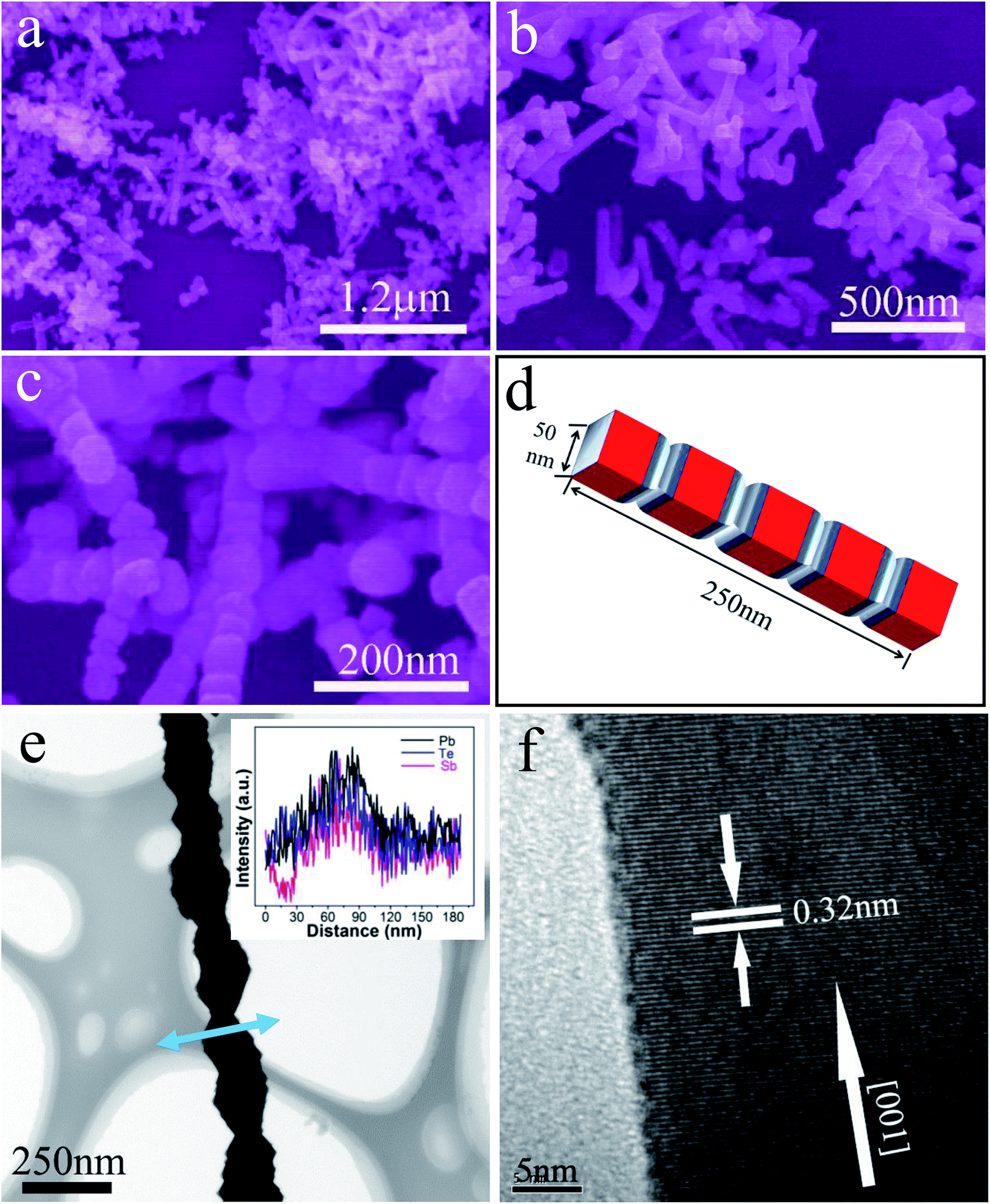
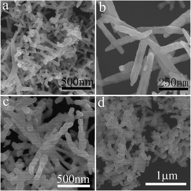
The morphology of the Sample 1 was studied by FESEM, as shown in Fig. 4, in which the low-magnification SEM images presented theoverall morphology of the products with homogeneous dispersion, uniform size and high yield (Fig. 4a and b). As in the high-magnification images (Fig. 4c), a number of bamboo-like nanorods appeared, which were likely to be assembled by four or five small cubes with length of 200 nm to 250 nm and a thickness of 40–50 nm. A 3D schematic diagram of such a bamboo-like nanorods is drawn in Fig. 4d. Moreover, the typical front-view line-scan EDS profile of a single nanorod, characterized by TEM (Fig. 4e), clearly shows the presence of all expected Pb, Te and Sb elements in thenanorod samples. The single phase homogeneity of the nanocrystals was further confirmed by the consistent rise and fall of Pb, Te, and Sb signals moving through the nanorods shown in the EDS line scan (inset in Fig. 4e). A HRTEM image taken from the PbmSb2nTem+3n nanorod edge was displayed in Fig. 4f and it can be seen that the interfringe distance in the single crystalline region is 0.32 nm, corresponding to the lattice spacing of the (100) planes in the cubic structure, showing that the nanorod axis is aligned with the [100] crystal direction. This is similar to the [200] axial direction observed in PbTe nanowires grown using two-step hydrothermal methods.45,46
 |
| | Fig. 4 (a–c) SEM images in different magnifications; (d) diagrammatic sketch of Sample 1; (e) TEM and (f) HRTEM images of Sample 1. | |
To date one dimensional, metal telluride nanostructures usually exhibited a smooth or rough surface which was attributed to different chemical conversion mechanisms under special synthetic conditions. Firstly, Fang et al. demonstrated that one dimensional (1D) corrugated nanoarrays of Pb(1−x)MnxSe nanocrystals formed through an in situ self-assembly process were based on the fundamental building blocks of octahedral nanocrystals.33 Pearl-necklace-shaped PbTe nanowires can be formed from the oriented attachment growth of spherical cubic PbTe nanoparticles and partially accompanied by Ostwald ripening to form nanowires with apartially smooth surface.47 Secondly, ultrathin (<15 nm) PbTe and Bi2Te3 nanowires in a low-cost solution-based process using Te nanowire templates would not have a rough surface due to their short diffusion pathway and the released strain.6,7 Thirdly, rough PbTe polycrystalline thermoelectric nanorods were fabricated through chemical transformation of Te nanorods.48 Therefore, a question came to be raised, what would the morphology of the samples really be? Were they bamboo-like nanorods with a semi-cube-like coarse surface or nanorods consisting of some senior cube units? In order to solve this problem, the growth mechanism of the nanorods is discussed in the following section.
The quality and composition of the as-prepared samples were further studied by X-ray photoelectron spectroscopy (XPS) analysis. Fig. 5a showed the XPS of the Sample 1 and Sample 3 with high resolution spectra of O 1s, Pb 4f, Te 3d and Sb 3d. The peaks at 142.28 eV and 137.43 eV in the high-resolution Pb 4f corresponding to Pb 4f2/5 and 4f7/2 with shoulder peaks on the high binding energy side (143.38 eV and 138.68 eV shown in Fig. 5b). Two components at 137.43 eV and 138.68 eV can be deconvoluted by reconvolution curve fitting (Fig. 5c and d), which corresponded to the expected chemical shifts for PbTe and either Pb(OH)2 or PbO.49 In addition, two sets of peaks at 540.13 eV, 530.88 eV were assigned to Sb 3d3/2 and Sb 3d5/2 respectively.50 From the Fig. 5e, the binding energy of Sb 3d of Sample 3 was stronger than those of Sample 1, which was attributed to the increasing dosage of Sb precursors. The Te 3d region had two groups of peaks, which were observed at 585.03 eV and 574.33 eV, indicating the existence of Te2− and either PbTe or Sb2Te3, and Te4+ (586.78 eV and 576.33 eV) due to a surface oxide layer.51 Notably, the oxide peaks of Sample 1 were stronger than those of Sample 3, shown in Fig. 5; we estimated that Sample 1 with rougher surface (Fig. 4c) would have a higher surface/volume ratio, which suggested that Sample 1 can be oxidized in an air atmosphere more easily than Sample 3, thereby increasing the proportion of PbO and Te4+ in Sample 1. Oxidation of PbTe is a complex, multistage process which is believed to start with the formation of peroxide-like structures and terminate in the formation of PbTeO3 on exposure to large O2 concentrations.52 For continuous surface oxide growth, oxygen atoms need to diffuse into the crystal and distort locally the perfect crystal structure, increasing disorder on the surface. A significant amount of oxygen is usually observed at the surface of PbTe NPs when exposed to air even during very short periods of time.53,54 In our case, a large surface-to-volume ratio of nanorods showed a high reaction reactivity with O2, because more dangling bonds of bare and uncoordinated metal sites (Pb, Sb) may exist due to extrinsic doping. Therefore, the surface of the product was covered by the amorphous thin oxide layer.
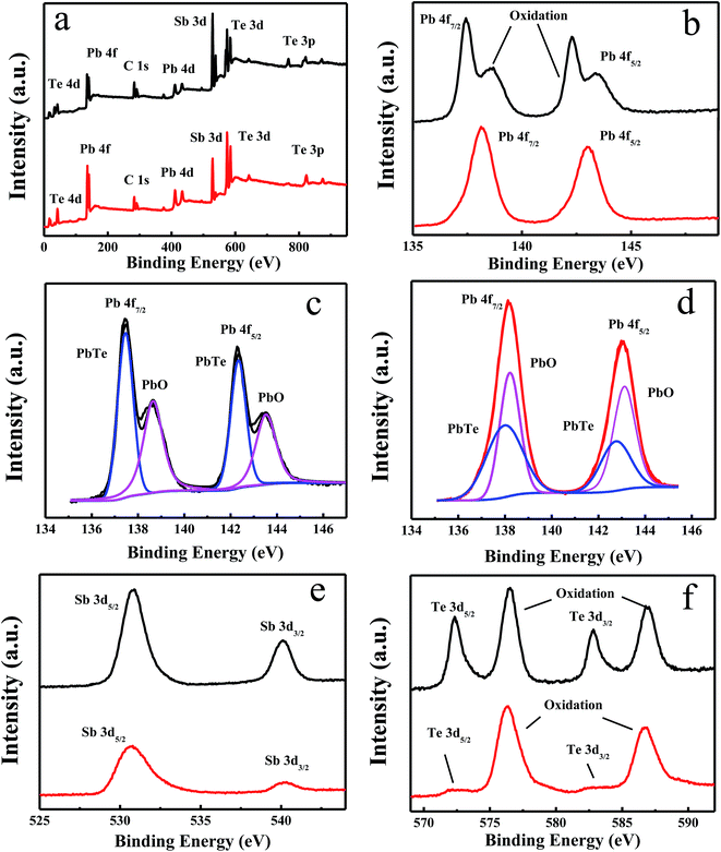 |
| | Fig. 5 X-Ray photoelectron spectroscopy (XPS) spectra for Sample 1 and Sample 3: (a) survey of the two samples; (b) high-resolution XPS peaks of Pb (4f), (e) Sb (3d) and (f) Te (3d) regions; (c and d) reference binding energies for PbTe and PbO are indicated at the bottom. | |
3.2. Investigation of parameters influencing the formation of PbmSb2nTem+3n nanorods
The shapes and structures of metal telluride (MxTey) nanocrystals can be influenced by a series of factors including the choice of solvent, reaction temperature, surfactant, reaction time, thermal regime, the molar ratio of the starting materials, reducing agents and so on. Therefore, we conducted experiments to examine the factors affecting the morphology changes of products on different reaction conditions.
3.2.1 The influence of solvent. Recently studies have shown that the reaction solvent is the one of keys to be able to control predictably the crystal and film growth by affecting the reaction process to change the viscosity, polarity, ion transfer rate and other characteristics.55,56 Herein, in order to explain the importance of ethylene glycol (EG) in generating the nanorod-shape of Sample 1, a group of experiments were conducted by varying the solvent mixtures (mixing other solvents with EG) at different ratios while keeping other conditions constant. The influence of the solvents on the morphology and structure of crystals were examined by SEM (Fig. S1†). Only nanocubes with a size of 50–80 nm appeared when a mixed solvent of di-n-propylamine/EG and ethanediamine (EA)/EG was used at a ratio of Vdi-n-propylamine![[thin space (1/6-em)]](https://www.rsc.org/images/entities/char_2009.gif) :VEG = 1:1 and VEA:VEG = 1:1 (Fig. S1a and b†). At a mixed EG and H2O solvent ratio of VH2O:VEG = 1:1, and even when using pure water as the solvent, a mass of nanorods with a smoother surface compared to the Sample 1 were obtained (Fig. S1c and d†). The solvent–solute and solvent–solvent interactions are very important chemical properties that have a large impact on the chemical reactions taking place. They can induce complex reactions among different solvents and different reactants, which finally lead to the existence of various structures and shapes. Non-aqueous solvents with higher viscosity allow self-assembly to occur at different rates, forming various morphologies in different solvents,57,58 which affect the solubility, reactivity and diffusion behavior of the reagents and the intermediates.59 Thus, given what we had discussed above, it is apparent that an optimal mixed solvent is indispensable to the formation of PbmSb2nTem+3n and it can be clearly seen that the bamboo-like rods could only be synthesized using pure EG as solvent.
:VEG = 1:1 and VEA:VEG = 1:1 (Fig. S1a and b†). At a mixed EG and H2O solvent ratio of VH2O:VEG = 1:1, and even when using pure water as the solvent, a mass of nanorods with a smoother surface compared to the Sample 1 were obtained (Fig. S1c and d†). The solvent–solute and solvent–solvent interactions are very important chemical properties that have a large impact on the chemical reactions taking place. They can induce complex reactions among different solvents and different reactants, which finally lead to the existence of various structures and shapes. Non-aqueous solvents with higher viscosity allow self-assembly to occur at different rates, forming various morphologies in different solvents,57,58 which affect the solubility, reactivity and diffusion behavior of the reagents and the intermediates.59 Thus, given what we had discussed above, it is apparent that an optimal mixed solvent is indispensable to the formation of PbmSb2nTem+3n and it can be clearly seen that the bamboo-like rods could only be synthesized using pure EG as solvent.
3.2.2 Effect of temperature. The synthetic temperature, as an essential reaction parameter, can have an obvious influence on the shapes and structures of the final products. Some examples from the literature reported that the morphology and size of PbTe crystals are sensitive to the synthetic temperature. For example, Wang's research group obtained different shapes of PbTe including tiny particles, nanocubes, nanocubes with spiral steps and dendrites with spiral step hollow cubic centers via ranging the temperature from 100 °C to 160 °C.24 In our case, distinct morphologies can be fabricated at 120 °C, 140 °C and 200 °C, respectively, without changing any other experimental conditions (Fig. 6). When the reaction temperature was 120 °C, SEM images revealed that nanopores were obviously observed throughout the nanorods (Fig. 6a and b). Increasing the temperature to 140 °C, a mixture of nanorods and broken nanotubes was acquired instead (Fig. 6c). Both the nanorods and nanotubes had disappeared and nanocubes with a size of about 1 μm could be observed when the temperature reached 200 °C (Fig. 6d).
 |
| | Fig. 6 SEM images of samples synthesized under different temperatures: (a and b) 120 °C; (c) 140 °C; (d) 200 °C. | |
On the basis of the above experimental results, the production of porous nanotubes was favored at lower temperature due to the nanoscale Kirkendall effect. The nanoscale Kirkendall effect is a general phenomenon,60,61 and this research field had recently been reviewed by Wang et al.62 As we know, the different diffusion rates of Te outward from the internal regions of nanorods and Pb2+/Sb3+ inward directly cause hollow structures. It is well known that EDTA or ethylenediaminetetraacetic acid is a novel molecule for complexing metal ions. The formation constant for the Pb–EDTA complex is reported to be 10.63 Pb2+/Sb3+ could react with EDTA to form a relatively stable [Pb(EDTA)] and [Sb(EDTA)+] complex. It is suggested that Pb2+/Sb3+ diffusion rates inward would be slower than Te diffuse outward because of the generation of isolated, highly active Pb/Sb ions is suppressed. Pb/Sb ions first nucleate selectively at the side-surface of the Te nanowires, which subsequently causes the formation of a Pb/Sb–Te alloy layer on the surface of the Te nanowires; non-equalizing diffusion between Pb/Sb and Te through the layer leads to void formation between the Pb/Sb–Te alloy layer and the core Te nanowires. Next, the Te core nanowires disappear through continuous mass transport and highly crystalline nanotubes were finally obtained. Raising the temperature to 140 °C, the [Pb(EDTA)] and [Sb(EDTA)+] complex can accelerate greatly the generation of Pb/Sb ions. According to the Fick rule: J = −D(dC/dx), J is the diffusion flux, D is the diffusion coefficient, and (dC/dx) is defined as the concentration gradient. In this case, J increases due to the improvement of the concentration gradient caused by releasing a mass of Pb/Sb ions from the coordination compound, thereby leading to the fast diffusion of Pb2+/Sb3+ inward into the Te matrix. On the other hand, the rate of ion diffusion was relatively fast with respect to that of crystal growth, upon the ion-exchange reaction, solid nanorods become nanoporous hollow rod-like products. At a higher temperature of 200 °C, Te nanorods had a quick tendency to dissolve into Te2− in a basic environment. Of course, another possibility that should be considered is lower melting point of Te nanorods compared to that of Te bulk (421 °C). Then, Pb–Sb–Te cubes/particles can generate both Te2− with Pb2+/Sb3+ directly through homogeneous nucleation. In our present work, different shaped crystals may be related to the diffusion rate of the ions and the growth rate of the crystals based on the concentration gradient around the interface of Te nanorods. Thus, the optimal reaction was maintained at 180 °C for 5.5 h which can lead to the uniform and nearly bamboo-like pure PbmSb2nTem+3n nanorods.
3.2.3 Effect of the amount of KOH. Besides the synthetic temperature discussed above, the amount of OH ions is another reaction factor which plays a significant role in the fabrication of the PbmSb2nTem+3n crystals. Herein, a group of experiments were designed except for the variation of KOH concentration. All the samples were prepared under the same reaction conditions as shown in the typical synthesis process. Without KOH, several smooth nanorods were observed, as shown in Fig. 7a and b. When the amount of KOH was 0.1 g (1.79 mmol), the nanorods with small fractures appeared be coarse (Fig. 7c). Furthermore, increasing the amount of KOH to 1.5 g (26.79 mmol) (Fig. 7d), many nanorods were obtained instead. It was reasonable to conclude that the amount of KOH played a crucial role in the reaction equilibrium existing in the following reaction process.| | |
3TeO32− + 3N2H4 → 3Te + 3N2 + 3H2O + 6OH−
| (1) |
| | |
3Te + 6OH− → 2Te2− + TeO32− + 3H2O
| (2) |
 |
| | Fig. 7 SEM images of samples synthesized with different amounts of KOH (a and b) 0 g (0 mmol), (c) 0.1 g (1.79 mmol), (d) 1.5 g (26.79 mmol). | |
Firstly, TeO32− was reduced by N2H4·H2O and sufficient Te atoms with high activity were prepared according to eqn (1); OH ions could transform Te into Te2− and corrode the Te nanorods according to eqn (2). When the reaction was carried out without OH ions, the chemical reaction route was mainly eqn (1), and the samples maintained their nanorod shape via heterogeneous nucleation. When a little KOH was present in the reaction system, Te atoms were partly converted into Te2− and TeO32− through eqn (2), which caused some fractures to be generated on the surface. When an excess of KOH was added, Te2− and TeO23− were continuously generated and subsequent nanocubes were obtained through homogeneous nucleation in which Te2− reacted with Pb2+/Sb3+. Based on the above discussions, we can conclude that the KOH used in the preparation would play a vital role in adjusting the chemical reaction route and further influencing the nucleation and growth of PbmSb2nTem+3n nanostructures.
3.2.4 Effect of the amount of metal precursors. The presence of Pb and Sb precursors, which reacted with the parent Te nanorods in the first step, can finally generate the target products. The variation of the amount of Sb precursors has been investigated and is shown in Fig. 8. When Sb precursors were absent, Te nanorods only reacted with Pb and finally generated a number of nanocubes with sizes of 50–100 nm (Fig. 8a). Unquestionably, PbTe nanocrystals, as we know, posses an average NaCl structure with a mix of eight {111} and six {100} faces to minimize the total surface energy and its crystallite is determined by the ratio of the growth rate of [100] to that of [111]. As the result of the intrinsic surface energy of (111) face being higher than all of the {100} faces, PbTe cubes are more likely to be obtained due to the faster growth rate in the (111) face. If the amount of Sb precursors was increased to 1.0 g (Fig. 8b, Sample 2), the nanorods were smoother than the Sample 1. With further increase of the amount of Sb precursors to 1.5 g (Fig. 8c, Sample 3), nanorods with a smoother surface can be seen. However, in the presence of an excess of Sb precursors (2.0 g) (Fig. 8d), it was clear that a mixture of several hexagonal plates (marked by arrows) and a mass of nanocubes with sizes of 30–50 nm appeared. Sb2Te3 has preferentially presented hexagonal plates due to its layered crystal structure in some previous studies.11,64 No matter by how much the amount of Sb precursor is increased (0.3–1.5 g), the samples showed the PbTe phase, indicating that Sb atoms were more likely to replace Pb and be incorporated into the PbTe matrix. Clearly, the introduction of Sb precursors would evoke the competition reaction between Pb2+/Sb3+ and Te nanorods. Here, the existence of Sb resources could occupy a number of reaction sites on the Te nanorods and block the pathway of Pb ions from one position to another. Therefore, antimony could perform as a kind of “inactive ion” compared to Pb ions. Previous study, R. J. Behm et al.'s work, had revealed that Ag atom was reduced due to the effect of site blocking (surface diffusion barrier) by the Sb atoms.65 This reduces the Ag diffusion constant linearly with the amount of Sb. Consequently, the main reaction (eqn (3)) had been suppressed and this decreased further the rate of heterogeneous nucleation, which restrained the formation of cubic crystal structures and kept the morphologies of nanorods unchanged. Furthermore, it seemed that there would be a threshold value of the Sb precursor amount, which can evoke the eqn (4) and be generated in quantity. Meanwhile, the nanocubes with sizes of 30–50 nm (Fig. 8d insert) were smaller than their counterparts without the addition of Sb precursors (about 50 nm, as shown in Fig. 8a), which was attributed to the consumption of Te via eqn (4). Above all, different amounts of Sb precursors can influence the reaction and finally determine the shapes and structures of the products.| | |
3Te + 2Pb2+ + 6OH− → 2PbTe + TeO32− + 3H2O
| (3) |
| | |
6Te + 3N2H4 + 4Sb3+ + 12OH− → 2Sb2Te3 + 3N2 + 12H2O
| (4) |
 |
| | Fig. 8 SEM images of as-prepared samples synthesized with different amounts of metal source: Sb source at (a–d) 0 g; 1.0 g; 1.5 g; 2.0 g; Pb source at (e, g, h) 0 g; 1.0 g; 1.5 g; (f) XRD pattern of as-prepared samples without Pb source. | |
In order to investigate further the role of metal precursors in forming bamboo-like nanorods, varying the amount of Pb precursors with a fixed concentration of Sb3+ was performed. When increasing the amount of Pb from 0 g to 0.5 g, the product shape evolved from hexagonal plates with a number of spherical particles to bamboo-like nanorods (Fig. 8e). Based on the XRD results (Fig. 8f), the powders obtained in the absence of Pb precursors corresponded to Sb2Te3 (PDF#72-1990) and excess Te (PDF#36-1452). As the Pb concentration was further increased from 1.0 g to 1.5 g (Fig. 8g and h), most of the nanocrystals were nanocubes with sizes of about 50 nm. It was similar to the case of the absence of Sb, in which excess Pb2+ would generate strong ion diffusion and show a higher reaction activity toward Te nanorods, resulting in the nanocubes. Obviously, bamboo-like nanorods can't form in the presence of Pb2+ or Sb3+ alone. We cannot ignore any species' role in tuning the nanocrystals’ morphology to form bamboo-like nanorods due to the synergistic interaction between Pb and Sb. Recent studies showed that the incorporation of dopants into the host lattices not only altered the composition of the nanocrystals but also modified the nanocrystal nucleation and growth rates, ultimately impacting the final morphology of the nanocrystal. Through adsorption onto the growth facets and tuning the rate of the chemical reaction processes, dopants can catalyze or slow down or even stop the directional growth of the nanomaterials, and they can also change the phase as well as the shape of some nanostructures. Recently, this impact of Sb on the reactivity of the gallium precursor has been shown to be potentially useful for the synthesis of CuIn1−xGaxS2 (CIGS) nanocrystals.35 By systematically tuning the amount of Sb3+ ion added, the influence of the dopant on shape is indirect; antimony catalyzes the incorporation of gallium. In our present work, the diffusivity and chemical reactivity of the Pb adatoms on the Te nanorod is reduced when the Sb atoms, even low amount of Sb precursor, act as repulsive impurities. Actually, based on the SEM images observed in Fig. 8a–d, the surface of the synthesized solid solution PbmSb2nTem+3n nanorod tends to be smoother with an increase in the amount of Sb precursor. Of course, a minimum Sb ratio determining the switch of nanocube and nanorod needs further investigation in the future. Consequently, generating the bamboo-like shapes needs two essential factors. Firstly, Pb and Sb sources must co-exist to react with Te nanorods via a cooperative effect. Secondly, it was necessary to keep the dosage of Pb and Sb sources to a reasonable range, which was able to control the ion diffusion and reaction activity toward Te, leading to retention of the shape of the parent nanorod template.
4. Growth mechanism
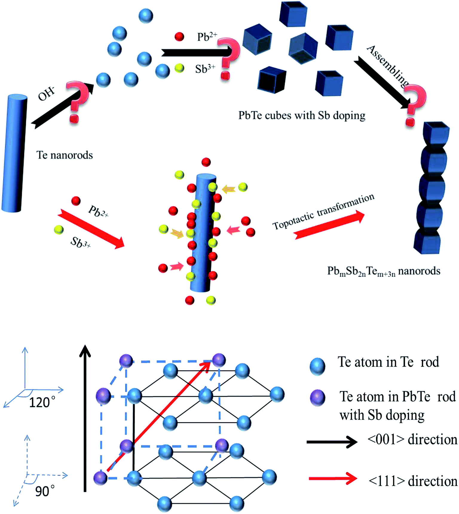
It was quite obvious that the reaction during the second step had an important influence on the final structure. What happened after the Pb/Sb precursors were adding to the reaction system and which structure should the products be? Were they transformed from the Te nanorods or assembled by certain small nanocubes? Thus, two hypotheses about the mechanisms of PbmSb2nTem+3n crystal growth have been put forward (Fig. 9): (1) the alkali existing in the solution corrodes the Te nanorods constantly until Te atoms are transformed into Te2−, which could react with Pb2+/Sb3+ to generate PbmSb2nTem+3n nanocubes through homogeneous nucleation. While the reaction was ongoing, PbmSb2nTem+3n nanorods become involved in the spontaneous arrangement and alignment of PbmSb2nTem+3n nanocubes via an oriented attachment process. (2) Pb/Sb ions diffused into the Te structure and reacted with Te to form a PbTe phase in the Te matrix via topotactic transformation.
 |
| | Fig. 9 (a) Schematic illustration of the proposed growth mechanisms of the Pb12.44SbTe13.94 nanorods for hypothesis 1 (along black arrows with question marks) and hypothesis 2 (along red arrows); (b) the angles and relative positions between Te–Te and the growth directions change during topological transformation from the Te hexagonal phase to PbTe fcc phase. | |
To further understand the growth mechanism of such Sample 1 bamboo-like nanorods? A time-dependent experiment in the second step was carried out. Before the conversion, Te nanorods were produced and analyzed at the first step according to the eqn (1). From the SEM images, it can be seen that the Te products had a 1D acicular nanorod with a relatively smooth surface, which had an average length of 500 mm and an average diameter of 50 nm (Fig. 10a). Trigonal tellurium (t-Te) tends to grow one-dimensional structures along the c-axis due to its highly anisotropic crystal structure consisting of helical chains of covalent boned atoms. The XRD pattern (Fig. 10b) can be indexed as Te without any other impurity. At the initial stage (2 h) (Fig. 10c), the products were composed of small, regular, smooth rods. With the increase of the growth period to 4 h (Fig. 10d), bamboo-like nanorods began to appear, showing pits that were due to topotactic transformation that had taken place and caused surface cracking. When Pb ions were incorporated into the Te nanorods from the outside to inside to form the PbTe phase, the [001]-directed hexagonal Te was transformed into [111]-directed fcc. This changed the angle between Te atoms from 120° to 90° at the 〈110〉 plane, perpendicular to the c-axis, thereby leading to a large lattice strain. The accumulated stress was released by cracking the surface and even breaking the nanorods during the transformation and generating shorter nanorods, which can be proved by the SEM images, which show that the as-prepared products with an average length of 250 nm were shorter than Te nanorods with the average length of 500 nm (Fig. 10e and f). Subsequently, after 8 h, there were two co-existing structures: nanorods and nanocubes that the cracked surface further broke into (Fig. 10g). Finally, when the reaction time was extended to 72 h, the pits developed into larger and deeper holes and the nanorods broke completely into a mass of nanocubes, via relieving the lattice strain accumulated during topotactic transformation (Fig. 10h).
 |
| | Fig. 10 SEM images of samples obtained by solvothermal treatment after introducing the Pb source and Sb source for different time intervals: (a) 0 h, (c) 2 h, (d) 4 h, (e) 5.5 h, (g) 8 h, (h) 72 h; (b) XRD pattern of Te nanorods synthesized at 0 h; (f) average length of Sample 1 nanorods decreased as compared to that of Te nanorods. | |
For the hypothesis (1): the Te nanorods were deconstructed by KOH to generate Te2− reacting with Pb2+/Sb3+, which undoubtedly denied the importance of the first step which generated Te nanorods and which was separate from the second step. Based on the above results, hypothesis (1) can be excluded. In addition, to further invalidate this hypothesis, a one-pot method was investigated and its SEM image shown in Fig. S2.† The existence of plentiful nanocubes rather than nanorods can also demonstrate that hypothesis (1) was not suitable in this system. Therefore, the present chemical transformation was based on hypothesis (2) through topotactic transformation.
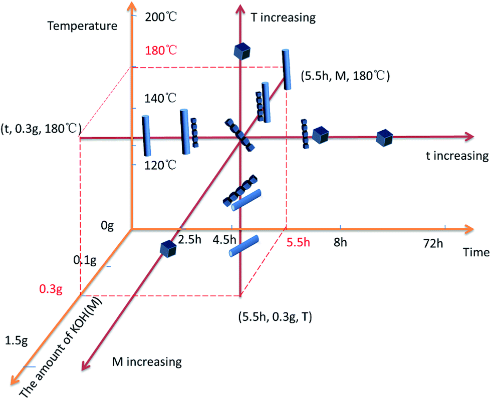
On the basis of experimental results, different crystal morphologies are shown in Fig. 11. These indicated that PbmSb2nTem+3n structures with certain morphologies had the same tendency, they performed as different morphologies from 1D nanorods/tubes to 3D nanocubes, with increasing amount of KOH, time and temperature, respectively. The details of the reaction mechanism need further clarification.
 |
| | Fig. 11 The tendency of Sample 1 crystal morphologies from 1D nanorods/tubes to 3D nanocubes with increasing the amount of KOH, time and temperature, respectively. | |
5. Optical properties
To study further the optical properties of the PbmSb2nTem+3n nanorods obtained in the typical synthesis route, they were investigated with FI-IR spectrometry and exhibited the well-defined band gap energies shown in Fig. 12. The electronic transition between the valence band and the conduction band for a direct band-gap material is given by (αhν)2 − (hν − Eg), in which “α” is the optical absorption coefficient, “h” is Planck's constant, “ν” is the frequency of the incident radiation, “hν” is the incident photon energy and “Eg” is the energy gap. Eg can be estimated by extending the linear part of the curve to zero absorption (Fig. 12). The band gap value of the Sample 1, Sample 2 and Sample 3 can be calculated to be 0.316, 0.341 and 0.375 eV, respectively. These band gap values were all bigger than the previously reported values for binary PbTe dendritic structures (0.272 eV),66 hopper crystals (0.268 eV) and nanowires (0.308 eV) in our previous work.25 On the other hand, the band-gap energies of the PbmSb2nTem+3n nanorods are significantly smaller than the literature values, in the range of 0.41–0.45 eV for ternary PbmSb2nTem+3n nanocrystals with a particle size of 10–12 nm, and those of pure PbTe nanocrystals with a size of about 10 nm (∼0.43 eV).39 By comparison, these values are significantly different from the band gaps of the individual binary end members, which are 0.28 eV for PbTe and 0.11 eV for Sb2Te3, and two distinct PbTe-based compounds PbBi2Te4 and PbBi6Te10 samples (0.7 and 0.25 eV), respectively.41 Interestingly, the band gap value of Sample 1 is close to the literature value (0.31 eV) for PbTe nanoparticles prepared by Zhu's research group and the latter are expected to be blue-shifted by quantum confinement relative to their bulk parent.67 Meanwhile, it was clearly observed that Sample 3 showed a higher band gap value than Sample 1 and Sample 2; it has been widely accepted that an increase in the amount of dopant is accompanied by changes in the optical properties.68 In fact, it is well known that PbTe has the largest Bohr radius of any crystalline semiconductor. In particular, the anisotropy in PbTe is quite pronounced and quantum confinement effects will be felt in PbTe NCs with a longitudinal Bohr radius (152 nm).69
 |
| | Fig. 12 Plot of (αhv)2 versus hv for determination of the band gap of Sample 1, Sample 2 and Sample 3; the insets are the corresponding SEM images. | |
6. Conclusion
In summary, we first put forward a solvothermal method to synthesize metastable nanoscale phase PbmSb2nTem+3n (Pb12.44SbTe13.94, Pb5.84SbTe7.34, Pb2.91SbTe4.41) nanorods. Pb12.44SbTe13.94 bamboo-like nanorods were formed through topological transformation instead of assembly by several individual nanocubes. The products can only be obtained via a two-step method rather than a one-step method. Sb precursors can occupy the site that should have been occupied by Pb and block the Pb diffusion pathway, thereby leading to the nanorod shape. The interfacial interaction between Pb, Sb species and the Te crystal surface can successfully change the growth nature of the crystals due to a Pb2+/Sb3+ synergistic effect. Due to the strong quantum confinement effect, the band gap value of the Sample 1, Sample 2 and Sample 3 can be calculated to be 0.316, 0.341 and 0.375 eV, respectively. The method may be extended to the control of crystallization and the formation of other one-dimensional multicomponent PbTe-based alloy compounds.
Acknowledgements
This work was supported by the National Natural Science Foundation of China (Project No. 21101044), the Independent Subject of the State Key Laboratory of Advanced Welding and Joining and the Fundamental Research Funds for the Central Universities (Grant No. HIT. NSRIF. 2013076 and IBRSEM. 201330) and Program for Innovation Research of Science in Harbin Institute of Technology (PIRS of HIT No. B201507).
References
- Z. Liu, Z. Hu, J. Liang, S. Li, Y. Yang, S. Peng and Y. Qian, Langmuir, 2004, 20, 214 CrossRef CAS PubMed.
- Y. J. Zhu, W. W. Wang, R. J. Qi and X. L. Hu, Angew. Chem., 2004, 116, 1434 CrossRef.
- A. Qin, Y. Fang, P. Tao, J. Zhang and C. Su, Inorg. Chem., 2007, 46, 7403 CrossRef CAS PubMed.
- G. D. Moon, S. Ko, Y. Xia and U. Jeong, ACS Nano, 2010, 4, 2307 CrossRef.
- H. W. Liang, S. Liu, Q. S. Wu and S. H. Yu, Inorg. Chem., 2009, 48, 4927 CrossRef CAS.
- S. W. Finefrock, H. Fang, H. Yang, H. Darsono and Y. Wu, Nanoscale, 2014, 6, 7872 RSC.
- H. Yang, S. W. Finefrock, J. D. Albarracin Caballero and Y. Wu, J. Am. Chem. Soc., 2014, 136, 10242 CrossRef CAS.
- G. Yuan, Y. Li, N. Bao, J. Miao, C. Ge and Y. Wang, Mater. Chem. Phys., 2014, 143, 587 CrossRef CAS.
- H. Fang, T. Feng, H. Yang, X. Ruan and Y. Wu, Nano Lett., 2013, 13, 2058 CrossRef CAS PubMed.
- H. Fang, H. Yang and Y. Wu, Chem. Mater., 2014, 26, 3322 CrossRef CAS.
- Y. Zhang, H. Chen, Z. Li, T. Huang and S. Zheng, J. Cryst. Growth, 2015, 421, 13 CrossRef CAS.
- W. Wang, J. Goebl, L. He, S. Aloni and Y. Hu, J. Am. Chem. Soc., 2010, 132, 17316 CrossRef CAS PubMed.
- Z. Li, S. Zheng, T. Huang, Y. Zhang, R. Teng and G. Lu, J. Alloys Compd., 2014, 617, 247 CrossRef CAS.
- K.-R. Park, S. Kim, N. V. Myung, S.-O. Kang and Y.-H. Choa, RSC Adv., 2015, 5, 29782 RSC.
- A. Som, A. K. Samal, T. Udayabhaskararao, M. S. Bootharaju and T. Pradeep, Chem. Mater., 2014, 26, 3049 CrossRef CAS.
- H. Li, C. Ren, S. Xu, L. Wang, Q. Yue, R. Li, Y. Zhang, Q. Xue and J. Liu, J. Mater. Chem. A, 2015, 3, 5850 CAS.
- K. Kadel, L. Kumari, X. Wang, W. Li, J. Y. Huang and P. P. Provencio, Nanoscale Res. Lett., 2014, 9, 227 CrossRef PubMed.
- J. Si, J. Zhao, G. Ding and H. Wu, Appl. Surf. Sci., 2014, 321, 233 CrossRef CAS.
- A. Khiar, M. Eibelhuber, V. Volobuev, M. Witzan, A. Hochreiner, H. Groiss and G. Springholz, Opt. Lett., 2014, 39, 6577 CrossRef CAS.
- T. J. Zhu, X. Chen, X. Y. Meng, X. B. Zhao and J. He, Cryst. Growth Des., 2010, 10, 3727 CAS.
- P. K. Rawat and P. Banerji, RSC Adv., 2014, 4, 29818 RSC.
- J. Zhou, Z. Chen and Z. Sun, Mater. Res. Bull., 2015, 61, 404 CrossRef CAS.
- Z. Quan, Z. Luo, Y. Wang, H. Xu, C. Wang, Z. Wang and J. Fang, Nano Lett., 2013, 13, 3729 CrossRef CAS PubMed.
- Q. Wang, G. Chen and H. Yin, J. Mater. Chem. A, 2013, 1, 15355 CAS.
- H. Yin, Q. Wang and G. Chen, Chem. Eng. J., 2014, 236, 131 CrossRef CAS.
- S. W. Finefrock, G. Zhang, J. H. Bahk, H. Fang, H. Yang, A. Shakouri and Y. Wu, Nano Lett., 2014, 14, 3466 CrossRef CAS PubMed.
- L. D. Zhao, S. H. Lo, J. He, H. Li, K. Biswas, J. Androulakis, C. I. Wu, T. P. Hogan, D. Y. Chung, V. P. Dravid and M. G. Kanatzidis, J. Am. Chem. Soc., 2011, 133, 20476 CrossRef CAS PubMed.
- L. D. Zhao, J. He, S. Hao, C. I. Wu, T. P. Hogan, C. Wolverton, V. P. Dravid and M. G. Kanatzidis, J. Am. Chem. Soc., 2012, 134, 16327 CrossRef CAS.
- K. Biswas, J. He, Q. Zhang, G. Wang, C. Uher, V. P. Dravid and M. G. Kanatzidis, Nat. Chem., 2011, 3, 160 CrossRef CAS PubMed.
- K. Biswas, J. He, I. D. Blum, C. I. Wu, T. P. Hogan, D. N. Seidman, V. P. Dravid and M. G. Kanatzidis, Nature, 2012, 489, 414 CrossRef CAS PubMed.
- G. M. Dalpian and J. R. Chelikowsky, Phys. Rev. Lett., 2006, 96, 226802 CrossRef.
- M. H. Du, S. C. Erwin, A. L. Efros and D. J. Norris, Phys. Rev. Lett., 2008, 100, 179702 CrossRef PubMed.
- W. Lu, P. Gao, W. B. Jian, Z. L. Wang and J. Fang, J. Am. Chem. Soc., 2004, 126, 14816 CrossRef CAS.
- B. Sciacca, A. O. Yalcin and E. C. Garnett, J. Am. Chem. Soc., 2015, 137, 4340 CrossRef CAS PubMed.
- A. Singh, A. Singh, J. Ciston, K. Bustillo, D. Nordlund and D. J. Milliron, J. Am. Chem. Soc., 2015, 137, 6464 CrossRef CAS PubMed.
- M. S. Kim and Y. M. Sung, CrystEngComm, 2012, 14, 1948 RSC.
- S. Hao, L. D. Zhao, C. Q. Chen, V. P. Dravid, M. G. Kanatzidis and C. M. Wolverton, J. Am. Chem. Soc., 2014, 136, 1628 CrossRef CAS PubMed.
- R. B. Soriano, C. D. Malliakas, J. Wu and M. G. Kanatzidis, J. Am. Chem. Soc., 2012, 134, 3228 CrossRef CAS PubMed.
- R. B. Soriano, I. U. Arachchige, C. D. Malliakas, J. Wu and M. G. Kanatzidis, J. Am. Chem. Soc., 2013, 135, 768 CrossRef CAS PubMed.
- R. B. Soriano, J. Wu and M. G. Kanatzidis, J. Am. Chem. Soc., 2015, 137, 9937 CrossRef CAS PubMed.
- A. Chatterjee and K. Biswas, Angew. Chem., Int. Ed., 2015, 54, 5623 CrossRef CAS PubMed.
- F. Wang, V. N. Richards, S. P. Shields and W. E. Buhro, Chem. Mater., 2014, 26, 5 CrossRef CAS.
- G. Jia and U. Banin, J. Am. Chem. Soc., 2014, 136, 11121 CrossRef CAS PubMed.
- H. S. Dow, M. W. Oh, B. S. Kim, S. D. Park, B. K. Min, H. W. Lee and D. M. Wee, J. Appl. Phys., 2010, 108, 113709 CrossRef.
- G. A. Tai, B. Zhou and W. Guo, J. Phys. Chem. C, 2008, 112, 11314 CAS.
- G. Xi, C. Wang, X. Wang, Y. Qian and H. Xiao, J. Phys. Chem. C, 2008, 112, 965 CAS.
- G. Tai, W. Guo and Z. Zhang, Cryst. Growth Des., 2008, 8, 2906 CAS.
- X. Chen, T. J. Zhu and X. B. Zhao, J. Cryst. Growth, 2009, 311, 3179 CrossRef CAS.
- G. H. Dong and Y. J. Zhu, Chem. Eng. J., 2012, 193–194, 227 CrossRef CAS.
- M. Hu, Y. Jiang, W. Sun, H. Wang, C. Jin and M. Yan, ACS Appl. Mater. Interfaces, 2014, 6, 19449 CAS.
- J. W. Liu, J. H. Zhu, C. L. Zhang, H. W. Liang and S.-H. Yu, J. Am. Chem. Soc., 2010, 132, 8945 CrossRef CAS PubMed.
- L. V. Yashina, T. S. Zyubina, R. Puttner, A. S. Zyubin, V. I. Shtanov and E. V. Tikhonov, J. Phys. Chem. C, 2008, 112, 19995 CAS.
- M. Scheele, N. Oeschler, I. Veremchuk, S.-O. Peters, A. Littig, A. Kornowski, C. Klinke and H. Weller, ACS Nano, 2011, 5, 8541 CrossRef CAS PubMed.
- Y. Zhao and C. Burda, ACS Appl. Mater. Interfaces, 2009, 1, 1259 CAS.
- K. Ding, H. Lu, Y. Zhang, M. L. Snedaker, D. Liu, J. A. Macia-Agullo and G. D. Stucky, J. Am. Chem. Soc., 2014, 136, 15465 CrossRef CAS PubMed.
- S. Mourdikoudis and L. M. Liz-Marzán, Chem. Mater., 2013, 25, 1465 CrossRef CAS.
- J. F. Banfield, S. A. Welch, H. Zhang, T. T. Ebert and R. L. Penn, Science, 2000, 289, 751 CrossRef CAS PubMed.
- C. Schliehe, B. H. Juarez, M. Pelletier, S. Jander, D. Greshnykh, M. Nagel, A. Meyer, S. Foerster, A. Kornowski, C. Klinke and H. Weller, Science, 2010, 329, 550 CrossRef CAS PubMed.
- W. S. Sheldrick and M. Wachhold, Angew. Chem., Int. Ed. Engl., 1997, 36, 206 CrossRef CAS.
- A. Cabot, M. Ibáñez, P. Guardia and A. P. Alivisatos, J. Am. Chem. Soc., 2009, 131, 11326 CrossRef CAS PubMed.
- K. Y. Niu, J. Park, H. Zheng and A. P. Alivisatos, Nano Lett., 2013, 13, 5715 CrossRef CAS PubMed.
- W. Wang, M. Dahl and Y. Yin, Chem. Mater., 2013, 25, 1179 CrossRef CAS.
- Y. Li and A. E. Martell, Inorg. Chim. Acta, 1995, 159, 231 Search PubMed.
- H. Q. Yang, L. Miao, C. Y. Liu, C. Li, S. Honda, Y. Iwamoto, R. Huang and S. Tanemura, ACS Appl. Mater. Interfaces, 2015, 7, 14263 CAS.
- H. A. van der Vegt, J. Vrijmoeth, R. J. Behm and E. Vlieg, Phys. Rev. B: Condens. Matter Mater. Phys., 1998, 57, 4127 CrossRef CAS.
- G. R. Li, C. Z. Yao, X. H. Lu, F. L. Zheng, Z. P. Feng, X. L. Yu, C. Y. Su and Y. X. Tong, Chem. Mater., 2008, 20, 3306 CrossRef CAS.
- T. J. Zhu, X. Chen, Y. Q. Cao and X. B. Zhao, J. Phys. Chem. C, 2009, 113, 8085 CAS.
- Y. Liang, L. Zhai, X. Zhao and D. Xu, J. Phys. Chem. B, 2005, 109, 7120 CrossRef CAS PubMed.
- J. E. Murphy, M. C. Beard, A. G. Norman, P. Ahrenkiel, J. C. Johnson, P. Yu, O. I. Mic, A. J. Nozik and R. J. Ellingson, J. Am. Chem. Soc., 2008, 20, 3306 Search PubMed.
Footnote |
| † Electronic supplementary information (ESI) available. See DOI: 10.1039/c5ra22381d |
|
| This journal is © The Royal Society of Chemistry 2015 |
Click here to see how this site uses Cookies. View our privacy policy here.