
Orientation-controlled BaTiO3 thin films fabricated by chemical solution deposition†
Tadasu Hosokura*,
Akira Ando and
Takehiro Konoike
Murata Manufacturing Co., Ltd., 10-1, Higashikotari, 1-chome, Nagaokakyo-shi, Kyoto 617-8555, Japan. E-mail: hosokura@murata.com
First published on 9th November 2015
Abstract
We synthesized orientation-controlled (100), (110), and (111) BaTiO3 films by the chemical solution deposition method. The electric properties of the fabricated BaTiO3 thin films were evaluated, and dielectric constants of 2000 were found for the (110)-oriented and (111)-oriented BaTiO3 film, with temperature dependence stabilized from 20 °C to 150 °C.
Barium titanate (BaTiO3) thin films are of significant interest as ferroelectric materials for the fabrication of ferroelectric memory devices,1,2 multilayer capacitors,3 optical modulators,4 and other devices. Recently, high-quality ferroelectric thin films have been used in advanced microwave signal-processing devices, and small, compact, and low-power microwave devices, including phase shifters, tunable filters, tunable resonators, phased array antennas, and frequency agile microwave radio transceivers, have been fabricated from structures based on ferroelectric films. BaTiO3 thin films satisfy most device requirements because of their unique properties.
BaTiO3 thin films have been prepared by various techniques, such as RF sputtering,5,6 pulsed laser deposition,7–10 metal-organic chemical vapor deposition (MOCVD),11–14 and chemical solution deposition (CSD) processing.15 Among these methods, CSD processing is preferred because it requires simple and inexpensive equipment and offers good homogeneity, chemical composition control, high purity, low processing temperature, and large applicable areas.16
In recent years, there has been increasing interest in enhancing ferroelectric behavior by inducing strain, such as through the synthesis of artificial superlattices of oxide materials, control of substrate thermal expansion coefficients, and control of the layer orientation.17–22 We synthesized epitaxially grown SrTiO3(100)/BaTiO3(100) artificial superlattices on Pt(100)/MgO(100) substrates by a chemical solution deposition method to improve the substrate's dielectric properties by inducing a mismatch between the SrTiO3 and BaTiO3 layers.23 However, the lattice mismatch also induced defects between the SrTiO3 and BaTiO3 layers that relaxed the misfit strain, and the ferroelectric behavior enhancement was weakened as the strain was relaxed.
According to the first principle calculation of a (110)-oriented BaTiO3 film as a function of the misfit strain, the compressive biaxial strain enhanced the dielectric constant relative to the dielectric constant of the (100)-oriented BaTiO3.24 Unusual features were discovered that significantly differed from those found in BaTiO3 films grown along the “usual” [001] direction. The (110)-oriented BiFeO3 film also exhibited a large polarization caused by the uniaxial strain.17
Although CSD of BaTiO3 typically results in a poly-crystalline, granular film because of the trend toward homogeneous nucleation in the pyrolyzed precursor,25–27 the CSD process is applicable for fabricating epitaxially grown BaTiO3 films. One-axis-oriented columnar micro-structured BaTiO3(111) films and (100)-oriented BaSrTiO3 films have also been fabricated by the CSD process.28–30
However, the orientation of these films was not highly controlled, so the results of these studies were not applicable for evaluating the enhancement of ferroelectric behavior by controlling orientation of the BaTiO3 film. Here, we present the fabrication of (100)-, (110)-, and (111)-oriented BaTiO3 films on Pt coated MgO substrates by CSD processing. The electric properties of the fabricated BaTiO3 thin films were evaluated, and differences in the electric properties caused by the orientation of the BaTiO3 were considered.
A Pt(100)/MgO(100) substrate, Pt(110)/MgO(110) substrate, and Pt(111)/MgO(111) substrate were used to fabricate the BaTiO3 thin films by the CSD method. The Pt(100), Pt(110), and Pt(111) films were epitaxially grown on a 15 × 15 mm size MgO(100), MgO(110), and MgO(111) wafer, respectively, at 600 °C by DC sputtering. A 0.07 M chemical solution was prepared by dissolving Ba(CH3COO)2 and Ti(O-i-C3H7)4 at a 1![[thin space (1/6-em)]](https://www.rsc.org/images/entities/char_2009.gif) :1 molar ratio in a mixed solvent of acetic acid and ethylene glycol monoethyl ether. The chemical solution was deposited by dispersing it on the substrate, and then spin coating was performed at 4000 rpm for 50 s. Subsequently, the films were dried on a hot plate at 150 °C for 3 min. The dried and coated films were annealed by RTA at 800 °C for 30 min at a heating rate of 300 °C min−1 under an oxygen atmosphere. To prepare the BaTiO3 thin films, the deposition procedure was repeated 20 times. Pt dots were sputtered by placing a 25 holes opened stainless mask with a diameter of 0.5 mm on the BaTiO3 thin films to form metal–dielectric–metal (MDM) capacitors, which were used to investigate their dielectric nature.
:1 molar ratio in a mixed solvent of acetic acid and ethylene glycol monoethyl ether. The chemical solution was deposited by dispersing it on the substrate, and then spin coating was performed at 4000 rpm for 50 s. Subsequently, the films were dried on a hot plate at 150 °C for 3 min. The dried and coated films were annealed by RTA at 800 °C for 30 min at a heating rate of 300 °C min−1 under an oxygen atmosphere. To prepare the BaTiO3 thin films, the deposition procedure was repeated 20 times. Pt dots were sputtered by placing a 25 holes opened stainless mask with a diameter of 0.5 mm on the BaTiO3 thin films to form metal–dielectric–metal (MDM) capacitors, which were used to investigate their dielectric nature.
Fig. 1(a) shows the XRD pattern of the BaTiO3(100). In Fig. 1(a), the four peaks at 22.3°, 42.9°, 45.4°, and 46.4° are attributable to BaTiO3(100) (cubic; JCPDS: 31-0174), MgO(200) (JCPDS: 45-0946), BaTiO3(200), and Pt (JCPD: 04-0802) (200) refractions, respectively. The lattice constants of the BaTiO3 films were calculated from the obtained XRD results by assuming that the crystal structure of the BaTiO3 is cubic perovskite. The attributed peaks indicate that the perovskite BaTiO3(100) was heteroepitaxially grown on the Pt(100)/MgO(100). The lattice constant of the BaTiO3(100) film was calculated to be 0.4060 nm. Lattice constant of cubic perovskite BaTiO3 is well known to be 0.400 nm which is likely equal to the lattice constant of the BaTiO3(100) film.31 Compared with the tetragonal perovskite BaTiO3 peaks (JCPD: 07-9164), the BaTiO3 thin films were confirmed to pseudocubic perovskite BaTiO3 because the 200 peak does not showing any splitting. Fig. 1(b) shows the XRD pattern of the BaTiO3 deposited on a Pt(110)/MgO(110) substrate, and the four peaks at 31.5°, 62.2°, 65.7°, and 67.2° are attributable to BaTiO3(110), MgO(220), BaTiO3(220), and Pt(220) refraction, respectively. This XRD pattern can be indexed to BaTiO3, MgO, and Pt. Strong (h h 0) reflections were observed for the BaTiO3 deposited on the Pt(110)/MgO(110) substrate, indicating that the perovskite BaTiO3(110) was heteroepitaxially grown on the Pt(110)/MgO(110). Compared with the 200 peak of the BaTiO3(100) film, the 220 peak of the BaTiO3(110) film is slightly splitted that the BaTiO3 (110) thin film confirmed to be pseudo-tetragonal perovskite BaTiO3. The lattice constant of the BaTiO3(110) film was calculated to be 0.4170 nm that indicates the lattice of the BaTiO3(110) film is expanded compared with the cubic perovskite BaTiO3. These slight peak split and lattice expansion could be related to the biaxial growth strain.
 | ||
| Fig. 1 The XRD pattern of (a) BaTiO3(100) film on a Pt(100)/MgO(100) substrate, (b) BaTiO3(110) film on a Pt(110)/MgO(110) substrate, and (c) BaTiO3(111) on a Pt(111)/MgO(111) substrate. | ||
Fig. 1(c) shows the XRD pattern of BaTiO3 deposited on the Pt(111)/MgO(111) substrate, and the three peaks at 36.9°, 38.9°, and 39.6° are attributable to MgO(111), BaTiO3(111), and Pt(111) refraction, respectively. This XRD pattern can be indexed to BaTiO3, MgO, and Pt. Strong (111) reflections were observed for BaTiO3 deposited on the Pt(111)/MgO(111) substrate, indicating that the perovskite BaTiO3(111) was heteroepitaxially grown on the Pt(111)/MgO(111). The lattice constant of the BaTiO3(111) film was calculated to be 0.4249 nm that indicates the lattice of the BaTiO3(111) film is expanded compared with the cubic perovskite BaTiO3.
The tensile stress in the plane of the growth direction in each film is estimated by using lattice expansion from XRD measurement results. The elastic constants (C11, C12, C44) of cubic BaTiO3 single crystal are reported to be 173 GPa, 82 GPa, 108 GPa, respectively.32 In Table S1,† the tensile stress in the plane of the growth direction of (100)-, (110)-, and (111)-oriented films are estimated from lattice constant obtained from XRD measurements and elastic constants. From the estimation, the tensile stress of the (110)-oriented film is 5 times and the (111)-oriented film is 8 times higher than that of the (100)-oriented film.
Fig. 2(a–c) shows an X-ray pole figure measured at a fixed 2θ angle corresponding to the 111 reflection of the BaTiO3(100) film, BaTiO3(110) film, and BaTiO3(111) film, respectively. In Fig. 2(a), a four-fold symmetry and pole were observed. The pole figure measurement result indicated that a (100) three-axis-oriented BaTiO3 thin film was deposited on the Pt(100)/MgO(100) substrate.
 | ||
| Fig. 2 X-ray pole figures measured with the 111 reflection pattern of (a) BaTiO3(100) film, (b) BaTiO3(110), (c) BaTiO3(111) film, and (d) Pt(111) of the bare Pt(111)/MgO(111) substrate. | ||
In Fig. 2(b), the pole figure measurement result indicated that a (110) three-axis-oriented BaTiO3 thin film was deposited on the Pt(110)/MgO(110) substrate. In Fig. 2(c), six-fold symmetry and a pole were observed. When the BaTiO3 film is (111) three-axis-oriented, three-fold symmetry and a pole must be obtained from the pole figure measurement, so an X-ray pole figure of the bare Pt(111)/MgO(111) substrate was measured to reveal BaTiO3(111) film growth. Fig. 2(d) shows an X-ray pole figure measured at a fixed 2θ angle corresponding to the 111 reflection of the Pt(111) of the bare Pt(111)/MgO(111) substrate. Three-fold symmetry and a pole were observed, indicating that the Pt(111) substrate layer is a three-axis-oriented single crystal similar to the film. The pole figure measurement results of the BaTiO3(111) and Pt(111) reveal a 60° rotated twinned BaTiO3(111) film growth on the three-axis-oriented Pt(111) layer.
FE-SEM cross-sectional images were taken to evaluate the morphology of the obtained films. The morphology of the BaTiO3 films changes according to the orientation and crystallinity of the BaTiO3 films. Common grain-structured BaTiO3 film layers are randomly oriented, columnar-structured BaTiO3 film layers are one-axis oriented and densified BaTiO3 film layers without visible grain boundaries are three axis oriented.28–30,33 Fig. S1(a–c)† shows the cross-sectional FE-SEM image of a BaTiO3(100) film on a Pt(100)/MgO(100) substrate, BaTiO3(110) film on a Pt(110)/MgO(110) substrate, and BaTiO3(111) on a Pt(111)/MgO(111) substrate, respectively, and the thicknesses of the BaTiO3 thin films were confirmed at 165 nm, 160 nm, and 165 nm, respectively. These BaTiO3 thin films did not show the presence of grain boundaries, which are the typical morphology for three-axis oriented films.31 The FE-SEM cross-sectional images indicate that highly densified and orientation-controlled films were obtained by our method.
Fig. S2(a)† shows cross-sectional TEM images of the BaTiO3 thin film deposited on a Pt(100)/MgO(100) substrate. The BaTiO3 layer is effectively single-crystal-like with no visible grain boundary. Fig. S2(b)† shows the cross-sectional bright-field TEM image of the boundary of the Pt sputtered film and BaTiO3 thin film. The BaTiO3 layer is highly epitaxial and effectively single-crystal-like with no visible grain boundary. The SAED patterns from the boundary of the Pt sputtered film and BaTiO3 thin film are shown in Fig. S2(c).† The SAED patterns were observed when the electron beam was parallel to the [010] axis of the Pt sputtered film. Fig. S2(c)† indicates that the spots of Pt and BaTiO3 overlap and have the same preferred orientation of (100). The TEM observations indicate that a (100) three-axis-oriented BaTiO3 thin film was deposited on the Pt(100)/MgO(100) substrate. These results are consistent with the results of the XRD pattern and X-ray pole figure measurement.
Fig. S3(a)† shows cross-sectional TEM images of the BaTiO3 thin film deposited on the Pt(110)/MgO(110) substrate. The morphology of the BaTiO3 thin film deposited on the Pt(110)/MgO(110) substrate is similar to that of the BaTiO3 thin film deposited on the Pt(100)/MgO(100) substrate. Fig. S3(b)† shows the cross-sectional bright-field TEM image of the boundary of the Pt sputtered film and the BaTiO3 thin film. The BaTiO3 layer is highly epitaxial and effectively single-crystal-like with no visible grain boundary. The SAED patterns from the boundary of the Pt sputtered film and BaTiO3 thin film are shown in Fig. S3(c).† The SAED patterns were observed when the electron beam was parallel to the [010] axis of the Pt sputtered film. Fig. S3(c)† indicates that spots of Pt and BaTiO3 overlap and have a same preferred orientation of (110). These results indicates that a (110) three-axis-oriented BaTiO3 thin film was deposited on the Pt(110)/MgO(110) substrate. These results are consistent with the results of the XRD pattern and X-ray pole figure measurement.
Fig. S4(a)† shows cross-sectional TEM images of the BaTiO3 thin film deposited on the Pt(111)/MgO(111) substrate. The BaTiO3 layer is effectively single-crystal-like with no visible grain boundary. Fig. S4(b)† shows the cross-sectional bright-field TEM image of the boundary of the Pt sputtered film and BaTiO3 thin film. The BaTiO3 layer is highly epitaxial and effectively single-crystal-like with no visible grain boundary. The SAED patterns from the boundary of the Pt sputtered film and BaTiO3 thin film are shown in Fig. S4(c).† SAED patterns were taken when the electron beam was in parallel to the [112] axis of the Pt sputtered film. Fig. S4(c)† indicates that the spots of Pt and BaTiO3 overlap and have the same preferred orientation of (111).
The Cs-STEM observations were carried out to reveal the twin growth indicated by X-ray pole figure measurement.
Fig. 3(a) shows the cross-sectional bright-field Cs-STEM image of the boundary of the BaTiO3(111) film and Pt(111) film. The Cs-STEM image shows multiple periods of contrast change in the BaTiO3 layer. Fig. 3(b) is the fast Fourier transform (FFT) pattern of the Cs-STEM image and shows multiple periods of contrast change. The weak spikes in the FFT pattern show a three-fold cycle and 3/2-fold cycle. These weak spikes indicate the appearance of a forbidden reflection caused by multiple diffraction, which indicates twin growth of the BaTiO3.34 These results are consistent with the results of the X-ray pole figure measurement that twined BaTiO3(111) growth on the Pt(111) layer.
 | ||
| Fig. 3 (a) Bright-field Cs-STEM image of the boundary of the BaTiO3(111) film and Pt(111) film and (b) FFT pattern of the Cs-STEM image surrounded by a rectangle part in (a). | ||
The capacitance of the obtained BaTiO3 films was measured at 1 kHz and 0.1 V. The dielectric constants were calculated from the average of measured capacitance and thickness as shown in Table S2.† The (110)-oriented and (111)-oriented BaTiO3 films have dielectric constants that are approximately twice that of the (100)-oriented BaTiO3 film. The morphology and density of the films observed from the FE-SEM images and TEM images are similar; therefore the differences in the dielectric constants were assumed to be enhanced by differences in the orientation of the BaTiO3.
The temperature dependence of the dielectric constant and tangent delta in the BaTiO3 films is shown in Fig. 4. The dielectric constant was measured at 1 kHz and 0.1 V and zero biased from 20 °C to 150 °C. Temperature dependencies of the dielectric constant of the BaTiO3 films were stable at all measured temperatures, which indicates that a phase transition does not occur in the measured temperature range. The Curie temperature is the transition temperature between the ferroelectric and non-ferroelectric structures of BaTiO3, and it is known to be at approximately 120 °C for BaTiO3. This phase transition of BaTiO3 is well known, and tetragonal perovskite transitions to pseudocubic perovskite with increases of temperature.35 This result is consistent with the XRD result in which BaTiO3 films were not tetragonal perovskite but pseudocubic perovskite at room temperature because pseudocubic perovskite BaTiO3 does not exhibit a phase transition with increases from Curie temperature. The temperature dependence of the dielectric constant indicates that the obtained BaTiO3 films were pseudocubic perovskite at all measured temperature ranges; therefore, the temperature dependencies of the dielectric constant of the BaTiO3 films were stable at all measured temperatures.
 | ||
| Fig. 4 Temperature dependence of (a) the dielectric constant, (b) tangent delta in the BaTiO3 films. | ||
Fig. 5 shows the P–E hysteresis loop of the BaTiO3(100) film, BaTiO3(110) film, and BaTiO3(111) film in the MDM capacitor after the P–E loops were run for several times. The BaTiO3(100) film, BaTiO3(110) film, and BaTiO3(111) film had remnant and corresponding coercive fields of 0.9 μC cm−2 and 6.6 kV cm−1, 1.9 μC cm−2 and 8.2 kV cm−1, 3.0 μC cm−2 and 13.7 kV cm−1, respectively. The hysteresis loops indicated that the ferroelectric properties of the BaTiO3(110) film and BaTiO3(111) film were enhanced compared with the ferroelectric properties of the BaTiO3(100) film. This result is consistent with the first principle calculation by Gui et al.,24 in which the dielectric constant of the (110)-oriented of BaTiO3 film exhibited a significant enhancement compared with the dielectric constant of the (100)-oriented of BaTiO3 because of the induced compressive biaxial strain perpendicular to the growth direction.
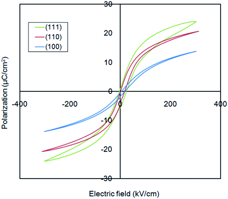 | ||
| Fig. 5 P–E hysteresis loops of the BaTiO3 films in the MDM capacitors. | ||
The DC resistivity of thin films prepared from a variety of film orientations measured at 300 kV cm−1 is shown in Table S3.† The resistivity of BaTiO3(100) film, BaTiO3(110) film, and BaTiO3(111) film were 5.91 × 10⁸ Ω cm, 4.48 × 10⁸ Ω cm, 8.70 × 10⁷ Ω cm, respectively. The BaTiO3(111) film possesses lower resistivity compared with the resistivity of the BaTiO3(100) film. This decreased resistivity has caused the P–E loop to look inflated and not have nicely pinched ends, increasing the values for coercive field and remnant polarization.
We assume that tensile stress in the plane of the growth direction that was induced during the twinned growth of BaTiO3(111) enhanced the ferroelectric properties of the and lowered resistivity compared with the ferroelectric properties of the (100)-oriented BaTiO3 film.
Conclusions
The (100)-, (110)-, and (111)-oriented BaTiO3 films were successfully synthesized on a Pt-coated MgO substrate by CSD processing. The electric properties of the fabricated BaTiO3 thin films were evaluated and revealed that the ferroelectric properties of the BaTiO3(110) film and BaTiO3(111) film are enhanced compared with the BaTiO3(100) film. The enhancement of the ferroelectric properties is assumed to be induced by tensile stress in the same plane as the growth direction. Furthermore, dielectric constants as high as 2000 with stable temperature-dependent BaTiO3 films were produced by a mass production procedure that will benefit thin-film capacitors in the near future.Acknowledgements
The authors thank Masato Adachi for the X-ray pole figure measurements and Tomonori Muraki for the TEM measurement.Notes and references
- J. F. Scott, Science, 2007, 315, 954–959 CrossRef CAS PubMed.
- K.-H. Chen, Y.-C. Chen, Z.-S. Chen, C.-F. Yang and T.-C. Chang, Appl. Phys. A, 2007, 89, 533–536 CrossRef CAS.
- Y. Takeshima, K. Shiratsuyu, H. Takagi and Y. Sakabe, Jpn. J. Appl. Phys., 1997, 36, 5870–5873 CrossRef CAS.
- Z. Liu, P.-T. Lin, W. B. Wessels, F. Yi and S.-T. Ho, Appl. Phys. Lett., 2007, 90, 201104 CrossRef.
- V. S. Dharmadhikari and W. W. Grannemann, J. Appl. Phys., 1982, 53, 8988–8992 CrossRef CAS.
- J. H. Kim and S. Hishita, J. Mater. Sci., 1995, 30, 4645–4650 CrossRef CAS.
- S. Canulescu, G. Dinescu, G. Epurescu, D. G. Mateia, C. Grigoriua, F. Craciunb, P. Verardib and M. Dinescu, Mater. Sci. Eng., B, 2004, 109(1), 160–166 CrossRef.
- G. M. Norton, K. P. B. Cracknell and B. C. Carter, J. Am. Ceram. Soc., 1992, 75, 1999–2002 CrossRef.
- G. M. Norton, C. Scarfone, J. Li, B. C. Carter and W. J. Mayer, J. Mater. Res., 1991, 6, 2022–2025 CrossRef.
- T. Chiba, K. Itoh and O. Matsumoto, Thin Solid Films, 1997, 300(1), 6–10 CrossRef CAS.
- G. M. Norton and B. C. Carter, J. Mater. Res., 1990, 5, 2762–2765 CrossRef.
- C. S. Chern, J. Zhao, L. Luo, P. Lu, Y. Q. Li, P. Norris, B. Kear, F. Cosandey, C. J. Maggiore, B. Gallois and B. J. Wilkens, Appl. Phys. Lett., 1992, 60, 1144 CrossRef CAS.
- D. L. Kaiser, M. D. Vaudin, L. D. Rotter, Z. L. Wang, J. P. Cline, C. S. Hwang, P. B. Marinenko and J. G. Gillen, Appl. Phys. Lett., 1995, 66, 2801–2803 CrossRef CAS.
- Y. S. Yoon, M. N. Kang, H. S. Shin, S. S. Yom, T. W. Kim, J. Y. Lee, D. J. Choi and S.-S. Baek, J. Appl. Phys., 1993, 73, 1547 CrossRef CAS.
- U. Hasenkox, S. Hoffmann and R. Waser, J. Sol-Gel Sci. Technol., 1998, 12, 67–79 CrossRef CAS.
- R. Roy, Science, 1987, 238, 1664–1669 CAS.
- H. Liu, P. Yang, Z. Fan, A. Kumar, K. Yao, K. P. Ong, K. Zeng and J. Wang, Phys. Rev. B, 2013, 87, 220101 CrossRef.
- K. Iijima, T. Terashima, Y. Bando, K. Kamigai and H. Terauchi, J. Appl. Phys., 1992, 72, 2840–2845 CrossRef CAS.
- H. Tabata, H. Tanaka and T. Kawai, Appl. Phys. Lett., 1994, 65, 1970–1972 CrossRef CAS.
- T. Tsurumi, T. Suzuki, M. Yamane and M. Daimon, Jpn. J. Appl. Phys., 1994, 33(1), 5192–5195 CrossRef CAS.
- T. Shimizu, D. Suwama, H. Taniguchi, T. Taniyama and M. Itoh, Appl. Phys. Express, 2013, 6, 015803 CrossRef.
- K. J. Choi, M. Biegalski, Y. L. Li, A. Sharan, J. Schubert, R. Uecker, P. Reiche, Y. B. Chen, X. Q. Pan, V. Gopalan, L.-Q. Chen, D. G. Schlom and C. B. Eom, Science, 2004, 306, 1005–1009 CrossRef CAS PubMed.
- T. Hosokura, N. Iwaji, T. Nakagawa, A. Ando, H. Takagi, Y. Sakabe and K. Hirao, Cryst. Growth Des., 2011, 11(10), 4253–4256 CAS.
- Z. Gui, S. Prosandeev and L. Bellaich, Phys. Rev. B, 2011, 84, 214112 CrossRef.
- T. Schneller and R. Waser, Ferroelectrics, 2002, 267, 293–301 CrossRef CAS.
- F. F. Lange, Science, 1996, 273, 903–909 CAS.
- T. Hosokura, A. Ando and Y. Sakabe, Key Eng. Mater., 2006, 320, 81–84 CrossRef CAS.
- C. L. Jia, K. Urban, S. Hoffmann and R. Waser, J. Mater. Res., 1998, 13, 2206–2217 CrossRef CAS.
- W. R. Schwartz, Chem. Mater., 1997, 9, 2325–2340 CrossRef.
- W. R. Schwartz, P. G. Clem, A. J. Voigt, R. E. Byhoff, V. M. Stry, J. T. Headley and A. N. Missert, J. Am. Ceram. Soc., 1999, 82(9), 2359–2367 CrossRef.
- J. J. Wang, F. Y. Meng, X. Q. Ma, M. X. Xu and L. Q. Chen, J. Appl. Phys., 2010, 108, 034107 CrossRef.
- D. Berlincort and H. Japeze, Phys. Rev., 1985, 111, 143–148 Search PubMed.
- T. Hosokura, K. Kageyama, H. Takagi and Y. Sakabe, J. Am. Ceram. Soc., 2009, 92(1), 253–255 CrossRef CAS.
- H. Oppolzer and H. Schmelz, J. Am. Ceram. Soc., 1983, 66(6), 444–446 CrossRef CAS.
- M. G. Harwood, P. Popper and D. F. Rushman, Nature, 1947, 160, 58–59 CrossRef CAS.
Footnote |
| † Electronic supplementary information (ESI) available: Fig. S1 cross-sectional FE-SEM image of the BaTiO3 films; Fig. S2–S4 cross-sectional TEM images of the BaTiO3 films; Table S1 elastic constants and tensile stress in the plane of the growth direction of (100)-, (110)-, and (111)-oriented film. Table S2 the capacitance of the obtained BaTiO3 films measured at 1 kHz and 0.1 V. Table S3 DC resistivity of thin films prepared from a variety of film orientations measured at 300 kV cm−1. See DOI: 10.1039/c5ra22195a |
| This journal is © The Royal Society of Chemistry 2015 |