
Self-assembled metallic nanoparticle superlattices on large-area graphene thin films: growth and evanescent waveguiding properties†
Tianhao Ouyanga,
Arash Akbari-Sharbafa,
Jaewoo Parka,
Reg Baulda,
Michael G. Cottamab and
Giovanni Fanchini*abc
aDepartment of Physics and Astronomy, University of Western Ontario, 1151 Richmond St, London, Ontario N6A 3K7, Canada. E-mail: gfanchin@uwo.ca; Fax: +1-519-661-2033; Tel: +1-519-661-2111 ext. 86238
bCentre for Advanced Materials and Biomaterials Research (CAMBR), University of Western Ontario, 1151 Richmond St, London, ON N6A 5B7, Canada
cDepartment of Chemistry, University of Western Ontario, 1151 Richmond St, London, ON N6A 5B7, Canada
First published on 10th November 2015
Abstract
We report a facile fabrication method for copper nanoparticle superlattices, based on thermal evaporation of ultrathin layers of copper on solution-processed thin films formed by few-layer graphene platelets. We show that the annealing of these systems in nitrogen without previous exposure to air prompts the heterogeneous nucleation of the Cu layer into nanoparticle superlattices self-assembled along specific crystallographic directions of graphene. Theoretical calculations suggest a lowest formation energy for Cu-nanoparticle arrays aligning along armchair directions, indicating that their self-assembly is energetically more favourable. The possibility of using these superlattices in evanescent waveguiding devices is explored by three-dimensional scanning near-field optical microscopy. The light-confining properties of our systems in the near-field indicate that our nanoparticle superlattices are poised to satisfy the technological demands required by nanophotonics devices.
1. Introduction
Solution-processed, graphene-based thin films formed by assemblies of single-layer and multi-layer graphene platelets may offer unique means to translate engineered graphene-based materials from the realm of fundamental research into practical applications in transparent and flexible electronics1–3 in a more cost-effective way than chemical-vapour deposited graphene.4 Solution-prepared graphene thin films decorated with random distributions of metallic nanoparticles to enhance their optical and electronic properties have already shown promise in specific applications,5,6 and new devices would emerge through self-assembling these nano-metallic phases into superlattices. Attempts to decorate two-dimensional (2D) materials with metallic nanoparticles can be traced back over several years,7–9 but the spontaneous formation of superlattices of metallic nanoparticles on graphene-based materials on a generic substrate has not yet been reported.Although disordered assemblies of size-selective Au particles on graphene were presented by Luo et al.,10 no periodic superlattices could be achieved by these authors. It is only recently that calculations by Zhou et al.11 have suggested the possibility of self-assembling periodic arrays of alkali atom clusters along specific lattice direction of graphene, but, so far, these architectures have not been experimentally obtained. Superlattices of larger metal nanoparticles have been neither previously predicted nor experimentally produced, to the best of our knowledge.
Regarding interfaces with graphene, two different classes of metals have been identified:12 a few elements (e.g. Co, Ni, and Pd) form relatively strong chemical bonds with graphene, while others (e.g. Cu and Au), for which adhesion relies on weaker van der Waals interactions, seem to offer better opportunities for self-assembly and nano-manipulation. To date, expensive techniques normally suitable only over small areas are required to attain nanopatterned structures on graphene or other 2D materials.13 These “bottom-up” approaches include nanolithography and nano-contact printing.
Here we will report for the first time the spontaneous assembly of superlattices of Cu nanoparticles (Cu-np's) on single-layer to few-layer graphene thin films. These superlattices are obtained by a process consisting in the annealing at moderate temperatures (250–400 °C) of a thin copper layer that had not been previously exposed to air. This process is cost-effective, scalable and is suitable for extensions to nanoparticles of other metals that weakly bond to graphene9 or to produce nanoparticle arrays on other 2D materials.
The diameter of our self-assembled Cu-np's and their superlattice inter-particle spacing are usually less than 10–20 nm, while the superlattice interline spacings are roughly one order of magnitude larger, comparable to the wavelength of visible light. As graphene offers an excellent platform for nanophotonics,14,15 our graphene-based metal nanoparticle superlattices are uniquely positioned to be used in light-confining evanescent devices.16 In this work, the evanescent waveguiding properties of our systems will be explored and the ability of graphene-based Cu-np's superlattices to channel near-field electromagnetic radiation will be explored. To this end, a three-dimensional scanning near-field optical microscope (3D-SNOM) previously developed by Ezugwu et al.17 will be used to characterize our samples and extract the electric field intensity perpendicular to the air–superlattice interface at heights Z = 0−1200 nm. The potential of our system to act as a near-field waveguide will be discussed and 3D-SNOM images, showing confinement of green light within 500 nm above the sample surface, will be presented.
2. Results and discussion
2.1 Sample preparation
Graphene-based thin films used in our study were deposited by a method previously developed by Eda et al.18 for graphene oxide laminates, and extended by Sharifi et al.19 to non-oxidized graphene thin films by using surfactant-assisted exfoliation of graphite. This method produces large amounts of suspensions of single and few-layer graphene in water.19 The as-obtained aqueous dispersions of graphene were vacuum filtrated onto porous sacrificial membranes using a technique originally devised by Wu et al.20 for carbon nanotubes. These membranes can be used to transfer graphene thin films onto different substrates over large-areas, as demonstrated in panel a of Fig. 1. The possibility to use solution-processed graphene thin films for our self-assembly experiments anticipates that our superlattice fabrication method is highly tolerant to impurities and relatively insensitive to the number of graphene layers. A typical scanning electron micrograph (SEM) of a bare graphene-based thin film is shown in panel b of Fig. 1.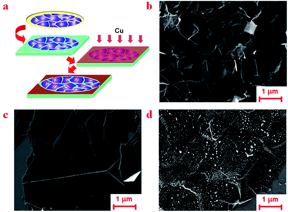 | ||
| Fig. 1 (a) Fabrication of Cu-np's superlattices: (i) deposition of a large-area graphene thin film on Si(100) from a sacrificial filter membrane previously loaded with graphene by vacuum filtration, (ii) thermal evaporation of a 0.7 ± 0.3 nm-thick Cu layer on top of the film, and (iii) thermal annealing of the system with the formation of periodic arrays of Cu-np's. (b) Scanning electron micrograph (SEM) of a bare graphene-based thin film on Si(100), (c) SEM of the same film after thermal evaporation of the Cu layer, and (d) SEM thermal annealing of the graphene/Cu film with the subsequent rearrangement of Cu into self-assembled superlattices of Cu-np's. | ||
Cu-np's were formed on our graphene-based thin films by thermally-induced nucleation from a flat metallic Cu thin film. Similar to the mechanism of dewetting,21 this a process that combines surface and interface energy minimization22 at conditions depending on the annealing temperature and time, film thickness, and substrate wettability by the metal layer. The thickness of the thermally evaporated Cu layer was kept constant at 0.7 ± 0.3 nm (Fig. 1, panel c) for all of the experiments described here. At this nanoscale thickness, a Cu layer is reported to melt below 200 °C (ref. 23 and 24) and a set of samples annealed at different temperatures above the melting point of the Cu film were produced. The superlattice reported in Fig. 1, panel d is indicative of a typical annealing result at 360 °C, showing the nucleation of Cu-np's on each graphene flake into a superlattice with high degree of ordering. While nanoparticles shown in Fig. 1d are typically less than 20 nm in diameter, a few randomly assembled Cu-np's, larger and less spherical, can also be noticed on some of the graphene flakes in this image. This is an effect we assign to Ostwald ripening:22 kinetic effects, more important at higher temperatures, displace the nanoparticles, induce collisions and lead larger and less spherical objects (∼50–100 nm) to grow at the expenses of the smaller and periodically arranged Cu-np's. This is an undesired disordering phenomenon and careful optimization of the annealing time and temperature is required to mitigate and prevent it.
Fig. 2 demonstrates the role of temperature in the formation of superlattices of Cu-np's. It can be observed that, at the lowest annealing temperature (200 °C, panel a), formation of ordered structures is rare, except in the proximity of graphene flake edges. Copper nucleation is typically very limited at such temperatures23,24 and produces semi-continuous films of interconnected nano-structures. The ideal annealing temperature appears to be higher, about 360 °C, at which ordered superlattices of Cu-np's at 18 ± 4 nm diameter can be found. At 360 °C and 8 h (Fig. 2, panel b) Cu-np's align well along lines parallel to the armchair direction of the graphene lattice, with relatively low (Δx = 12 ± 3 nm) inter-particle spacing, while the spacing between lines (Δy = 182 ± 6 nm) is significantly higher. At higher temperatures (Fig. 2, panel c) Ostwald ripening occurs, mostly from particles that become displaced from their preferential superlattice sites due to kinetic effects. We suspect that, even at the lowest annealing temperatures, nucleation of Cu-np's mostly occurs when the Cu thin layer is in the molten state, since the melting temperature of metallic nanoparticles and ultrathin metallic films of only a few atomic layers is significantly lower than in the corresponding bulk metal.22 When the characteristic size of the ripening particles becomes large enough to solidify them at that specific annealing temperature, the nucleation process ends, resulting in their random distribution over relatively large area.
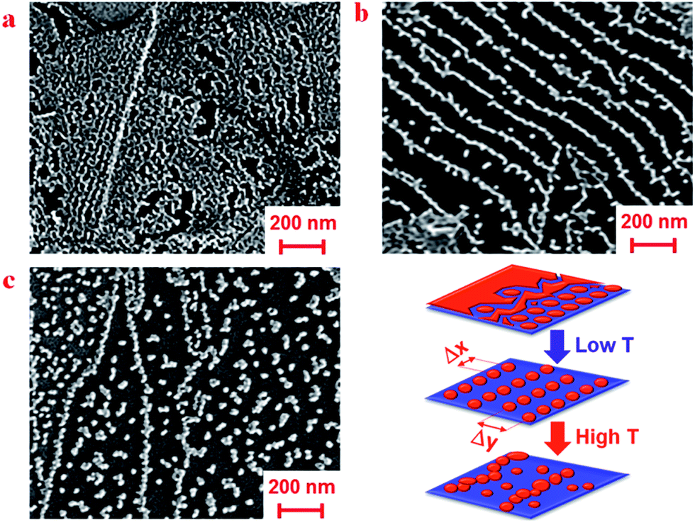 | ||
| Fig. 2 SEM images of samples annealed for 8 h at increasing temperatures: (a) 200 °C (b) 360 °C, with Δx = 12 ± 3 nm and Δy = 182 ± 6 nm, and (c) 440 °C. A diagram (d) illustrating the different behaviour of Cu-np's nucleated at different temperatures is also provided, showing a trend from semi-continuous and nano-structured Cu layers at the lowest temperatures to sparse assemblies at the highest temperatures, with superlattices forming at intermediate temperatures. | ||
Fig. 3 explores the role of annealing time in the formation of superlattices. Constant interline spacings Δy are established at relatively short annealing times (5 h, panel a), but significant imperfections in the superlattices are due to the fact that, not infrequently, arrays of Cu-np's are actually parallel curved lines if too short annealing times are used. At the optimal annealing time of about 8 h, superlattices with uniformly distributed and remarkably straight lines of Cu-np's are formed, with an interline lattice spacing Δy = 186 ± 6 nm at 360 °C, as shown in Fig. 3b. At longer times (e.g. at 12 h at 360 °C), the progressive coalescence of nearest-neighbouring lines of Cu-np's becomes the dominant process. Consequently, exceedingly long annealing times result in graphene platelets relatively free of Cu-np's, with many isolated lines of Cu-np's tending to converge into one, as shown in panel c of Fig. 3. Relatively small fluctuations of the annealing temperatures and times about 360 °C and 8 h lead to the possibility to design superlattices with different lattice parameters, Δx and Δy, as described in the ESI.†
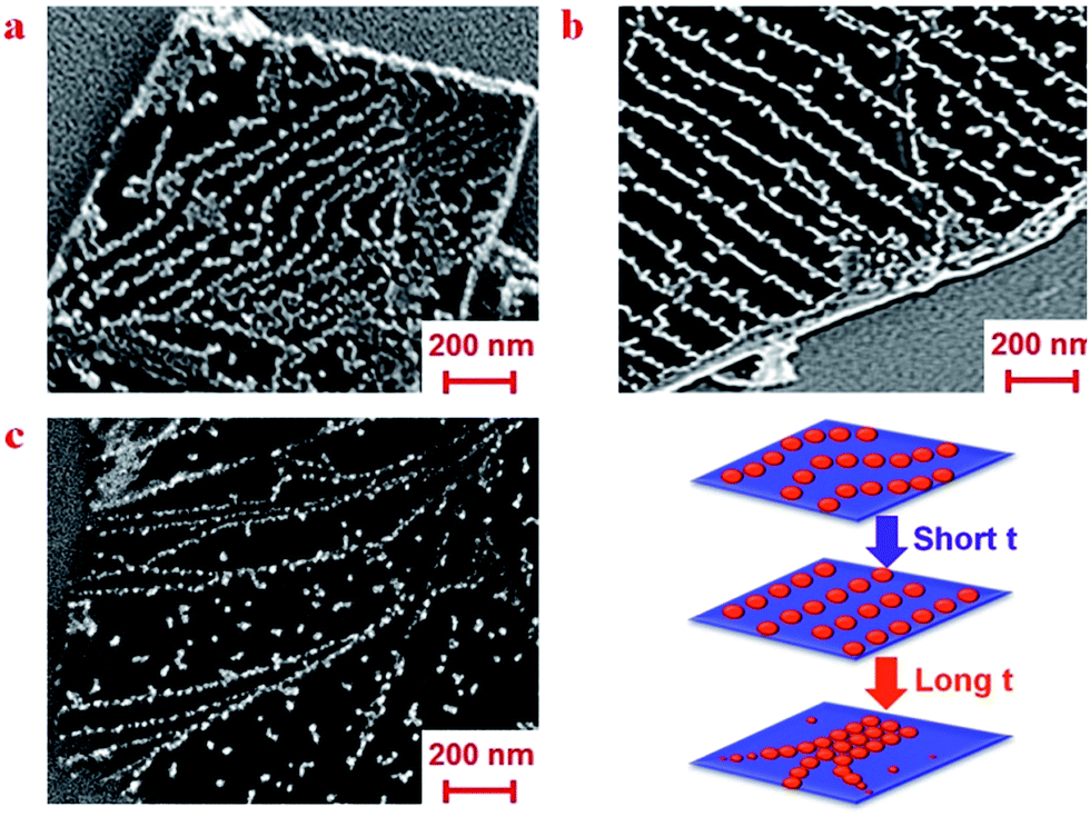 | ||
| Fig. 3 SEM images taken from samples annealed at 360 °C at different times (a) 5 h (b) 8 h, with Δy = 186 ± 6 nm (c) 12 h. (d) Diagram illustrating the different behaviour of Cu-np's self-assembled at different times is also provided, showing a trend from curved lines of Cu-np's at relatively constant distances Δy at the shortest times to isolated and coalescing lines of Cu-np's at the longest times, with superlattices forming at intermediate times. | ||
2.2 Theoretical growth model
Understanding why arrays of Cu atoms aligned with armchair directions are energetically favoured over other arrangements is essential for modelling the formation of Cu-np's superlattices in terms of the subsequent nucleation of each one of these atomic arrays into a line of metallic particles. We adopted a Cu![[thin space (1/6-em)]](https://www.rsc.org/images/entities/char_2009.gif) :C area ratio of 1:8, consistent with a uniform 0.7 nm layer of Cu, to perform calculations based on a numerical model (see experimental details) which assumes modified tight-binding parameters consistent with the results of Zhou et al.11 for arrays of alkali atoms. Quantification of the formation energies for uniform distributions and arrays of Cu atoms along either the armchair or zigzag direction of graphene (Fig. 4a) suggests that armchair arrays are the most energetically favourable configuration. This is also confirmed by the fact that, at the longest annealing times, when multiple lines of Cu-np's tend to coalesce (Fig. 4b), they are typically parallel to an armchair edge and intersect at an angle of 120°.
:C area ratio of 1:8, consistent with a uniform 0.7 nm layer of Cu, to perform calculations based on a numerical model (see experimental details) which assumes modified tight-binding parameters consistent with the results of Zhou et al.11 for arrays of alkali atoms. Quantification of the formation energies for uniform distributions and arrays of Cu atoms along either the armchair or zigzag direction of graphene (Fig. 4a) suggests that armchair arrays are the most energetically favourable configuration. This is also confirmed by the fact that, at the longest annealing times, when multiple lines of Cu-np's tend to coalesce (Fig. 4b), they are typically parallel to an armchair edge and intersect at an angle of 120°.
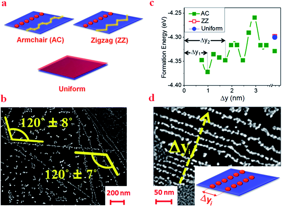 | ||
| Fig. 4 (a) Simulations of single arrays of Cu along armchair (AC) and zigzag (ZZ) directions of a graphene lattice as well as for a uniform copper distribution with Cu:C = 1:8. (b) SEM image at 500 °C annealing temperature showing Cu-np's lines along armchair edges of graphene domains. (c) Theoretical formation energies of individual Cu-np's lines along armchair (AC) and zigzag (ZZ) directions and parallel lines of Cu-np's at interline distance Δy along AC directions. Minima for specific values of {Δyi} can be observed (with Δy1 = 1.0 nm and Δy1 = 1.7 nm evidenced in the plot). Each minimum corresponds to a favourable interline distance for the formation of superlattices. (d) Special case in the proximity of an armchair graphene edge, in which an irregular superlattice with multiple values of {Δyi} for parallel Cu-np's lines is shown. | ||
The interline periodicity of our superlattices (Fig. 4c) could also be theoretically inferred by calculating the formation energies of parallel arrays of Cu atoms as a function of their inter-array distance Δy. We find that the formation energy of parallel Cu-atom arrays depends periodically on Δy and exhibits a sequence of minima {Δyi} corresponding to preferred distances at which Cu-np's lines tend to form. In special cases (Fig. 4d) we could also observe a gradient in the interline spacing, with a sequence of increasingly large values of Δy = Δyi separating neighbouring lines. This qualitatively explains the growth mechanism of Cu-np's superlattices in two steps: in the first step, a relatively uniform Cu layer resulting from thermal evaporation divides in parallel arrays of Cu atoms so that the interface energy of the structure reaches a local minimum and spacing in the y-direction is established. In the second step, each array of Cu-atoms nucleates into a line of weakly spaced Cu-np's and a constant spacing Δx is established in the x-direction.
2.3 Evanescent waveguiding properties
In order to investigate the ability of our superlattices to sustain the propagation of evanescent waves confined in the proximity of the graphene surface and propagating along the direction parallel to the lines of Cu-np's, 3D-SNOM experiments were carried out in reflection-collection mode as demonstrated in Fig. 5a and b.17 In these experiments, a 532 nm laser is launched into a single-mode optical fiber and the superlattice samples are positioned with Cu-np lines parallel to the X-axis of the microscope shown in Fig. 5a. An SMA beam collimator attached to the fiber ending is used to match the laser source with the superlattice and focus the light parallel to the sample surface and the Cu-np lines, at a height in the correspondence of the tiny gap between the surface and an aperture-type atomic force microscopy (AFM)-SNOM cantilever. The AFM-SNOM tip ends with a 50 nm aperture nanofabricated using focused ion beam (FIB) milling, which is specifically designed to emit and collect light in the near-field. Thus, modes generated by the laser source, which are evanescent in Z-direction and propagating along the sample surface, can be locally collected at any (X, Y, Z) location by the AFM-SNOM tip aperture, on which an upright confocal microscope is focused. The confocal microscope is fiber-coupled to a photomultiplier for quantifying the light intensity collected by the tip at point (X, Y, Z).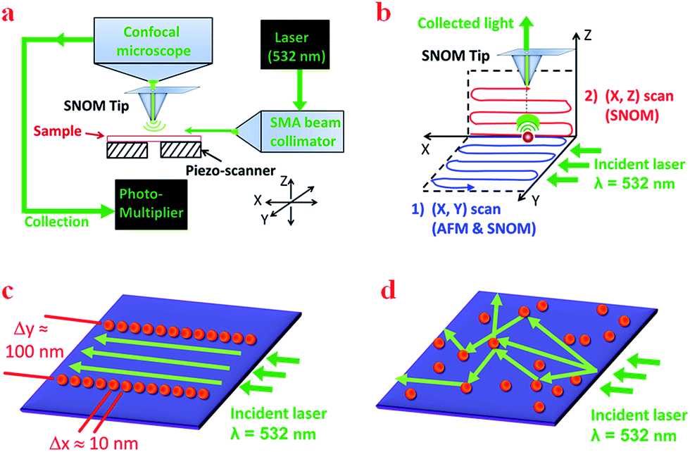 | ||
| Fig. 5 (a) Schematic of Witec Alpha 300S microscope modified for reflection-collection 3D-SNOM imaging. (b) Diagram of the 3D-SNOM configuration used for measurements of topography and light scattering from Cu-np superlattices. Collection-mode and topography images are simultaneously obtained from an (X, Y) AFM/SNOM scan at Z = 0, while (X, Z) SNOM cross-section scans at selected regions enabled us to obtain the position of light scattered by the nanoparticles at different heights from the sample surface. Schematic of Mie scattering in different systems of Cu-np's: (c) coherent scattering in superlattices and (d) incoherent scattering combined with light absorption in randomly distributed Cu-np's. | ||
First, during each 3D-SNOM measurement, a contact-mode AFM-SNOM scan is performed and the distribution of the intensity of near-field within the (X, Y) plane is probed in the close proximity of the surface, as shown in Fig. 5b, step (1). This measurement provides an AFM scan of the sample surface in conjunction with the (X, Y) SNOM scan at Z = 0. Reproducible tip position relative to the sample is obtained with an (X, Y) piezo-scanner and a controlling feedback loop. In a second measurement step (step 2 in Fig. 5b), an (X, Z) SNOM scan is carried out at increasing Z by selecting a specific cross section X, obtained from the (X, Y) image. In order to perform this operation, the distance Z between the tip and the sample surface is increased using a second piezo-scanner, operating in the (X, Z) plane, with Z = 0 to be set at the point at which the tip is in contact with the sample. This procedure enables us to study the scattered waves and their propagation at different vertical positions and is repeated at decreasing tip-sample distance until contact with the surface is restored, in order to ensure Z-axis reproducibility.
SNOM (X, Z) scans were specifically used in our study for probing the decay of near-field evanescent modes away from the sample surface. Vertically, evanescent fields only exist within about one wavelength of incident light. In the near field, scattering dominates the interaction between light and our superlattices, as Cu-np's are known to display strong Mie scattering at λ = 532 nm.25,26 Parallel Cu-np's lines with interline distances (Δy ∼ 102 nm) of the same order of magnitude as the incident wavelength provide a preferential direction for Mie scattering.26 Light is only absorbed transversally to Cu-np's lines, leaving only scattering with little attenuation for longitudinal modes, hence an evanescent wave can be confined (Fig. 5c). Conversely, light will be isotropically scattered in all directions by randomly distributed Cu-np's (Fig. 5d) causing interference between far-field modes along Z.
Based on these considerations, a demonstration of evanescent waveguiding in Cu-np's superlattices, as opposed to isotropic Mie scattering in regions of non-aligned Cu-np's, is offered in Fig. 6. The region in the AFM topography image in Fig. 6a corresponds to the reflection-collection mode SNOM image shown in Fig. 6b, in which a brighter pixel represents a higher intensity of scattered light being collected at that point in close proximity of the sample. Since AFM is not capable of resolving our superlattices, we obtained a SEM image of the same location (Fig. 6c) using lithographically patterned sample markers. It clearly shows that a superlattice with lines of Cu-np's parallel to the light propagation direction (which is vertical, along the Y-axis, in Fig. 6a–c) exists at section A–A′. Conversely, SEM shows that Cu-np's distribution is less ordered, and not parallel to the light propagation direction, in the sample cross section labelled as B–B′ in Fig. 6a–c. Consequently, an (Y, Z) scan along section A–A′ is expected to demonstrate evanescent waveguiding properties, while a similar scan along section B–B′ is expected to exhibit a sequence of constructive and destructive interference patterns along the Z-axis as a consequence of incoherent Mie scattering.25,26 Fig. 6d presents vertical SNOM scans in Z-direction for the two sections, A–A′ and B–B′. Section A–A′ represents an area that, in panel b, is significantly brighter than the surrounding regions, meaning that more light was collected from that area. This is an indication of strong light confinement, since parallel lines of Cu-np's promote coherent Mie scattering with little light absorption from Cu-np's that offer a very low cross-section to the incident wave.
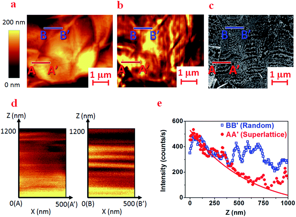 | ||
| Fig. 6 (a) Typical AFM and (b) reflection-collection SNOM images obtained simultaneously from one of our Cu-np's superlattices annealed at 360 °C for 8 h (c) SEM micrograph, obtained using lithographically patterned markers from the same sample region as in panels a and b. (d) Vertical SNOM scans in Z-direction for cross-sections indicated as A–A′ (left) and B–B′ (right) in panels a–c. The Z-axis extends from 0 to 1200 nm in this figure. (e) Scans in panel d show an exponential decay of the evanescent wave mode at a distance Z from the surface for section A–A′ (corresponding to a periodic superlattice). Conversely, they show random interference patterns for section B–B′ (corresponding to a random distribution of Cu-np's). The red solid line is a fit that demonstrates the exponential decay of the evanescent mode in section A–A′. | ||
Integrated light intensity profiles extracted from Fig. 6d are reported in panel e of Fig. 6 as a function of Z. For section A–A′, corresponding to ordered Cu-np's superlattices, an exponential decay of light intensity in the proximity of the sample can be observed, as witnessed by the analytical exponential fit demonstrated in panel e for the integrated attenuation in the A–A′ cross section. Conversely, the light intensity profile for section B–B′, characterized by randomly oriented Cu-np's, undergoes multiple oscillations due to the superposition of multiple and incoherent Mie scatterings in arbitrary directions. Typically, a maximum of the interference pattern at Zmax ≈ λ can be predicted, with the first minimum at values of Z slightly higher than Zmin ≈ λ/2.25 These predictions compare very well of our experiments, for which we can observe, Zmax ≈ 530 nm and Zmin ≈ 380 nm from the blue trace in Fig. 6e, corresponding to the BB′ section in Fig. 6a–c. Oscillating light intensity profiles of this type are relatively rare in our system and are confined to disordered areas, which points at the robustness of the evanescent waveguiding properties of Cu-np's superlattices.
The evanescent waveguiding properties of our superlattices are demonstrated by the (X, Z) SNOM scan at the left side of Fig. 6d, corresponding to section A–A′. Along such section, confinement of the electromagnetic radiation in the bright yellow zone in the proximity of the sample surface can be observed. There is a strong attenuation of light intensity at values of Z within a few tens nm from the sample surface, which corresponds to evanescent modes. Conversely, the (X, Z) SNOM scan along section B–B′ of Fig. 6a–c is presented on the panel at the right side of Fig. 6d and reveals a dark region in the proximity of the sample surface, with subsequent maxima and minima of scattered light intensity, due to constructive and destructive interference of incoherent far-field modes. This is typical of relatively rare regions of our samples in which Cu-np's are disorderly distributed. The same behavior was previously observed in random arrangements of metal nanoparticles on glass.17
In our evanescent waveguides corresponding to ordered regions in our samples (e.g. sect. A–A′ in Fig. 6) the role of graphene layers is to determine the polarisation of the propagating radiation. Graphene is an optically anisotropic medium with a high in-plane imaginary part of the dielectric constant (ε∥ = ε′∥ + iε′′∥ ≈ 6 + i7 at λ = 532 nm) while the out-of-plane imaginary part is nearly zero (i.e. ε⊥ = ε′⊥ ≈ 3 at λ = 532 nm).27 Unpolarised light entering graphene at grazing incidence angles (see Fig. 5b and c) will be strongly attenuated in its in-plane polarisation component, while only the component polarized in out-of-plane direction will propagate along the graphene surface. The role of the Cu-np superlattice in our waveguides is to offer a preferential direction for light propagation on graphene along the X-axis, corresponding to the direction of parallel lines of Cu-np's. With this architecture, the decay of the electric field along the Z-axis is determined by the interline distance between Cu-np lines. We thus expect a decay constant of the same order of magnitude of Δy, which is of the order of magnitude of 102 nm in our case, as experimentally observed in Fig. 5e. Conversely, if propagation occurred with plasmonic waveguide modes, via adjacent nanoparticles within each line, we suspect that the decay constant would be significantly lower, of the order of magnitude of the Cu-np diameter, but the evancescent field intensity would also be significantly lower, due to the lower cross-section area of the waveguiding medium. However, more experiments are required to substantiate this hypothesis.
Perhaps, the closest far-field counterparts of our near-field waveguideing superlattices are coplanar waveguides28 consisting of parallel conducting strips of metal, equivalent to our Cu-np lines, assembled on a dielectric substrate grown on a grounded base, equivalent to our graphene thin film on silicon. Like coplanar waveguides, our waveguiding superlattices are most likely not supporting true transverse electromagnetic (TEM) modes because magnetic fields may have significant longitudinal components along the Cu-np lines and electric fields may have important longitudinal components at the graphene–silicon interface. Our evancescent waveguiding properties are likely of the hybrid mode, even though some similarities with TEM00 modes are certainly present.
3. Conclusions
We demonstrated that solution-processed graphene thin films offer a unique platform for the formation of copper nanoparticle superlattices, with parallel lines of Cu-np's that preferentially self-assemble along the armchair crystallographic direction of graphene. An essential component of our superlattice fabrication process is the deposition of ultrathin Cu layers by thermal evaporation and their subsequent annealing and manipulation in inert atmosphere (e.g. nitrogen) without intermediate exposure to air. Our theoretical calculations suggest that Cu-np's arrays tend to form due to the combined minimization of surface and interface energies between graphene and the overlying metal system. At the optimal formation conditions for these superlattices, which correspond to approximately 360 °C and 8 h annealing time, superlattices are formed by lines of weakly spaced (Δx ∼ 101 nm) Cu-np's with significantly larger (Δy ∼ 102 nm) interline spacings. These values of Δy, of the same order of magnitude of the wavelengths of visible light, suggested that our systems possess evanescent waveguiding properties for light propagating parallel to the Cu-np's lines. We have demonstrated waveguiding properties using three-dimensional scanning near-field optical microscopy, which indicates that our Cu-np's superlattices on graphene are potentially suitable for the fabrication of nanophotonic waveguiding devices.Not only is our superlattice fabrication method suitable to produce Cu-np arrays, but is general enough to be used with a large variety of other metals that weakly bond to graphene (e.g. Au).29 Other future applications of our work may stem from the extension of this fabrication method to additional three-dimensional materials different from graphene, as well as the additional optimization of the growth conditions and the fine-adjustment of the superlattices parameters. Such future work may broaden the applications of self-assembled metallic superlattices on two-dimensional thin films of graphene and other materials in light trapping devices, magnonic crystals, plasmonic enhancers, and others.30
4. Methods
Graphene-based thin films were fabricated using the method developed by Sharifi et al. and extensively discussed in ref. 19. Nanocrystalline graphite (Sigma-Aldrich, CAS 7782-42-5) was exfoliated in water using RNA as a surfactant for stabilizing single-layer and few-layer graphene flakes. A volume of 3 ml RNA water solution with graphene flakes suspended in it was filtrated through 0.22 μm pore diameter nitrocellulose membranes (Millipore, HTTP02500) to deposit the graphene flakes, and subsequently to transfer them onto silicon substrates. Afterwards, the filter membrane was left in contact with the substrate and dried under load at 80 °C for 12 h in a box oven. After drying, the nitrocellulose filter membranes were etched with multiple acetone and methanol baths leaving behind a thin graphene-based film on its substrate. For our studies, these graphene-based thin films were deposited onto silicon (100) substrates. Pre-annealing in nitrogen atmosphere, to prevent oxidation from air, was conducted at 500 °C for 3 h to remove RNA from the surface of graphene. It also led to the formation of defects on graphene flakes that were beneficial for metallic nanoparticles to adhere and nucleate at the graphene surface.29 Specific characterization, including Raman, atomic force microscopy (AFM), scanning electron microscopy (SEM) and UV-visible spectrophotometry were used to ascertain that the samples were mainly formed by single-layer and few-layer graphene flakes, as discussed in detail in ref. 19.Cu layers were deposited on graphene-based thin films by a thermal evaporator installed in a vacuum chamber (KJ Lesker, 10−8 mTorr base pressure) attached to a contiguous nitrogen-loaded glove box (Nexus II, Vacuum Atmospheres Inc.) without any intermediate exposure to air. A 99.999% Cu pellet was placed in an alumina crucible heated by a tungsten basked heater using a high-current power supply (Hewlett-Packard HP6466C). Silicon (100) wafers with a graphene thin film on their surface were placed on a turnable square substrate holder approximately 50 cm above the Cu evaporation source. Cu thickness of 0.7 ± 0.3 nm was obtained and monitored using a Sycom STM-2 quartz oscillator-based thickness monitor. For thermal evaporation, the high-current power supply was operated at 8.5 V and 70 A, which offers relatively low (∼0.5 nm min−1) Cu deposition rates. In order to nucleate Cu-np's from the deposited Cu layers, samples were extracted from the vacuum chamber and manipulated in the contiguous glove box, in which samples were annealed in nitrogen on a hot plate. A set of 25 identical graphene thin films that were simultaneously coated with Cu were annealed under conditions that can be described by a 5 × 5 matrix: 5 groups of samples annealed at different temperatures (200 °C, 280 °C, 360 °C, 480 °C and 540 °C), with each group annealed for 5 different times (1 h, 3 h, 5 h, 8 h and 12 h). Other annealing attempts were also conducted individually.
All samples were characterised using a Zeiss LEO 1540XB SEM operated at 1 kV and equipped with an Energy Dispersive X-ray accessory for compositional analysis. Parameters such as the diameters of the Cu-np's, lattice interparticle spacing and lattice interline spacing were estimated by measuring the distances between particles using a specialized software package (ImageJ, Java 1.6.0_20 64-bit).31 SEM-based e-beam lithography was used to apply 1 μm long markers in the proximity of the analysed regions of the superlattices and perform scanning-probe microscopy imaging (AFM and SNOM) on the very same sample regions.
Scanning-probe images were recorded using a Witec Alpha 300S aperture-type SNOM system integrated on an AFM microscope and specifically modified for 3D-SNOM.17 AFM and SNOM images are acquired simultaneously with this setup. Reflection-collection SNOM was used for our evanescent waveguiding characterization experiments. A 50 mW, 532 nm, solid state laser (Excelsior, Spectra Physics) is directed to illuminate the sample horizontally and light scattered at the sample surface is collected from the 80 nm-diameter aperture of a hollow AFM-SNOM tip (SNOM-C, NT-MDT Co.) mounted below a high-resolution confocal microscope focused at the tip apex. Light collected by the confocal microscope is subsequently channeled into an optical fiber connected to a photomultiplier tube (U-68000, Hamamatsu) operating in photon-counting mode. An (X, Y) scan was firstly recorded at the sample surface, corresponding to Z = 0. Then, (X, Z) SNOM scans were recorded on selected cross sections at Y = const. to obtain relevant information about the amount of light scattered by the particles at different heights above the sample surface. Careful positioning of the sample along the Z-axis was made using a piezo-scanner and a stepper motor operating in Z-direction, to ensure the maximization of the amount of light coming from the SMA coupler at Z = 0 and in order to generate accurate (X, Z) SNOM scans. Fine adjustment was also made by rotating the sample using the piezo-scanner operating in (X, Y) direction, in order to position the laser beam exiting from the SMA coupler and achieve an incident light propagation direction parallel to the interparticle spacing, Δx, which maximizes the coupling with the superlattice samples.
For theoretical calculations, we employed a tight-binding model to deduce the electronic band structure and the formation energy of graphene decorated with Cu atoms.32 The electronic wave functions of metallic atoms absorbed on graphene show modification of π-bonds in the immediate vicinity of the metallic atoms without altering the bond structure of graphene or producing any significant lattice distortions.32 Thus, we could model the effect of the interaction of Cu atoms with C atoms of graphene in second quantization at the tight-binding level, by modifying the interaction energy of π-electron bonds for lattice sites in the immediate vicinity of Cu atoms as discussed in detail in ref. 32. Affected C![[double bond, length as m-dash]](https://www.rsc.org/images/entities/char_e001.gif) C bonds are expected to have an increased interaction energy since metallic atoms absorbed on graphene transfer a net negative charge to graphene, increasing the bond energy of π-electron influenced by the metallic atoms. Various distributions of metallic atoms absorbed on graphene were considered by defining the particle locations for each distribution (see further details of this model in the ESI†).
C bonds are expected to have an increased interaction energy since metallic atoms absorbed on graphene transfer a net negative charge to graphene, increasing the bond energy of π-electron influenced by the metallic atoms. Various distributions of metallic atoms absorbed on graphene were considered by defining the particle locations for each distribution (see further details of this model in the ESI†).
Acknowledgements
GF acknowledges a Canada Research Chair in carbon-based nanomaterials and nano-optoelectronics, financial support from the Canada Foundation for Innovation and an Early Researcher Award from the Ontario Ministry of Research and Innovation. GF and MGC acknowledge funding from the Natural Sciences and Engineering Research Council of Canada under the Discovery Grant program. The authors would like to thank Sabastine Ezugwu for contributing to some parts of Fig. 5 and for fruitful discussions on 3D-SNOM. High performance computing time at the Ontario Shared Hierarchical Academic Research Computer Network (SHARCNet) is also gratefully acknowledged. Part of this work was carried out at the Western University Nanofabrication Facility.References
- R. Bauld, F. Sharifi and G. Fanchini, Int. J. Mod. Phys. B, 2012, 26, 1242004 CrossRef.
- O. E. Andersson, B. L. V. Prasad, H. Sato, T. Enoki, Y. Hishiyama, Y. Kaburagi, M. Yoshikawa and S. Bandow, Phys. Rev. B: Condens. Matter Mater. Phys., 1998, 58, 16387 CrossRef CAS.
- A. Milchev, E. Vassileva and V. Kertov, J. Electroanal. Chem. Interfacial Electrochem., 1980, 107, 323 CrossRef CAS.
- A. N. Obraztsov, Nat. Nanotechnol., 2009, 4, 212 CrossRef CAS PubMed.
- Y. Zhang, S. Liu, L. Wang, X. Qin, J. Tian, W. Lu, G. Chang and X. Sun, RSC Adv., 2012, 2, 538 RSC.
- Y. Li, X. Fan, J. Qi, J. Ji, S. Wang, G. Zhang and F. Zhang, Nano Res., 2010, 3, 429 CrossRef CAS.
- R. Muszynski, B. Seger and P. V. Kamat, J. Phys. Chem. C, 2008, 112, 5263 CAS.
- S. Ghosh, I. Calizo, D. Teweldebrhan, E. P. Pokatilov, D. L. Nika, A. A. Balandin, W. Bao, F. Miao and C. N. Lau, Appl. Phys. Lett., 2008, 92, 151911 CrossRef.
- J. K. Lee, K. B. Smith, C. M. Hayner and H. H. Kung, Chem. Commun., 2010, 46, 2025 RSC.
- Z. Luo, L. A. Somers, Y. Dan, T. Ly, N. J. Kybert, E. J. Mele and A. T. C. Johnson, Nano Lett., 2010, 10, 777 CrossRef CAS PubMed.
- J. Zhou, S. Zhang, Q. Wang, Y. Kawazoe and P. Jena, Nanoscale, 2015, 7, 2352 RSC.
- G. Giovannetti, P. A. Khomyakov, G. Brocks, V. M. Karpan, J. van den Brink and P. J. Kelly, Phys. Rev. Lett., 2008, 101, 026803 CrossRef CAS PubMed.
- A. N. Shipway, E. Katz and I. Willner, ChemPhysChem, 2000, 1, 18 CrossRef CAS PubMed.
- A. K. Geim and K. S. Novoselov, Nat. Mater., 2007, 6, 183 CrossRef CAS PubMed.
- A. K. Geim, Science, 2009, 3, 1530 CrossRef PubMed.
- D. Ganic, X. Gan and M. Gu, Optik, 2002, 113, 135 CrossRef.
- S. Ezugwu, H. Ye and G. Fanchini, Nanoscale, 2015, 7, 252 RSC.
- G. Eda, G. Fanchini and M. Chhowalla, Nat. Nanotechnol., 2008, 3, 270 CrossRef CAS PubMed.
- F. Sharifi, R. Bauld, M. S. Ahmed and G. Fanchini, Small, 2012, 8, 699 CrossRef CAS PubMed.
- Z. Wu, Z. Chen, X. Du, J. M. Logan, J. Sippel, M. Nikolou, K. Kamaras, J. R. Reynolds, D. B. Tanner, A. F. Hebard and A. G. Rinzler, Science, 2004, 305, 1273 CrossRef CAS PubMed.
- S. Logothetidis, Nanostructured Materials and Their Applications, Springer Science & Business Media, Heidelberg, 2012 Search PubMed.
- G. Cao, Nanostructures & Nanomaterials: Synthesis, Properties and Applications, Imperial College Press, London, 2004 Search PubMed.
- D. Mott, J. Galkowski, L. Wang, J. Luo and C. J. Zhong, Langmuir, 2007, 23, 5740 CrossRef CAS PubMed.
- A. K. Chawla and R. Chandra, J. Nanopart. Res., 2009, 11, 297 CrossRef CAS.
- C. F. Bohren and D. R. Huffman, Absorption and Scattering of Light by Small Particles, Wiley, New York, 1983 Search PubMed.
- G. Mie, Ann. Phys., 1908, 25, 377 CrossRef CAS.
- S. Cheon, K. Kihm, H. Kim, G. Lim, J. S. Park and J. S. Lee, Sci. Rep., 2014, 4, 6364 CrossRef CAS PubMed.
- R. N. Simons, Coplanar Waveguide Circuits, Components, and Systems, Wiley, New York, 2001 Search PubMed.
- A. Venter, M. Hesari, M. S. Ahmed, R. Bauld, M. S. Workentin and G. Fanchini, Nanotechnology, 2014, 25, 135601 CrossRef PubMed.
- S. Mokkapati, F. J. Beck, A. Polman and K. R. Catchpole, Appl. Phys. Lett., 2009, 95, 053115 CrossRef.
- http://imagej.nih.gov/ij/docs/install/windows.html, consulted: 8/8/2015.
- A. Akbari-Sharbaf, S. Ezugwu, M. S. Ahmed, M. G. Cottam and G. Fanchini, Carbon, 2015, 95, 199 CrossRef CAS.
Footnote |
| † Electronic supplementary information (ESI) available. See DOI: 10.1039/c5ra22052a |
| This journal is © The Royal Society of Chemistry 2015 |