One-dimensional photonic crystals: fabrication, responsiveness and emerging applications in 3D construction

Huaizhong Shen a, Zhanhua Wang b, Yuxin Wu a and Bai Yang *a
aState Key Laboratory of Supramolecular Structure and Materials, College of Chemistry, Jilin University, Changchun, 130012, P. R. China. E-mail: byangchem@jlu.edu.cn; Fax: +86 431 85193423; Tel: +86 431 85168478
bLaboratory of Organic Chemistry, Wageningen University and Research Center, Dreijenplein 8, Wageningen, 6703 HB, The Netherlands

Received 14th October 2015 , Accepted 18th December 2015

First published on 22nd December 2015


Abstract

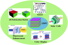
A one-dimensional photonic crystal (1DPC), which is a periodic nanostructure with a refractive index distribution along one direction, has been widely studied by scientists. In this review, materials and methods for 1DPC fabrication are summarized. Applications are listed, with a special emphasis on sensing platforms and photovoltaic devices together with full color display. After that, some typical 3D ordered structures with stacked layers are highlighted, fabrication methods are also described, and remaining problems are pointed out. Lastly, the possibility of building 3D stacked structures based on 1D layers through chemical routes is discussed; a relatively convenient and flexible method. We believe such a method is a promising way to conduct 3D fabrication.


image file: c5ra21373h-p1.tif

Huaizhong Shen

Huaizhong Shen received his B.S. degree in polymer science and engineering from the College of Material Science and Engineering, Jilin University, in 2011. He is now a PhD student in the State Key Lab of Supramolecular Structure and Materials of Jilin University, under the supervision of Prof. Bai Yang. His current research is the fabrication and characterization of ordered stacked structures and their optical applications.

image file: c5ra21373h-p2.tif

Zhanhua Wang

Zhanhua Wang received his PhD degree in Polymer Chemistry and Physics from Jilin University under the supervision of Prof. Bai Yang in 2011. After that, he worked as a postdoctoral fellow with Prof. Marek Urban in the University of Southern Mississippi and in Clemson University. Presently, he is a postdoctoral fellow in Prof. Han Zuilhof's group in Wageningen University and Research Center. His current scientific interests are focused on stimuli-responsive polymer composite photonic materials, bio-inspired self-healing and anti-fouling coatings.

image file: c5ra21373h-p3.tif

Yuxin Wu

Yuxin Wu was born in 1991. She obtained her B.S. degree in Applied Chemistry at the College of Chemistry, Jilin University, in 2014. She is currently a Masters student under the supervision of Prof. Bai Yang at Jilin University. Her research is centered on the nano/microscale fabrication of ordered array structures.

image file: c5ra21373h-p4.tif

Bai Yang

Bai Yang currently is a professor of the State Key Lab of Supramolecular Structure and Materials, in the College of Chemistry at Jilin University. He received his PhD in polymer chemistry and physics in 1991, under the supervision of Prof. Jiacong Shen at Jilin University. His research interests are concerned with polymeric micro- and nanostructures and functional materials, including optical, photonic, photo-electric and photo-responsive materials.


1. Introduction

Impressive examples existing in nature show delicate ordered structures,1 which endow so-called structural colors2–4 as well as multiple functions.5–7 The Morpho butterflies living in South America possess bright blue-colored wings, an example of a living creature with structural color,2 while the most famous plant is a multilayer-based example called Pollia, whose fruit exhibits an intense blue color derived from the interference of incident light inside the cell walls of the epicarp.8 Besides the modulation of light, nature's world also inspired people to imitate these intrinsic properties by mimicking the microstructures of various organisms. The orderly distributed arrays of nanometer-sized nipples on the compound eyes of some insects qualify as a good antireflective property.9 At the same time, voids occupied by air between the arrays provide controllable wettability of the surface.10–12 Various kinds of lamellar structures with good mechanical performance and multi-functionality, inspired by the natural structure of nacre, have also been fabricated.13–15 All of the properties we mentioned above motivate humans to reproduce these highly ordered structures according to application demands, thus making artificial construction of micro/nano structures an attractive research theme.

Although many efforts have been paid to mimic ordered three-dimensional structures,16–24 one-dimensional layered structures, well known as one-dimensional photonic crystals (1DPCs), also have been widely studied by scientists from basic theory to practical applications. Because of the periodic distribution of different refractive index materials along the stacking direction, multilayer interference within the films finally results in the elegant optical property of 1DPC called photonic band gap (PBG), which is defined as a waveband prohibiting light propagation. Bright and high-saturation color appears when PBG is located in the visible region, which makes 1DPCs a good candidate for applications such as a high-efficient reflector,25 chemical/physical sensor,26,27 dynamic color display,28 and so on. Recently, many methods have been developed to fabricate 1DPCs based on top-down as well as bottom-up construction routes,29,30 which we will discuss in detail in the next part.

However, with the rapid development of microfabrication technology, just replicating the natural world cannot meet emerging demands in materials applications. Thus, a hotspot since the beginning of the 21st century has been to construct new materials which do not exist in nature spontaneously;31 this can be classified as the study of meta-materials. Since the first man-made meta-surface was introduced,32,33 optical meta-materials have evolved towards realizing shorter working wavelengths together with multi stacks of the building blocks.34 Special focus is paid to the multi-stacking of building blocks so that, in the case of meta-materials, building blocks belonging to adjacent layers can strongly interact. Thus, it is very necessary for researchers of multilayer construction to study coupling states in 3D stacked meta-materials. An interesting aspect involved in understanding 3D multilayer stacks is that, to some extent, they can be considered as 1D ordered layer structures embedded with building blocks in specific layers such that the shape and size of the building blocks meet specific requirements. Then such stacks can be utilized to fabricate a 3D stacked meta-material. So, a question is raised: can this 3D fabrication route be realized based on 1D lamination? A detail discussion on this issue is given in part 8 of this review.

In this review, the present and ongoing progress in the field of 1DPC is first summarized. Common constituent materials and fabrication methods are introduced. When integrated with stimuli-responsive materials, 1DPCs are converted to smart materials which can respond to changes in the ambient environment. Applications of various kinds of 1DPCs are listed, with special emphasis on sensors and photo/electric devices. Next, the achievements and remaining problems with stacked 3D structures are listed. Our intention is to convey the idea that 3D meta-materials can be constructed through post-processing, especially routes involving chemical reactions, on the basis of 1D ordered layers.

2. Fabrication of high-quality 1D layered structure

2.1 Materials used in 1D layered structure fabrication

Various materials are utilized by scientists to make 1DPCs. Generally speaking, the constituent materials can be classified into three categories: inorganic materials, organic materials, and inorganic/organic hybrid materials. For 1DPCs made of inorganic materials, alternate stacks of SiO2 and TiO2 are mostly used.35,36 A typical cross-sectional morphology of 1D layer stacks comprised of SiO2 and TiO2 nano particles (NPs) is clearly shown in Fig. 1a by the Míguez group.37 A reflectance spectrum clearly shows the optical properties of samples with different constituent layers; a strong reflection (over 80%) is acquired within 8 bilayers because of the large difference between refractive index (RI) values of these two materials (the RI value of SiO2 thin film is 1.24 and the RI value of TiO2 thin film is 1.74, respectively). The wavelength region occupied by such strong reflection is defined as a PBG. The shape of the spherical NPs can be easily distinguished in the cross-sectional SEM image. When a defect layer which is about 3 to 5 times thicker than those layers forming the periodical stacks is intentionally inserted into the 1DPC, a photo cavity (i.e. a sharp dip in the reflection spectrum) will appear. Other efforts are also made to modify the property of a SiO2/TiO2 system by introducing new kinds of materials. One example is that GaAs is deposited inside the pores of a stack through a CVD method which yields a wider and more intense reflectance peak.38 Another is that, after conducting the monomer infiltration and the subsequent annealing procedure, PDMS is formed to convert the whole structure to be flexible and self-standing; this broadens its potential to be used as optical filter films or as an adhesive medium on lenses or mirrors.39 Besides the examples we have mentioned above, 1DPCs consisting of pure TiO2 or SiO2 have also been fabricated.40–42 Other kinds of inorganic NPs, including SnO2, ATO, ZnO, and Fe2O3, have also been used in 1DPC fabrication.43–45 Aside from NPs, Ozin and co-workers have successfully made use of chemically reactive clays to build 1DPCs, either entirely or in part. Basic optical properties and SEM images of cross-sectional morphology are shown in Fig. 1b. Clay is chosen for it is low-cost, low-toxicity, and ease of preparation. Its intrinsic ability of exchanging ions in an ambient environment makes it a promising material to transform a chemical signal to an optical response when coupled into a 1DPC structure.46–48
image file: c5ra21373h-f1.tif
Fig. 1 1DPCs consisting of different materials: (a) inorganic nanoparticles, reprinted from ref. 37 with permission of the American Chemical Society; (b) clays, reprinted from ref. 47 with permission of WILEY VCH; (c) and (d) pure polymer, reprinted from ref. 50 with permission of the American Chemical Society and ref. 54 with permission from Nature Publishing Group; and (e) polymer and inorganic titania sol, reprinted from ref. 56 with permission from WILEY VCH.

Similar to inorganic materials, polymers are also a good choice for preparing 1DPCs because of their responsiveness to diverse external stimuli through various kinds of functional groups.49 Furthermore, most of the fabrications using polymers involve a liquid operation; this process first makes a precursor using appropriate solvents, and then makes easy and low-cost thin films by spin coating or self-assembly. Until now, a large number of common polymers have been utilized in the fabrication of 1DPCs including polymethyl methacrylate (PMMA), polystyrene (PS), polyethylene (PE), polyethylene terephthalate (PET), etc.50–52 However, there are also disadvantages when using polymers. One is that polymers cannot withstand high temperatures, and thus 1DPCs made of polymers cannot operate under some extreme conditions; the other is that most of the common combinations of polymer thin-film layers possess tiny contrasts in RI value, which makes the PBG hard to achieve with small numbers of layers. A stack of over 200 repetition bilayers of 78 nm PMMA and 118 nm PET is clearly shown in Fig. 1c;50 it can be imagined that to finish this sample through traditional liquid processing would be very time-consuming, so a block copolymer was chosen to serve as a building material and thereby developed into a new fabrication method called block copolymer self-assembly.53 Block copolymer self-assembly is regularly undertaken by following two steps: first the copolymer precursor solution is spin coated onto a substrate, and then the copolymer film is exposed to solvent vapor annealing, which excites movement of polymer chains to form ordered layers simultaneously. Fig. 1d is a representative copolymer system of PS-b-P2VP developed by the Thomas group54 and there is no PBG when the block copolymer laminar stack is first established. However, the P2VP layers swell after being immersed in aqueous solvents, along with a change of RI value, which results in an obvious PBG. In order to increase the RI contrast, Kang and co-workers added one more step to modify the P2VP layer with SiO2 NPs.53

If only RI contrast is being considered, then a combination of polymer and inorganic materials should be the first choice, without hesitation. Usually, these two kinds of materials possess large contrasts in RI values and this leads to an obvious PBG with confined layers. An inorganic constituent often acts as an inert layer while a polymer is the functional layer to make a response to diverse stimuli. Gleason's group successfully built PHEMA/TiO2 stacks using chemical vapor deposition (CVD) to realize a fast response to water vapor.55 Fig. 1e shows the TEM image of TiO2 nano particles made by a sol–gel method and a highly ordered layer stack of alternate PHEMA/TiO2 fabricated through spin coating.56 Besides the traditional organic and inorganic building platform we described above, new materials never stop emerging, such as liquid crystals,57,58 zeolites,59,60 and semiconductors.61 Looking for more stable and multifunctional materials to build such structures will broaden the application fields of 1DPCs for practical use.

2.2 Fabrication methods used for 1D layered structure

With a variety of fabrication materials, developing suitable fabrication methods becomes significant. Up to now, the most widely used method has been spin coating. Spin coating can be applied to many materials, including NPs solutions,43 inorganic precursor sols,62 and polymer solutions.63 Generally speaking, spin coating begins with dropping a precursor solution on a flat substrate and then conducting the spin process to evaporate solvents. Usually, there will be an annealing procedure before spinning the next layer to solidify the as-prepared thin film; then the aforementioned steps will be repeated until the required number of layers is reached. Film thickness can be controlled by varying either cast solution concentration or rotation speed. An example of porous SiO2 and TiO2 1DPC through spin coating is given in Fig. 2a; the pores embedded in thin films can be infiltrated with different analytes, and this proves to be a good sensing platform.64 However, spin coating derives from a precursor solution; thus, successful fabrication requires carefully choosing solvents to avoid dissolution and penetration between the two constituent layers, which limits the selection of materials. Self-assembly is also a convenient method to fabricate 1DPCs including layer-by-layer (LBL), block copolymer and liquid crystals self-assembly. Since the early introduction of LBL deposition,65 LBL has become an important method for making 1DPCs. Unlike spin coating, the LBL method allows the deposition of thin films on curved surfaces, or even on spheres.66 Very thin films of several nanometers with opposite charges are alternately deposited by repeating sample immersion between the deposition and rinsing solutions. Fig. 2b shows a 1DPC consisting of a 4.5 period of 77-bilayer (PAH/PSS) and 24-bilayer(PAH/PAA) with silver NPs loaded in PAA layers.67 Even though the fabrication process can now proceed automatically with LBL coating robots, a hundred or more cycles of deposition is still a time-consuming process compared to spin coating. Based on the LBL method, Cohen and Rubner also developed an LBL-assisted self-assembly method to build SiO2/TiO2 1DPC.68 Traditional top-down etching methods are also used for preparing 1DPCs. 1DPC consisting of porous silicon can be fabricated by precisely controlling an electric pulse to generate different levels of porosity in separate layers (Fig. 2c),42 while wet-chemical etching can be used to destroy a sacrificial layer to form air/GaN layer stacks.61 Many other methods including chemical vapor deposition (CVD), physical vapor deposition (PVD), and molecular beam epitaxy have been also utilized to build 1DPCs.69–71
image file: c5ra21373h-f2.tif
Fig. 2 1DPCs derived using various approaches: (a) spin coating, reprinted from ref. 64 with permission of the American Chemical Society; (b) electrostatic layer-by-layer fabrication, reprinted from ref. 67 with permission of WILEY VCH, and (c) electric etching, reprinted from ref. 42 with permission of Elsevier B.V.

3. Basic theory of 1DPC and manipulation of PBG

In part 2 we mainly introduced constituent materials and fabrication methods for preparing a 1DPC, and we mentioned that, when integrated with some smart material, the as-prepared 1DPC can make a response to external stimuli. This raises a question: what kind of response is referred to? Actually, this is the most important aspect in studying 1DPC, which should be resolved as the means to modulate a photonic band gap. To explain this question, we first begin with the basic theory of 1DPCs. The position of a PBG (λBragg) and the stop band width (W) can be calculated by the following equations:2,72,73
image file: c5ra21373h-t1.tif

image file: c5ra21373h-t2.tif
where m is diffraction order, D is the thickness of the unit cell (D = dh + dl, dh + dl is the thickness of the two constituent layers, respectively), θ is the incident angle, nh + nl is the refractive index of the two layers, and neff is the effective refractive index. Effective refractive index can be estimated as:
neff = (nhdh + nldl)/(dh + dl)

Thus, in most cases of the vertical incidence, θ = 0°, the position of PBG can be calculated as following the simplified equation:

Bragg = 2(nhdh + nldl)
from which we may draw a conclusion that the position of a PBG is mainly determined by the optical thickness (defined as refractive index multiplied by layer thickness) of the layers. So, the modulation of a PBG can be realized simply by either changing the refractive index or the film thickness of the constituent layers. Generally speaking, the position of a PBG will red-shift with an increase of film thickness. In fact, in practical uses for sensing based on a PBG change, most cases are designed according to the above theory, which a previous review summarized as “sensing by pore filling” and “sensing by swelling.”72 In the next part, detailed examples of 1DPCs being used as sensing platforms are shown.

4. 1DPCs used as sensing platforms: selected examples

4.1 1DPC sensors for physical stimuli

Abundant changes of surrounding conditions may trigger the shift of a PBG and these can be mainly divided into physical, chemical, and biological stimuli.74 In the case of physical stimuli, the shift of a PBG is realized mainly by volume change of a specific layer or an analyte-induced refractive index change. Gong's group has developed a kind of rubber-like elastic hydrogel in which a double network principle is applied to form a second PAAm network inside the as-prepared PAAm layer.75 This hydrogel exhibits fast and reversible color change when external stretch or compression is applied or released. The PBG can be tuned through the whole visible range spectrum (Fig. 3a), thus making it a good platform for visual detection of a mechanical field. Stafford, Chan and co-workers also built a mechanochromic sensor based on a PS-b-P2VP structure.76 The relationship between the mechanical response and PBG change was established to quantify the soft material mechanics and this block copolymer based sensor can be made into conformal coatings which can be used on various shaped surfaces. Huang's group built a nanoporous 1DPC through holographic interference patterning for humidity sensing.77 When water vapor fills the pores in the porous layer, the RI value of those layers changes, thus inducing a modification of the RI value contrast which is finally reflected in the transmittance spectra (Fig. 3b). With the same function of humidity sensing, Yang's group fabricated a hybrid 1DPC structure consisting of PHEMA and TiO2 through spin coating.56 In this case, the PBG shift was caused by the polymer layer swelling. Reflection spectra of the sample exposed to different concentrations of water vapor were tested and the results showed that with a more condensed water vapor atmosphere the PBG shifted to longer wavelengths, thus indicating that the polymer layer swelled to a larger extent. A previous study showed that N-isopropylacrylamide (NIPAm) is thermosensitive78,79 and Yang's group fabricated a 1DPC which responded to temperature change by integrating the PNIPAm layer.80 When the temperature increased, the hydrophilic film became hydrophobic as 32 °C was exceeded; thus the film lost water molecules which were absorbed at a lower temperature. The refractive index of the PNIPAm layer then increased and the RI value contrast dramatically narrowed; this led to the PBG intensity decreasing, and thus the sample color vanished (Fig. 3c). Brinke and Ikkala realized a large and reversible switching of a PBG in the solid phase based on a polymer self-assembly structure consisting of polystyrene-block-poly(4-vinylpyridinium methanesulphonate) (PS-b-P4VP(MSA)) and 3-n-pentadecylphenol (PDP) to form a lamination.81 At room temperature, PDP is a selective solvent just for the P4VP(MSA) layer, due to hydrogen bonding, but after heating above 125 °C, the hydrogen bonding between PDP and P4VP(MSA) is broken and PDP starts to migrate into the PS domain, which then leads to collapse in the P4VP(MSA) microstructure. Thus, the period decreases and the PBG shows a blue-shift. Electrically controlled color-tunable 1DPC also has been studied by many researchers and we will introduce them in part 5.
image file: c5ra21373h-f3.tif
Fig. 3 1DPCs with ability to respond to physical signals: (a) reversible color tuning of a 1DPC through tensile elongation, reprinted from ref. 75 with permission of the American Chemical Society; (b) PBG shift with change of humidity, reprinted from ref. 77 with permission of Elsevier B.V.; (c) reflectance spectra and photographs under different temperatures, reprinted from ref. 80 with permission of the Royal Society of Chemistry.

4.2 1DPC sensors for chemical/biological stimuli

Also, large numbers of 1DPCs with chemical responsiveness have been built by scientists. Yang's group fabricated a series of hybrid 1DPCs consisting of different kinds of stimuli-responsive polymer and titanium dioxide. When poly(N,N-dimethylaminoethyl methacrylate) (PDMAEMA) is selected,82 the amino group in the polymer layer can accept protons and then swell in acidic solutions, as a result of an electrostatic repulsion which endows the structure with pH responsiveness (Fig. 4a). Furthermore, if this 1D Bragg stack is immersed in a mixture of glucose and glucose oxidase, the reaction of these two reactants can induce a change of solution pH and thus the pH-sensitive 1DPC can act as a real-time detector for the reaction process. The PDMAEMA-based 1DPC can also be used for SCN detection;83 when a quaternized sample is immersed in a SCN solution, the PBG will blue-shift, which is caused by volume collapse resulting from the weakened electrostatic repulsion inside polymer layers. Various concentrations of SCN solutions can be distinguished by different colors, in spite of the presence of other anions (Fig. 4b). When the polymer layer is formed by poly methyl methacrylate-co-hydroxyethyl methacrylate-co-ethylene glycol dimethacrylate (PMMA-co-PHEMA-co-PEGDMA), 1DPC possesses the ability to differentiate a series of organic solvents from one another by exhibiting different extents of PBG red-shift when reaching the film swell balance (Fig. 4c).84 Recently, 1DPCs based on polymer and graphene oxide were also built for solvent and pH detection.85,86 As mentioned above, clays were utilized by the Ozin group to fabricate 1DPCs because of their easy and low-cost fabrication process and intrinsic chemical reactivity of taking up and releasing specific ions or surfactants. The PBG shift of the sample exposed to surfactants solution in ethanol is shown in Fig. 4d;47 this surfactant sensor can be used for many cycles because the sodium state in a LAPONITE® layer may regenerate through exposure to a NaCl solution (Fig. 4e).46 Another very important sensing platform is porous 1DPC. Until now, organic solvent vapor-, pH-, and oxygen-sensitive 1DPCs have been synthesized depending on the mechanism of pore filling.72 Especially, mesoporous TiO2 and SiO2 1DPCs, fabricated through spin coating, have enhanced sensitivity to analytes when compared with 1DPCs consisting only of a single porous layer.64 Efforts to improve sensing selectivity were also made by precisely controlling the pore size. A porous silicon double layer stack was assembled by Sailor's group to be used as a bovine serum albumin (BSA) detector.87 When the BSA detector was exposed to a mixture of BSA and other small molecules, only BSA was captured while the small molecules penetrated the structure. Instead of the above-mentioned porous structure, Mígueze inserted a single porous layer between two periodic multilayers to generate an intense optical cavity in reflectance spectra.88 Size-selective detection was also evaluated, by studying the relationship between the pore size and probe-molecule size. A block copolymer self-assembly system comprised of PS-b-P2VP was also sensitive to pH and other ions because the quaternized P2VP layer may adopt or lose protons in the solution.54,89 Other solvent-responsive 1DPC sensors were also developed based on various materials including gold NPs, Teflon polymer, metallic osmium, and so on.90,91 In the cases of 1DPCs being used as bio-sensors, the response mechanism is more or less the same,92 while the probe-analytes are mainly biological molecules containing fructose,93 protein,27 bacteria, etc.94
image file: c5ra21373h-f4.tif
Fig. 4 1DPCs with response to chemical stimuli: (a) reflectance spectrum of a pH-sensitive 1DPC under different pH values, reprinted from ref. 82 with permission of the Royal Society of Chemistry; (b) specific detection of SCN in the presence of other anions, reprinted from ref. 83 with permission of the Royal Society of Chemistry; (c) PBG shift and corresponding photographs of 1DPCs when immersed in different organic solvents, reprinted from ref. 84 with permission of the Royal Society of Chemistry; (d) surfactants detection through porous 1DPC, reprinted from ref. 47 with permission of WILEY VCH; and (e) the stability of 1DPC after cyclic tests, reprinted from ref. 46 with permission of the American Chemical Society.

4.3 Aspects remaining to be improved in 1DPC sensors: a brief outlook

Many examples have been given to show achievements to date in using 1DPCs as sensors and from these we can see that a wide range of target objects can be detected by incorporating an appropriate responsive layer into a photonic structure. Compared with other sensing structures, for example the SPR structure, a photonic crystal is easy to prepare with large area and it can be flexible under certain manufacturing processes. A noble metal-free structure also helps lower the fabrication costs. Besides, visible read-out brought within the visible range by a PBG shift is a convenient and practical use. There is no doubt that further study will produce more 1DPCs with multiple functions. Generally speaking, progress should be in accordance with the following basic guidelines: the fabrication process should be environmentally friendly and non-toxic or low-toxicity materials should mainly be used. Easy and economical methods should be applied to the 1DPC fabrication. In most instances, the as-prepared sensors need to be recycled for repeated use. Furthermore, scientists are seeking to improve sensing performance. High sensitivity comes first and we can imagine that, in the case of mechanochromic 1DPC,76 if the sensitivity is further enhanced then this platform may be used to trace movements of cells and bacteria on specific surfaces. Quick response is also significant for realizing real-time detection. Furthermore, detection favoring one analyte rather than “one kind” is in great demand; thus, more specific chemical reactions should be combined with a 1DPC structure to induce a PBG shift. Last but not least, a facile optical read-out is favoured, which means that a PBG is best located within the visible range of the spectrum; thus, the stimuli-response can be finally transferred into a visible signal for the naked eye. However, with the development of interdisciplinary initiatives, new technologies should be integrated with 1DPC sensors. Ozin and his group set a good example when they developed the concept of the “photonic nose” which combines together surface-modified NP porous 1DPC arrays and digital-color image principal-component analysis.94,95 The as-prepared 1DPC arrays are designed to analyze both liquid and vapor phases. With the help of a component analysis method, this device successfully identifies different kinds of molecular species and several types of pathogenic bacteria.

5. 1DPC used in photo/electric devices

1DPCs are not only widely used in the field of sensors, but also are integrated into photo/electric devices. Many efforts have been made to utilize 1DPCs as back reflectors to enhance the efficiency of photovoltaic devices.72 Míguez and co-workers used a porous SiO2/TiO2 Bragg stack together with a dye-sensitized solar cell to achieve an amplified light absorption to enhance the power conversion efficiency.96 They further developed a flexible system based on porous SiO2/TiO2 1DPC which has the potential to be coupled with polymer solar cells.39 In Fig. 5a we show a device structure coupled with an 8-pair 1DPC and polymer solar cell which has been designed by Ruan and co-workers.97 By optimizing the band position of a WO3/LiF 1DPC, it enhances light harvesting in the absorbing layer, thus making a great contribution to increasing the power conversion efficiency (PCE) by 21.7%. However, finding a way of combining together the optimal design of 1DPC and the solar cells is not always easy. Thus, Tétreaultand co-workers developed a kind of 1DPC consisting of SiO2 and tin-doped indium oxide (ITO) which was conductive.98 This 1DPC system can be used as electrode material to replace a traditional counter electrode and the short circuit current density was increased by up to 40% with different light intensities (Fig. 5b). Other attempts to develop conductive 1DPCs can also be found elsewhere.99 Except for experimental verification, complete theoretical analysis for the coupling of 1DPCs and solar cells is also thriving;100–102 tuning PBGs and broadening reflectance bandwidth has been discussed by scientists to guide better design of such reflectors.
image file: c5ra21373h-f5.tif
Fig. 5 (a) 1DPC used as back reflector to improve the PCE of a semi-transparent polymer solar cell, reprinted from ref. 97 with permission of the American Chemical Society; (b) increase of current density through using a conductive 1DPC as electrodes, reprinted from ref. 98 with permission of the WILEY VCH; and (c) electrical induced tuning of structural color of a 1DPC, reprinted from ref. 107 with permission of the Royal Society of Chemistry.

Electric field-sensitive 1DPCs is another important category of responsive structure. An optical switch was realized using a dye-doped polymeric photonic crystal103 and the transmittance state could be shifted between on and off through applying a voltage. With a similar function, a lower tuning voltage was realized through a liquid crystal based layer-like structure.104 A very promising application for electric-sensitive 1DPCs is full color display because of its intrinsic high brightness and saturation structural color, which is tunable under applied voltage stimulus. Scientists have made some progress in this field. The PS/P2VP system is ionic strength-sensitive and the P2VP layer is charged when immersed in an electrolyte. An applied electric field will change the chemical environment (i.e. the ion strength) around the 1DPC; thus the P2VP layer will swell or shrink leading to the PBG shift.105,106 Actually, the change in layer thickness is induced by the chemical change of the ambient environment directly, while this chemical change is controlled by an external electric field, which makes the electrical tuning occur. As shown in Fig. 5c, the sample immersed in a liquid reservoir displays blue color with no external electric field. However, the P2VP layer swells after the system is electrified and the PBG shifts to a longer wavelength, which results in the color change to green and further to orange.107 Besides the tuning of a PBG position, tuning of bandwidth is realized with a NiO/WO3 based 1DPC.108 The broadening of band width is caused by the RI change of both constituent layers, which derives from an electrical-induced redox reaction. This may help improve grayscale control in reflective displays. Even though many efforts have been made to achieve full color display, some problems remain to be solved before practical applications. The first is to realize a low drive voltage to make the display device work, which is a benchmark of high-sensitivity and also saves energy. Another criterion for color display is the response time, which is quite important for good reproduction of dynamic scenes. However, shortening the response time relies on the material involved in 1DPC fabrication and the reaction theory combined with the as-prepared structure. And the most challenging objective is to realize all of the above in a solid phase without any liquid, which is crucial for mass production and subsequent use in daily life. Much still remains for scientists to further explore.

6. Other applications

As a structure of spatially periodic refractive index distribution, 1DPCs have the ability to tune electromagnetic waves (EM waves) and they have been utilized to fabricate omnidirectional reflectors whose PBGs are insensitive to the incident angle and polarization of EM waves.109,110 Fine tuning of the bandwidth and frequency range of such structures was achieved. Besides, modulation of fluorescence emission using 1DPCs is also attractive for scientists and much research can be found in this field. Photonic crystal-based laser emission is one of the research interests in this area. Komikado et al. fabricated a Rhodamine 6G (R6G)-doped polymeric 1DPC,111 as shown in Fig. 6a. When this structure was excited by a pump laser, the dye laser emitted vertically from the surface of the 1DPC. The narrow emission peak was attained at the designed position (the blue band edge of the photonic stop band) while the emission above 590 nm was totally suppressed. Besides the laser emitter based on dyes, other laser emitters based on NPs have also been reported.112,113 Recently, dual-emitting quantum dots (QDs) were considered promising for use in a QD sensor; Chen and co-workers used a photonic crystal structure to enhance normal direction excitation and emission of dual-emitting QDs, which improved sensitivity and resolution.114 1DPCs are also good platforms to obtain enhanced fluorescence because the intensity will become highest when the pump photon energy coincides with the photonic band edge.115,116 Fig. 6b shows an obvious difference between the traditional bulk-like structure and the 1D layered structure doped with quantum dots as fluorescence agents.117 Reflectance spectra clearly show the different intensities of these two samples; the layer-based structure's reflection is much higher than the ordinary bulk one. Apart from luminescent related applications, a multilayer stack with tandem and gradient structure distribution was fabricated with a broad reflectance which may span the entire visible range.118 This special structure may have potential to be applied in fields such as photo catalysis and optical sensing.
image file: c5ra21373h-f6.tif
Fig. 6 (a) 1DPC-based organic dye laser device, reprinted from ref. 111 with permission of the AIP Publishing LLC.; (b) enhanced fluorescence from CdSe/ZnS quantum dots embedded in a 1DPC backbone structure, reprinted from ref. 117 with permission of the Royal Society of Chemistry.

7. Highly ordered 3D structure with stacking characteristic

Not only are 1DPCs widely studied by scientists; many studies have also been reported in the field of fabricating 3D ordered structures including opals, inverse opals, chiral structures, biomimetic structures, etc.17,119–123 A colloidal crystal is a representative structure and scientists have successfully utilized silica colloids as well as PS colloids to fabricate 3D structures.124–126 Depositing multilayers on non-planar surfaces is an alternative way to carry out 3D construction and some bio-inspired structures with specific functions have been fabricated in this way.127–130 Previous reviews summarized various methods in 3D micro/nano fabrication.20,131–134 However, in this review we mainly focus on highly-ordered 3D structures with multilayer stacks. Many outstanding studies have been reported in this field. Such 3D structures at the micrometer scale have been fabricated for use as bioactive scaffolds to study cell development in a controlled environment.135–137 With the emergence of new fabrication technology, building stacked 3D structures at the nano scale has now been realized.138 The most representative research is stacked meta-material.139–144 Meta-materials can be considered as a class of materials made artificially with properties which do not exist in nature, including negative refractive index, negative magnetic permeability, perfect absorbance, etc. The possible application fields of such materials are ultrahigh-resolution super lenses, communication antennas, magnetic recording media, cloaking materials, and so on. Compared to a 1DPC, which is of equal size to the wavelength of light, meta-materials consist of packed building blocks which are smaller than the wavelength of light. Following its first experimental realization,33 the study of meta-materials is prospering.145–147 In place of the early research, which was mainly focused on the meta-surface, recent studies are committed to realizing the fabrication of meta-materials with multi-functional layers so that the building blocks belonging to adjacent layers can strongly interact and meet practical applications which require real 3D bulk-like structures.31,34 Selected examples of 3D structures with stacked layers are shown in Fig. 7.148–150 A 12-layer woodpile structure was fabricated by direct laser writing and subsequently selectively metalized with a silver coating (Fig. 7a). The as-prepared structure is conductive and the second band gap is located in the visible range. This is the first metalized structure with a 100 nm resolution. Fig. 7b shows a multilayer fishnet structure consisting of 30 nm silver and 50 nm magnesium fluoride. This is the first 3D optical experimentally made negative-index meta-material where the negative refractive index is derived from the negative magnetic and electric properties. The modulation of light can be measured directly by using a prism built into the multilayer stack. When light passes through the prism, a change in propagation direction occurs. Thus, observing the refraction angle provides a simple and visualized way to determine the refractive index of the system.
image file: c5ra21373h-f7.tif
Fig. 7 Selected examples of stacked 3D ordered structures: (a) woodpile structure with 12 layers, reprinted from ref. 148 with permission of WILEY VCH; (b) 21-layer fishnet structure, reprinted from ref. 149 with permission of Nature Publishing Group; and (c) a 4-layer stack of a split-ring resonator, reprinted from ref. 150 with permission of the Nature Publishing Group.

Another very representative unit cell in fabricating meta-material is a split-ring resonator (SRR), which is shown in Fig. 7c. The four-layer SRR structure was constructed through a layer-by-layer technique which involved planarization, lateral alignment, and stacking. A new characteristic spectral feature brought by the vertical interaction between the constituent layers was studied; an increase in bandwidth was found with the increasing number of stacked layers. This can serve as a basic foundation for the further design of broadband meta-material.

The emergence of the above-mentioned delicate 3D structures actually relies on newly developed fabrication methods. Until now, various techniques, including the template method, angular exposure deposition, and interference lithography, were utilized to form layer-like 3D structures.151–153 However, the most widely used method in multilayer 3D fabrication is a layer-by-layer technique in which two main steps are involved: one is the fabrication of layers containing building blocks, and the other is stacking of the as-prepared single layers.140,141,150,154,155 Optical lithography is a well-established technique to form building blocks inside a single film. The resolution of the patterns is repeatedly refreshed by employing smaller wavelength light sources, from ultraviolet to extreme ultraviolet (EUV).156,157 While seeking smaller patterns beyond the diffraction limit of light, state-of-the-art techniques such as electron-beam lithography, interference lithography, and direct laser writing have been applied to make various building blocks in an individual layer.29,144,158 After obtaining a single film, the next step is to assemble multiple layers. However, unlike the planar layers assembly, the non-planar layer containing patterns on the surface may hinder the stacking. To overcome this problem Giessen et al. added a planarization procedure before the stacking process to planarize the single film.150 But, another crucial step for layer stacking, called lateral aligning, is still needed, together with an additive process of making alignment markers. It is very difficult to achieve high resolution alignment in multilayer fabrication and that explains the reason why the number of stacking layers is theoretically unlimited but actually is confined in practice.

8. 1D layered structure: a universal matrix for 3D construction?

From the discussion above, we may draw a conclusion that only a limited number of layers can be obtained by forming building blocks ahead of layer stacking. So, an alternative route is proposed: that is, building a 1D layered structure first and then conducting a post-processing step to form building blocks inside the multilayers. The advantage is that the desired number of layers can be obtained at one time; all the material and fabrication methods we summarize for 1DPCs fabrication can be utilized to build the reactive layers together with inert spacer layers. The layer thickness can be tuned as needed, which makes the study of building-blocks coupling as a function of interlayer spacing easy. However, the key to realizing this goal lies in the post-processing step. Metal-ion doped polymer film can be a good choice because the chemical reaction between some metal ions and external irradiation may occur under mild conditions. Yang's group chose 1DPC doped with silver ions to fabricate building blocks inside a multilayer,159 as is shown in Fig. 8. A polymer 1DPC consisting of PMMA and PVA with silver ions in PVA layers was first fabricated by spin coating. Then, by using an appropriate photo mask, silver ions exposed to UV light were reduced to form 3D silver networks inside the 1DPC. This is a very representative fabrication route to build 3D layer stacks by a post-processing step. The size and shape of the building blocks can be tuned through changing masks; the PMMA layer thickness is flexibly tunable and thus the desired distance between adjacent building blocks can be obtained easily. This process also omits the aligning step which confines the total number of layers. However, this is just a preliminary trial to build 3D structures through a post-process and there remains much to be improved in the future. The most important aspect is to form building blocks in a much smaller size scale. We anticipate that with light of shorter wavelength utilized in the irradiation step, the resolution of building blocks can be further improved. Compared to the above work, a more imaginative idea emanates. Consider that if we build a 1D matrix layer doped with two different reagents belonging to two kinds of constituent layers respectively, and if the chemical change of the reagents can be induced in different situations, then a twisted 3D layered structure160 could form after two independent exposure processes. However, the choice of material and careful selection of chemical reactions still remain a big challenge to realizing this idea in practice. The in situ formation of silver NPs inside a single polymer film has also been reported by other researchers.161,162 Besides silver, a gridding microstructure consisting of gold was fabricated through direct laser writing, which is a maskless approach,163 as shown in Fig. 9a. Chemical properties of a polymer may also serve as a means to build a 3D structure. As shown in Fig. 9b, with a 1DPC containing a photo initiator and a photo mask on top of it, selective parts are crosslinked by UV light, thus producing chemical patterns in selective layers which can be considered as a 3D structure with layer stacks.80 Sivaniah et al. have also developed an ordered 3D material made of commercially available polystyrene-block-polymethyl methacrylate (PS-b-PMMA). They first spin cast this copolymer solution on a silicon substrate, and then exposed it to UV light to perform PS cross-linking and PMMA degradation before immersing it in acetic acid. Once immersed in the acid, PMMA oligomers begin to dissolve and leave behind the PS stacked layers supported by PS columns.164 One problem remaining with this method is that the ordering needs to be further improved. Furthermore, another route to make 3D structures based on the 1D layers, proposed by Boltasseva, involved anisotropic etching on deposited metal-dielectric layers (Fig. 9c).165 Properly choosing the etch-resistant mask is crucial for ensuring successful acquirement of a fishnet structure using this method.
image file: c5ra21373h-f8.tif
Fig. 8 Schematic illustration of building a 3D silver network through post-processing: a 1D layered structure containing Ag+ is first fabricated by spin coating and then it is exposed to UV light under a specific photo mask to perform an in situ reduction process, reprinted from ref. 159 with permission of the Royal Society of Chemistry.

image file: c5ra21373h-f9.tif
Fig. 9 Some possible routes involving chemical reactions that can be utilized to perform 3D construction: (a) direct laser writing to form a gold microstructure, reprinted from ref. 163 with permission of the AIP Publishing LLC.; (b) UV crosslinking of specific polymer layers in situ in a 1D lamination, reprinted from ref. 80 with permission of Royal Society of Chemistry; and (c) a possible method to build a 3D structure by anisotropic etching presented in ref. 165, reprinted with permission of the Elsevier B.V.

9. Conclusions and perspectives

In this review, we have summarized the materials and methods to generate one dimensional photonic crystals. Based on the constituent material, 1DPCs can be divided into three major categories: inorganic 1DPCs, organic 1DPCs, and inorganic/organic hybrid 1DPCs. Due to periodical refractive index distribution along the stack direction, a photonic band gap will appear in a corresponding position of the spectra and it is mainly depended on the effective RI and period thickness. Thus, changing the RI value of a specific layer will lead to the shift of a PBG which is mostly used in the case of porous inorganic 1DPCs by filling the pores. A PBG shift induced by layer swelling or shrinkage is the result that often happens in a 1DPC composed of polymer layers. The PBG shift can be utilized within the visible range to perform visual detection. However, the newly emerging risks for social security and public health are both a challenge and an opportunity for 1DPC sensors. Sensors of high specificity to target analytes, such as explosive and virus molecules, are in high demand and integrated sensor devices are favored. 1DPCs used in photo/electric devices have also been discussed, with emphasis an on photovoltaic and electrochromic devices and the feasibility of a full color display through an electrochromic 1DPC. Future studies in the 1DPCs field should focus on these aspects: (1) innovation of ultrafast, low-cost methods for the fabrication process, (2) realization of a faster and larger tuning range of PBGs, and (3) combination with new technology to expand the 1DPC-based sensing scheme. Recently, a new integrated 1DPC sensor was reported;166 various light sources and photodetectors were utilized to realize real-time monitoring of analyte diffusion and cell adherence behavior with facile electro-signal read-out. This new concept of a “three in one” device represents a new trend in 1DPC-based sensors.

Next, we have briefly introduced the 3D ordered structure with characteristics of stacked layers. Three representative structures are exemplified: woodpile, fishnet, and SRR stacks. These 3D structures are of great interest for their potential applications with a bio-compatible matrix and meta-materials. The layer-by-layer fabrication method for 3D stacked structures has been highlighted as being the most widely used. The advantage of such a method is that all the methods which can fabricate patterns in single layers can be utilized, while the disadvantage is that a mismatch in the stacking process will limit the actual number of layers that can be attained. So, more convenient and effective approaches to construct such 3D stacked structures need to be developed. Considering that both 1DPCs and stacked 3D structures involve multilayer stacks, we propose an alternative method which is a combination of a bottom-up fabrication of the layered structure and subsequently, a top-down post-processing step converting it into a 3D structure. Many methods can be utilized to fabricate 1D laminations at different size scales, such as spin coating, dip coating, and self-assembly. Some possible routes, especially those involving chemical reactions, are suggested, including in situ formation of building blocks inside a metal ion doped thin film, reactive anisotropic etching, and photo-crosslinking of polymer films. The possibility of building 3D layered structures based on 1D layers has also been discussed. However, some of the concepts still remain to be verified by experimentation. It is remarkable that in the first decade of the 21st century, scientists have made milestone achievements in the study of 3D meta-materials to bring the working frequency from the microwave to the visible range. Other studies, such as loss compensation in a metallic 3D meta-material, building of an all-dielectric 3D structure, and large-scale fabrication techniques, are still ongoing. We believe that in the near future our proposal will be experimentally verified, thereby helping to solve the above problems and contributing to the large-scale fabrication of 3D stacked meta-materials for daily use.

Acknowledgements

This work was financially supported by the National Science Foundation of China (NSFC) under Grant No. 91123031, 21221063, 51373065 and the National Basic Research Program of China (973 Program) under Grant No. 2012CB933800.

References

  1. J. Xu and Z. Guo, J. Colloid Interface Sci., 2013, 406, 1–17 CrossRef CAS PubMed .
  2. S. Kinoshita and S. Yoshioka, ChemPhysChem, 2005, 6, 1442–1459 CrossRef CAS PubMed .
  3. I. B. Burgess, M. Lončar and J. Aizenberg, J. Mater. Chem. C, 2013, 1, 6075–6086 RSC .
  4. Y. Zhao, Z. Xie, H. Gu, C. Zhu and Z. Gu, Chem. Soc. Rev., 2012, 41, 3297–3317 RSC .
  5. Y. Li, J. Zhang and B. Yang, Nano Today, 2010, 5, 117–127 CrossRef .
  6. K. Liu and L. Jiang, Nano Today, 2011, 6, 155–175 CrossRef CAS .
  7. K. Liu, Y. Tian and L. Jiang, Prog. Mater. Sci., 2013, 58, 503–564 CrossRef CAS .
  8. S. Vignolini, P. J. Rudall, A. V. Rowland, A. Reed, E. Moyroud, R. B. Faden, J. J. Baumberg, B. J. Glover and U. Steiner, Proc. Natl. Acad. Sci. U. S. A., 2012, 109, 15712–15715 CrossRef CAS PubMed .
  9. D. G. Stavenga, S. Foletti, G. Palasantzas and K. Arikawa, Proc. R. Soc. B, 2006, 273, 661–667 CrossRef CAS PubMed .
  10. G. S. Watson and J. A. Watson, Appl. Surf. Sci., 2004, 235, 139–144 CrossRef CAS .
  11. T. L. Sun, L. Feng, X. F. Gao and L. Jiang, Acc. Chem. Res., 2005, 38, 644–652 CrossRef CAS PubMed .
  12. J. X. Wang, Y. Z. Zhang, S. T. Wang, Y. L. Song and L. Jiang, Acc. Chem. Res., 2011, 44, 405–415 CrossRef CAS PubMed .
  13. H. B. Yao, H. Y. Fang, Z. H. Tan, L. H. Wu and S. H. Yu, Angew. Chem., Int. Ed., 2010, 49, 2140–2145 CrossRef CAS PubMed .
  14. C. Li, J. Adamcik and R. Mezzenga, Nat. Nanotechnol., 2012, 7, 421–427 CrossRef CAS PubMed .
  15. H. B. Yao, J. Ge, L. B. Mao, Y. X. Yan and S. H. Yu, Adv. Mater., 2014, 26, 163–188 CrossRef CAS PubMed .
  16. A. Stein, B. E. Wilson and S. G. Rudisill, Chem. Soc. Rev., 2013, 42, 2763–2803 RSC .
  17. T. G. Leong, A. M. Zarafshar and D. H. Gracias, Small, 2010, 6, 792–806 CrossRef CAS PubMed .
  18. N. Tetreault, H. Míguez and G. A. Ozin, Adv. Mater., 2004, 16, 1471–1476 CrossRef CAS .
  19. X. Ye and L. Qi, Nano Today, 2011, 6, 608–631 CrossRef CAS .
  20. C. Paquet and E. Kumacheva, Mater. Today, 2008, 11, 48–56 CrossRef CAS .
  21. D. J. Shir, S. Jeon, H. Liao, M. Highland, D. G. Cahill, M. F. Su, I. F. El-Kady, C. G. Christodoulou, G. R. Bogart, A. V. Hamza and J. A. Rogers, J. Phys. Chem. B, 2007, 111, 12945–12958 CrossRef CAS PubMed .
  22. J. H. Lee, C. Y. Koh, J. P. Singer, S. J. Jeon, M. Maldovan, O. Stein and E. L. Thomas, Adv. Mater., 2014, 26, 532–569 CrossRef CAS PubMed .
  23. Y. Zhao, L. Shang, Y. Cheng and Z. Gu, Acc. Chem. Res., 2014, 47, 3632–3642 CrossRef CAS PubMed .
  24. J. H. Moon and S. Yang, Chem. Rev., 2010, 110, 547–574 CrossRef CAS PubMed .
  25. A. Bruyant, G. Lerondel, P. J. Reece and M. Gal, Appl. Phys. Lett., 2003, 82, 3227–3229 CrossRef CAS .
  26. O. Sanchez-Sobrado, G. Lozano, M. E. Calvo, A. Sanchez-Iglesias, L. M. Liz-Marzan and H. Míguez, Adv. Mater., 2011, 23, 2108–2112 CrossRef CAS PubMed .
  27. F. Frascella, S. Ricciardi, P. Rivolo, V. Moi, F. Giorgis, E. Descrovi, F. Michelotti, P. Munzert, N. Danz, L. Napione, M. Alvaro and F. Bussolino, Sensors, 2013, 13, 2011–2022 CrossRef CAS PubMed .
  28. S. H. Lee and N. Y. Ha, Small, 2011, 7, 2704–2708 CrossRef CAS PubMed .
  29. A. Biswas, I. S. Bayer, A. S. Biris, T. Wang, E. Dervishi and F. Faupel, Adv. Colloid Interface Sci., 2012, 170, 2–27 CrossRef CAS PubMed .
  30. G. von Freymann, V. Kitaev, B. V. Lotsch and G. A. Ozin, Chem. Soc. Rev., 2013, 42, 2528–2554 RSC .
  31. Y. Liu and X. Zhang, Chem. Soc. Rev., 2011, 40, 2494–2507 RSC .
  32. R. A. Shelby, D. R. Smith and S. Schultz, Science, 2001, 292, 77–79 CrossRef CAS PubMed .
  33. D. R. Smith, W. J. Padilla, D. C. Vier, S. C. Nemat-Nasser and S. Schultz, Phys. Rev. Lett., 2000, 84, 4184–4187 CrossRef CAS PubMed .
  34. C. M. Soukoulis and M. Wegener, Nat. Photonics, 2011, 5, 523–530 CAS .
  35. M. C. Fuertes, S. Colodrero, G. Lozano, A. R. Gonzalez-Elipe, D. Grosso, C. Boissiere, C. Sanchez, G. Soler-Illia and H. Míguez, J. Phys. Chem. C, 2008, 112, 3157–3163 CAS .
  36. P. Kurt, D. Banerjee, R. E. Cohen and M. F. Rubner, J. Mater. Chem., 2009, 19, 8920–8927 RSC .
  37. S. Colodrero, M. Ocana and H. Míguez, Langmuir, 2008, 24, 4430–4434 CrossRef CAS PubMed .
  38. O. Sánchez-Sobrado, K. Thomas, I. Povey, M. E. Pemble and H. Míguez, Small, 2010, 6, 1283–1287 CrossRef PubMed .
  39. M. E. Calvo and H. Míguez, Chem. Mater., 2010, 22, 3909–3915 CrossRef CAS .
  40. M. E. Calvo, S. Colodrero, T. C. Rojas, J. A. Anta, M. Ocaña and H. Míguez, Adv. Funct. Mater., 2008, 18, 2708–2715 CrossRef CAS .
  41. L. Dal Negro, M. Stolfi, Y. Yi, J. Michel, X. Duan, L. C. Kimerling, J. LeBlanc and J. Haavisto, Appl. Phys. Lett., 2004, 84, 5186–5188 CrossRef CAS .
  42. M. Qian, X. Q. Bao, L. W. Wang, X. Lu, J. Shao and X. S. Chen, J. Cryst. Growth, 2006, 292, 347–350 CrossRef CAS .
  43. D. P. Puzzo, L. D. Bonifacio, J. Oreopoulos, C. M. Yip, I. Manners and G. A. Ozin, J. Mater. Chem., 2009, 19, 3500–3506 RSC .
  44. E. Redel, P. Mirtchev, C. Huai, S. Petrov and G. A. Ozin, ACS Nano, 2011, 5, 2861–2869 CrossRef CAS PubMed .
  45. J. R. Chen, T. C. Lu, Y. C. Wu, S. C. Lin, W. R. Liu, W. F. Hsieh, C. C. Kuo and C. C. Lee, Appl. Phys. Lett., 2009, 94, 061103 CrossRef .
  46. B. V. Lotsch and G. A. Ozin, ACS Nano, 2008, 2, 2065–2074 CrossRef CAS PubMed .
  47. B. V. Lotsch and G. A. Ozin, Adv. Mater., 2008, 20, 4079–4084 CrossRef CAS .
  48. B. V. Lotsch and G. A. Ozin, J. Am. Chem. Soc., 2008, 130, 15252–15253 CrossRef CAS PubMed .
  49. M. A. C. Stuart, W. T. S. Huck, J. Genzer, M. Muller, C. Ober, M. Stamm, G. B. Sukhorukov, I. Szleifer, V. V. Tsukruk, M. Urban, F. Winnik, S. Zauscher, I. Luzinov and S. Minko, Nat. Mater., 2010, 9, 101–113 CrossRef PubMed .
  50. W. Cheng, T. Gorishnyy, V. Krikorian, G. Fytas and E. L. Thomas, Macromolecules, 2006, 39, 9614–9620 CrossRef CAS .
  51. T. Kazmierczak, H. M. Song, A. Hiltner and E. Baer, Macromol. Rapid Commun., 2007, 28, 2210–2216 CrossRef CAS .
  52. M. Bockstaller, R. Kolb and E. L. Thomas, Adv. Mater., 2001, 13, 1783–1786 CrossRef CAS .
  53. C. Kang, E. Kim, H. Baek, K. Hwang, D. Kwak, Y. Kang and E. L. Thomas, J. Am. Chem. Soc., 2009, 131, 7538–7539 CrossRef CAS PubMed .
  54. Y. Kang, J. J. Walish, T. Gorishnyy and E. L. Thomas, Nat. Mater., 2007, 6, 957–960 CrossRef CAS PubMed .
  55. M. Karaman, S. E. Kooi and K. K. Gleason, Chem. Mater., 2008, 20, 2262–2267 CrossRef CAS .
  56. Z. Wang, J. Zhang, J. Xie, C. Li, Y. Li, S. Liang, Z. Tian, T. Wang, H. Zhang, H. Li, W. Xu and B. Yang, Adv. Funct. Mater., 2010, 20, 3784–3790 CrossRef CAS .
  57. H. K. Bisoyi and Q. Li, Acc. Chem. Res., 2014, 47, 3184–3195 CrossRef CAS PubMed .
  58. A. Urbas, J. Klosterman, V. Tondiglia, L. Natarajan, R. Sutherland, S. Tsutsumi, T. Ikeda and T. Bunning, Adv. Mater., 2004, 16, 1453–1456 CrossRef CAS .
  59. L. D. Bonifacio, B. V. Lotsch, D. P. Puzzo, F. Scotognella and G. A. Ozin, Adv. Mater., 2009, 21, 1641–1646 CrossRef CAS .
  60. K. Egeblad, C. H. Christensen and M. Kustova, Chem. Mater., 2008, 20, 946–960 CrossRef CAS .
  61. A. Altoukhov, J. Levrat, E. Feltin, J.-F. O. Carlin, A. Castiglia, R. L. Butté and N. Grandjean, Appl. Phys. Lett., 2009, 95, 191102 CrossRef .
  62. R. M. Almeida, M. Clara Gonçalves and S. Portal, J. Non-Cryst. Solids, 2004, 345–346, 562–569 CrossRef .
  63. T. Komikado, A. Inoue, K. Masuda, T. Ando and S. Umegaki, Thin Solid Films, 2007, 515, 3887–3892 CrossRef CAS .
  64. S. Y. Choi, M. Mamak, G. von Freymann, N. Chopra and G. A. Ozin, Nano Lett., 2006, 6, 2456–2461 CrossRef CAS PubMed .
  65. G. Decher, Science, 1997, 277, 1232–1237 CrossRef CAS .
  66. F. Caruso, R. A. Caruso and H. Möhwald, Science, 1998, 282, 1111–1114 CrossRef CAS PubMed .
  67. T. C. Wang, R. E. Cohen and M. F. Rubner, Adv. Mater., 2002, 14, 1534–1537 CrossRef CAS .
  68. Z. Wu, D. Lee, M. F. Rubner and R. E. Cohen, Small, 2007, 3, 1445–1451 CrossRef CAS PubMed .
  69. H. Jiang, W. E. Johnson, J. T. Grant, K. Eyink, E. M. Johnson, D. W. Tomlin and T. J. Bunning, Chem. Mater., 2003, 15, 340–347 CrossRef CAS .
  70. U. Schürmann, H. Takele, V. Zaporojtchenko and F. Faupel, Thin Solid Films, 2006, 515, 801–804 CrossRef .
  71. R. Langer, A. Barski, J. Simon, N. T. Pelekanos, O. Konovalov, R. Andre and L. S. Dang, Appl. Phys. Lett., 1999, 74, 3610–3612 CrossRef CAS .
  72. M. E. Calvo, S. Colodrero, N. Hidalgo, G. Lozano, C. Lopez-Lopez, O. Sanchez-Sobrado and H. Míguez, Energy Environ. Sci., 2011, 4, 4800–4812 Search PubMed .
  73. J. Ge and Y. Yin, Angew. Chem., Int. Ed., 2011, 50, 1492–1522 CrossRef CAS PubMed .
  74. C. Fenzl, T. Hirsch and O. S. Wolfbeis, Angew. Chem., Int. Ed., 2014, 53, 3318–3335 CrossRef CAS PubMed .
  75. M. A. Haque, T. Kurokawa, G. Kamita, Y. Yue and J. P. Gong, Chem. Mater., 2011, 23, 5200–5207 CrossRef CAS .
  76. E. P. Chan, J. J. Walish, E. L. Thomas and C. M. Stafford, Adv. Mater., 2011, 23, 4702–4706 CrossRef CAS PubMed .
  77. J. Shi, V. K. S. Hsiao, T. R. Walker and T. J. Huang, Sens. Actuators, B, 2008, 129, 391–396 CrossRef CAS .
  78. M. Islam, A. Ahiabu, X. Li and M. Serpe, Sensors, 2014, 14, 8984–8995 CrossRef CAS PubMed .
  79. C. D. Sorrell and M. J. Serpe, Adv. Mater., 2011, 23, 4088–4092 CrossRef CAS PubMed .
  80. Z. Wang, J. Zhang, J. Xie, Z. Wang, Y. Yin, J. Li, Y. Li, S. Liang, L. Zhang, L. Cui, H. Zhang and B. Yang, J. Mater. Chem., 2012, 22, 7887–7893 RSC .
  81. S. Valkama, H. Kosonen, J. Ruokolainen, T. Haatainen, M. Torkkeli, R. Serimaa, G. ten Brinke and O. Ikkala, Nat. Mater., 2004, 3, 872–876 CrossRef CAS PubMed .
  82. Z. Wang, J. Zhang, Z. Wang, H. Shen, J. Xie, Y. Li, L. Lin and B. Yang, J. Mater. Chem. C, 2013, 1, 977–983 RSC .
  83. Z. Wang, J. Zhang, Z. Tian, Z. Wang, Y. Li, S. Liang, L. Cui, L. Zhang, H. Zhang and B. Yang, Chem. Commun., 2010, 46, 8636–8638 RSC .
  84. Z. Wang, J. Zhang, J. Li, J. Xie, Y. Li, S. Liang, Z. Tian, C. Li, Z. Wang, T. Wang, H. Zhang and B. Yang, J. Mater. Chem., 2011, 21, 1264–1270 RSC .
  85. C. Yao, J. Ren, C. Liu, T. Yin, Y. Zhu and L. Ge, ACS Appl. Mater. Interfaces, 2014, 6, 16727–16733 CAS .
  86. C. Yao, J. Zhao, H. Ge, J. Ren, T. Yin, Y. Zhu and L. Ge, Colloids Surf., A, 2014, 452, 89–94 CrossRef CAS .
  87. C. Pacholski, M. Sartor, M. J. Sailor, F. Cunin and G. M. Miskelly, J. Am. Chem. Soc., 2005, 127, 11636–11645 CrossRef CAS PubMed .
  88. N. Hidalgo, M. E. Calvo, M. G. Bellino, G. J. A. A. Soler-Illia and H. Míguez, Adv. Funct. Mater., 2011, 21, 2534–2540 CrossRef CAS .
  89. H. Xia, J. Zhao, C. Meng, Y. Wu, Y. Lu, J. Wang, Y. Song, L. Jiang and G. Zhang, Soft Matter, 2011, 7, 4156–4159 RSC .
  90. A. Convertino, A. Capobianchi, A. Valentini and E. N. M. Cirillo, Adv. Mater., 2003, 15, 1103–1105 CrossRef CAS .
  91. H. Yabu, T. Nakanishi, Y. Hirai and M. Shimomura, J. Mater. Chem., 2011, 21, 15154–15156 RSC .
  92. Y. Zhao, X. Zhao and Z. Gu, Adv. Funct. Mater., 2010, 20, 2970–2988 CrossRef CAS .
  93. O. B. Ayyub, M. B. Ibrahim, R. M. Briber and P. Kofinas, Biosens. Bioelectron., 2013, 46, 124–129 CrossRef CAS PubMed .
  94. L. D. Bonifacio, D. P. Puzzo, S. Breslav, B. M. Willey, A. McGeer and G. A. Ozin, Adv. Mater., 2010, 22, 1351–1354 CrossRef CAS PubMed .
  95. L. D. Bonifacio, G. A. Ozin and A. C. Arsenault, Small, 2011, 7, 3153–3157 CrossRef CAS PubMed .
  96. S. Colodrero, A. Mihi, L. Haggman, M. Ocana, G. Boschloo, A. Hagfeldt and H. Míguez, Adv. Mater., 2009, 21, 764–770 CrossRef CAS .
  97. W. Yu, L. Shen, P. Shen, Y. Long, H. Sun, W. Chen and S. Ruan, ACS Appl. Mater. Interfaces, 2014, 6, 599–605 CAS .
  98. L. P. Heiniger, P. G. O'Brien, N. Soheilnia, Y. Yang, N. P. Kherani, M. Grätzel, G. A. Ozin and N. Tétreault, Adv. Mater., 2013, 25, 5734–5741 CrossRef CAS PubMed .
  99. J. Krc, M. Zeman, S. L. Luxembourg and M. Topic, Appl. Phys. Lett., 2009, 94, 153501 CrossRef .
  100. E. Gondek and P. Karasiński, Opt. Laser Technol., 2013, 48, 438–446 CrossRef CAS .
  101. W. Wang, Y. Cui, Y. He, Y. Hao, Y. Lin, X. Tian, T. Ji and S. He, Opt. Lett., 2014, 39, 331–334 CrossRef CAS PubMed .
  102. P. Chen, G. Hou, J. Zhang, X. Zhang and Y. Zhao, J. Appl. Phys., 2014, 116, 064508 CrossRef .
  103. R. Katouf, T. Komikado, M. Itoh, T. Yatagai and S. Umegaki, Photonics and Nanostructures – Fundamentals and Applications, 2005, 3, 116–119 CrossRef .
  104. B. Park, M. Kim, S. W. Kim, W. Jang, H. Takezoe, Y. Kim, E. H. Choi, Y. H. Seo, G. S. Cho and S. O. Kang, Adv. Mater., 2009, 21, 771–775 CrossRef CAS .
  105. K. Hwang, D. Kwak, C. Kang, D. Kim, Y. Ahn and Y. Kang, Angew. Chem., Int. Ed., 2011, 50, 6311–6314 CrossRef CAS PubMed .
  106. J. J. Walish, Y. Kang, R. A. Mickiewicz and E. L. Thomas, Adv. Mater., 2009, 21, 3078–3081 CrossRef CAS .
  107. Y. Lu, H. Xia, G. Zhang and C. Wu, J. Mater. Chem., 2009, 19, 5952–5955 RSC .
  108. E. Redel, J. Mlynarski, J. Moir, A. Jelle, C. Huai, S. Petrov, M. G. Helander, F. C. Peiris, G. von Freymann and G. A. Ozin, Adv. Mater., 2012, 24, OP265–OP269 CrossRef CAS PubMed .
  109. H. F. Zhang, S. B. Liu, X. K. Kong, B. R. Bian and B. Ma, J. Supercond. Novel Magn., 2013, 26, 77–85 CrossRef CAS .
  110. S. Wang, X. Yang and C. T. Liu, Phys. Lett. A, 2014, 378, 1326–1332 CrossRef CAS .
  111. T. Komikado, S. Yoshida and S. Umegaki, Appl. Phys. Lett., 2006, 89, 061123 CrossRef .
  112. D. P. Puzzo, F. Scotognella, M. Zavelani-Rossi, M. Sebastian, A. J. Lough, I. Manners, G. Lanzani, R. Tubino and G. A. Ozin, Nano Lett., 2009, 9, 4273–4278 CrossRef CAS PubMed .
  113. F. Scotognella, D. P. Puzzo, A. Monguzzi, D. S. Wiersma, D. Maschke, R. Tubino and G. A. Ozin, Small, 2009, 5, 2048–2052 CrossRef CAS PubMed .
  114. Z. H. Chen, Y. Wang, Y. B. Yang, N. Qiao, Y. C. Wang and Z. Y. Yu, Nanoscale, 2014, 6, 14708–14715 RSC .
  115. W. L. Chen, K. D. Long, H. J. Yu, Y. F. Tan, J. S. Choi, B. A. Harley and B. T. Cunningham, Analyst, 2014, 139, 5954–5963 RSC .
  116. Y. F. Tan, T. T. Tang, H. S. Xu, C. Q. Zhu and B. T. Cunningham, Biosens. Bioelectron., 2015, 73, 32–40 CrossRef CAS PubMed .
  117. K. Min, S. Choi, Y. Choi and H. Jeon, Nanoscale, 2014, 6, 14531–14537 RSC .
  118. E. Redel, C. Huai, M. Renner, G. von Freymann and G. A. Ozin, Small, 2011, 7, 3465–3471 CrossRef CAS PubMed .
  119. J. S. King, D. P. Gaillot, E. Graugnard and C. J. Summers, Adv. Mater., 2006, 18, 1063–1067 CrossRef CAS .
  120. T. Ding, K. Song, K. Clays and C.-H. Tung, Adv. Mater., 2009, 21, 1936–1940 CrossRef CAS .
  121. I. Staude, M. Decker, M. J. Ventura, C. Jagadish, D. N. Neshev, M. Gu and Y. S. Kivshar, Adv. Mater., 2013, 25, 1260–1264 CrossRef CAS PubMed .
  122. S. Vignolini, N. A. Yufa, P. S. Cunha, S. Guldin, I. Rushkin, M. Stefik, K. Hur, U. Wiesner, J. J. Baumberg and U. Steiner, Adv. Mater., 2012, 24, OP23–OP27 CrossRef CAS PubMed .
  123. W. Peng, S. Zhu, W. Wang, W. Zhang, J. Gu, X. Hu, D. Zhang and Z. Chen, Adv. Funct. Mater., 2012, 22, 2072–2080 CrossRef CAS .
  124. S. Reculusa and S. Ravaine, Chem. Mater., 2003, 15, 598–605 CrossRef CAS .
  125. K. W. Tan, G. Li, Y. K. Koh, Q. F. Yan and C. C. Wong, Langmuir, 2008, 24, 9273–9278 CrossRef CAS PubMed .
  126. P. Masse, G. Pouclet and S. Ravaine, Adv. Mater., 2008, 20, 584–587 CrossRef CAS .
  127. M. Kolle, P. M. Salgard-Cunha, M. R. J. Scherer, F. M. Huang, P. Vukusic, S. Mahajan, J. J. Baumberg and U. Steiner, Nat. Nanotechnol., 2010, 5, 511–515 CrossRef CAS PubMed .
  128. M. Kolle, A. Lethbridge, M. Kreysing, J. J. Baumberg, J. Aizenberg and P. Vukusic, Adv. Mater., 2013, 25, 2239–2245 CrossRef CAS PubMed .
  129. L. A. Ibbotson and J. J. Baumberg, Nanotechnology, 2013, 24, 305301 CrossRef PubMed .
  130. Z. H. Chen, N. Qiao, Y. B. Yang, H. Ye, S. D. Liu, W. J. Wang and Y. C. Wang, Sci. Rep., 2015, 5, 12794 CrossRef CAS PubMed .
  131. H. D. Yu, M. D. Regulacio, E. Ye and M. Y. Han, Chem. Soc. Rev., 2013, 42, 6006–6018 RSC .
  132. Y. L. Zhang, Q. D. Chen, H. Xia and H. B. Sun, Nano Today, 2010, 5, 435–448 CrossRef CAS .
  133. D. Mailly, Eur. Phys. J.: Spec. Top., 2009, 172, 333–342 CrossRef .
  134. T. Ding, Y. Long, K. Zhong, K. Song, G. Yang and C. H. Tung, J. Mater. Chem. C, 2014, 2, 4100–4111 RSC .
  135. M. E. Kolewe, H. Park, C. Gray, X. Ye, R. Langer and L. E. Freed, Adv. Mater., 2013, 25, 4459–4465 CrossRef CAS PubMed .
  136. A. Gloria, F. Causa, T. Russo, E. Battista, R. Della Moglie, S. Zeppetelli, R. de Santis, P. A. Netti and L. Ambrosio, Biomacromolecules, 2012, 13, 3510–3521 CrossRef CAS PubMed .
  137. S. Kim, F. Qiu, S. Kim, A. Ghanbari, C. Moon, L. Zhang, B. J. Nelson and H. Choi, Adv. Mater., 2013, 25, 5863–5868 CrossRef CAS PubMed .
  138. B. Walther, C. Helgert, C. Rockstuhl, F. Setzpfandt, F. Eilenberger, E. B. Kley, F. Lederer, A. Tunnermann and T. Pertsch, Adv. Mater., 2012, 24, 6300–6304 CrossRef CAS PubMed .
  139. N. Katsarakis, G. Konstantinidis, A. Kostopoulos, R. S. Penciu, T. F. Gundogdu, M. Kafesaki, E. N. Economou, T. Koschny and C. M. Soukoulis, Opt. Lett., 2005, 30, 1348–1350 CrossRef CAS PubMed .
  140. F. Miyamaru, S. Kuboda, K. Taima, K. Takano, M. Hangyo and M. W. Takeda, Appl. Phys. Lett., 2010, 96, 081105 CrossRef .
  141. M. Decker, M. Ruther, C. E. Kriegler, J. Zhou, C. M. Soukoulis, S. Linden and M. Wegener, Opt. Lett., 2009, 34, 2501–2503 CrossRef CAS PubMed .
  142. C. García-Meca, J. Hurtado, J. Martí, A. Martínez, W. Dickson and A. V. Zayats, Phys. Rev. Lett., 2011, 106, 067402 CrossRef PubMed .
  143. T. Xu and H. J. Lezec, Nat. Commun., 2014, 5, 4141 CAS .
  144. B. Kanté, Y. S. Park, K. O'Brien, D. Shuldman, N. D. Lanzillotti-Kimura, Z. Jing Wong, X. Yin and X. Zhang, Nat. Commun., 2012, 3, 1180 CrossRef PubMed .
  145. H. O. Moser and C. Rockstuhl, Laser Photonics Rev., 2012, 6, 219–244 CrossRef CAS .
  146. Z. Chen, B. Guo, Y. Yang and C. Cheng, Phys. B, 2014, 438, 1–8 CrossRef CAS .
  147. X. Zhao and K. Song, AIP Adv., 2014, 4, 100701 CrossRef .
  148. N. Vasilantonakis, K. Terzaki, I. Sakellari, V. Purlys, D. Gray, C. M. Soukoulis, M. Vamvakaki, M. Kafesaki and M. Farsari, Adv. Mater., 2012, 24, 1101–1105 CrossRef CAS PubMed .
  149. J. Valentine, S. Zhang, T. Zentgraf, E. Ulin-Avila, D. A. Genov, G. Bartal and X. Zhang, Nature, 2008, 455, 376–379 CrossRef CAS PubMed .
  150. N. Liu, H. Guo, L. Fu, S. Kaiser, H. Schweizer and H. Giessen, Nat. Mater., 2007, 7, 31–37 CrossRef PubMed .
  151. N. Tétreault, G. von[thin space (1/6-em)]Freymann, M. Deubel, M. Hermatschweiler, F. Pérez-Willard, S. John, M. Wegener and G. A. Ozin, Adv. Mater., 2006, 18, 457–460 CrossRef .
  152. L. González-García, G. Lozano, A. Barranco, H. Míguez and A. R. González-Elipe, J. Mater. Chem., 2010, 20, 6408–6412 RSC .
  153. J. H. Jang, S. J. Jhaveri, B. Rasin, C. Koh, C. K. Ober and E. L. Thomas, Nano Lett., 2008, 8, 1456–1460 CrossRef CAS PubMed .
  154. N. Liu, L. Fu, S. Kaiser, H. Schweizer and H. Giessen, Adv. Mater., 2008, 20, 3859–3865 CrossRef CAS .
  155. G. Subramania and S. Y. Lin, Appl. Phys. Lett., 2004, 85, 5037–5039 CrossRef CAS .
  156. T. Ito and S. Okazaki, Nature, 2000, 406, 1027–1031 CrossRef CAS PubMed .
  157. T. Sizyuk and A. Hassanein, J. Appl. Phys., 2012, 112, 033102 CrossRef .
  158. M. S. Rill, C. Plet, M. Thiel, I. Staude, G. von Freymann, S. Linden and M. Wegener, Nat. Mater., 2008, 7, 543–546 CrossRef CAS PubMed .
  159. H. Z. Shen, Y. X. Wu, L. P. Fang, S. S. Ye, Z. Y. Wang, W. D. Liu, Z. K. Cheng, J. H. Zhang, Z. H. Wang and B. Yang, RSC Adv., 2015, 5, 28633–28642 RSC .
  160. M. Decker, R. Zhao, C. M. Soukoulis, S. Linden and M. Wegener, Opt. Lett., 2010, 35, 1593–1595 CrossRef CAS PubMed .
  161. N. Marquestaut, Y. Petit, A. Royon, P. Mounaix, T. Cardinal and L. Canioni, Adv. Funct. Mater., 2014, 24, 5824–5832 CrossRef CAS .
  162. G. A. Gaddy, A. S. Korchev, J. L. McLain, B. L. Slaten, E. S. Steigerwalt and G. Mills, J. Phys. Chem. B, 2004, 108, 14850–14857 CrossRef CAS .
  163. L. Vurth, P. Baldeck, O. Stéphan and G. Vitrant, Appl. Phys. Lett., 2008, 92, 171103 CrossRef .
  164. P. Zavala-Rivera, K. Channon, V. Nguyen, E. Sivaniah, D. Kabra, R. H. Friend, S. K. Nataraj, S. A. Al-Muhtaseb, A. Hexemer, M. E. Calvo and H. Míguez, Nat. Mater., 2012, 11, 53–57 CrossRef CAS PubMed .
  165. A. Boltasseva and V. M. Shalaev, Metamaterials, 2008, 2, 1–17 CrossRef .
  166. I. Pavlichenko, E. Broda, Y. Fukuda, K. Szendrei, A. K. Hatz, G. Scarpa, P. Lugli, C. Brauchle and B. V. Lotsch, Mater. Horiz., 2015, 2, 299–308 RSC .

Footnote

This manuscript was written through contributions of all authors. All authors have given approval to the final version of the manuscript.

This journal is © The Royal Society of Chemistry 2016
Click here to see how this site uses Cookies. View our privacy policy here.