DOI:
10.1039/C5RA21087A
(Paper)
RSC Adv., 2015,
5, 107540-107546
Development of a julolidine-based interfacial modifier for efficient inverted polymer solar cells†
Received
11th October 2015
, Accepted 11th December 2015
First published on 14th December 2015
Abstract
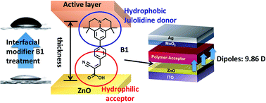
To enhance the performance of inverted polymer solar cells (PSCs), we have designed and synthesized interfacial modifiers (IMs) which provide better surface properties for the ZnO layer. The synthesized IMs were composed of electron donating and accepting parts. Julolidine or diethyl aniline was used as a donor part, and cyano acrylic acid as an acceptor part. The julolidine-based B1 material exhibited a much stronger dipole moment of 9.86 D than diethyl aniline-based B2 (9.17 D), and the water contact angle of the ZnO surface treated with B1 (65.3°) was much larger than that with B2 (39.8°). These julolidine effects were much more powerful than diethyl aniline: the julolidine moiety significantly decreased the hydrophilicity of the ZnO surface and its work function (WF). The inverted devices with the configuration of ITO/ZnO/IMs (B1 or B2)/PTB7-Th:PC71BM/MoO3/Ag were fabricated and the photovoltaic properties were investigated. Both B1 and B2 worked well as IMs, but B1-treated devices exhibited a much higher power conversion efficiency of 8.35% than B2-treated devices (7.80%). B1 treatment on ZnO effectively reduced series resistance and leakage current in the devices due to the julolidine effects. We believe that julolidine is an excellent electron donating building block for IMs in inverted PSCs and our approach can be applied to other IM systems universally to improve photovoltaic performance.
Introduction
Polymer solar cells (PSCs) are distinguished from inorganic solar cells due to their unique advantages of being light-weight, solution processable and flexible, and have been extensively studied for developing high-efficiency devices.1–4 Currently, polymer/[6,6]-phenyl-C71-butyric acid methyl ester (PC71BM) based bulk heterojunction devices have demonstrated over 10% power conversion efficiencies (PCE).5–7 PSCs can be classified as possessing either a conventional structure or an inverted architecture. The inverted device was designed to overcome the drawback of the normal structure consisting of ITO/poly(3,4-ethylene-dioxythiophene):poly(styrenesulfonate) (PEDOT:PSS)/active layer/Al. PEDOT:PSS is an excellent hole transporting material, but its acidity (pH 1–2) causes the chemical degradation of the ITO electrode, which is a serious problem for long term stability. In addition, low work function (WF) metals like calcium, barium or aluminium are easily oxidized under exposure to oxygen or water, resulting in fast degradation of the PCE.8,9 However, in the inverted structure, the low WF metals have been replaced by ITO doped with transparent oxides like zinc oxide or titanium dioxide. As an anode, air-stable high WF metals like Ag and Au have been applied. As a result, inverted device commonly showed the following configurations: ITO/cathode buffer layer/active layer/MoO3/Ag. Several cathode buffer materials have been developed: n-type metal oxides (e.g. ZnO and TiOx),10–13 transition metal chelates (e.g. titanium chelates and zirconium chelates)14,15 and alkali metal compounds (e.g. LiF, CsF and Cs2CO3).16 Among them, air-stable ZnO has been regarded as one of the promising candidates for the electron selective and hole blocking layer because of its high electron mobility, transmittance and solution processibility.10,11 However, there is a critical problem of ZnO layer in the inverted structure. One is that terminal hydroxyl groups of ZnO surface are working as the electron trapping and recombination sites.17 Another is that hydrophobic active layer can make poor contact with hydrophilic ZnO surface.18,19 To solve those issues, several polyelectrolytes having polar side chains20–23 or interfacial modifiers (IMs) containing carboxylic acid moiety24–29 are introduced on the ZnO surface. The design concept of those organic buffer materials is quite similar. Those materials contain both hydrophobic and hydrophilic parts: hydrophobic segment reduces surface tension with active layer, leading better interface quality, and the hydrophilic section can combine to ZnO surface. Importantly, when these organic buffers are connected to ZnO film, the dipole moment is generated from the ZnO surface. The strength of dipole moment of organic buffer is highly important to determine the WF of cathode. In case of conjugated polyelectrolytes, the number of quaternary or tertiary amine unit on the side chains is tuning the WF of ITO. Lee et al. reported that the effective WF of ITO is proportionally decreased by increasing the ionic density of polyelectrolytes.30 In case of IMs, their own dipole moment is directly affected on the WF of electrode. Wang et al. synthesized several organic IMs having different dipole moment and showed that the stronger dipole moments of IMs induced more upshifted WF of substrate.31 Moon et al. introduced (E)-2-cyano-3-{7-[4-(diphenylamino)phenyl]-10-hexyl-10H-phenothia-zine-3-yl}acrylic acid (PAPTA) as an IM and reported 18% improved PCE of 7.11%.32 There are several advantages of IMs. First, –COOH ended structure is covalently bonded to the ZnO layer, allowing the strong solvent resistance. Second, the surface energy, thickness, and dipole moment are easily tuned by chemical modification of conjugated structure.31 As shown in Fig. 1, hydrophobic part of IM changes the surface energy of ZnO film, the film thickness is determined by molecule length via the formation of self-assembled monolayer (SAM), and the dipole moments are controlled by the electron donating or accepting strength of molecules.
 |
| Fig. 1 Schematic diagram of the intramolecular charge transfer (ICT) of B1 and B2. Julolidine is much better electron donor than diethyl aniline moiety due to the structure and resonance effects. | |
Herein, we have synthesized B1 named (E)-2-cyano-3-(4-(1,1,7,7-tetramethyl-1,2,3,5,6,7-hexahydropyrido[3,2,1-ij]quinolin-9-yl)phenyl)acrylic acid containing julolidine as an electron donating moiety and B2 named (E)-2-cyano-3-(4′-(diethylamino)-[1,1′-biphenyl]-4-yl)acrylic acid having diethyl aniline as a donor part. As shown in Fig. 1, julolidine donor moiety destabilizes negative charge in intermediate states and promotes the fast charge transfer to the electron accepting cyano acrylic acid unit, resulting in strong intramolecular charge transfer (ICT) interaction. In addition, the cyclic structure of julolidine prevents the free rotation of amine unit, slightly promoting quinoid population.33–35 As a result, julolidine-based electron donor (D)–acceptor (A) structure induces highly efficient ICT interaction, leading narrower bandgap and higher dipole moment than diethyl aniline-based one.34,35 Using julolidine-based IM (B1), we successfully reduced WF and hydrophilicity of ZnO surface due to the strong dipoles of B1 and hydrophobic nature of julolidine. The inverted photovoltaic devices treated with B1 or B2 exhibited the enhanced device performance, but the B1-treated device showed further improved PCE of 8.35% compared to B2-based device (7.80%). The julolidine effects were discussed in terms of the optical and electrochemical properties, molecular energy levels and photovoltaic J–V characteristics.
Results and discussion
Synthesis and structural characterization
The synthetic approaches to IMs (B1 and B2) are described in Scheme 1 and their detail synthetic procedures are summarized in the ESI.† Compound 1 was synthesized via 2 steps from aniline, according to the literature procedure,36 and compound 2 was purchased from Sigma-Aldrich. Compound 3 (or 4) was synthesized via Suzuki coupling of compound 1 (or 2) and 4-(4,4,5,5-tetramethyl-1,3,2-dioxaborolan-2-yl)benzaldehyde. The final product B1 (or B2) was obtained by Knoevenagel condensation between compound 3 (or 4) and cyano acrylic acid. The diethyl aniline-based buffer B2 was synthesized to compare with the julolidine-based B1 material as an interfacial modifier. Matrix Assisted Laser Desorption Ionization Mass Spectrometer (MALDI-MS) showed that B1 and B2 have 440.44 and 321.47 Da, respectively, which identifies the final products.
 |
| Scheme 1 Synthetic routes of B1 and B2 and their MALDI mass spectra. | |
Optical and electrochemical properties
The absorption spectra of the B1 and B2 were measured in tetrahydrofuran (THF) solution and in films. The spectra are shown in Fig. 2(a) and summarized in Table 1. The absorption maxima (λmax) of B1 and B2 were 451 and 407 nm in solution, respectively, and 475 and 412 nm in film, respectively. B1 showed much red-shifted absorption spectra than B2 due to the more effective ICT interaction of B1 molecule. In addition, the absorption maximum of B1 in film was 24 nm more red-shifted than that of B1 in solution, but that of B2 in film showed just 7 nm bathochromic shift compared to that of B2 in solution. This indicates that the rotation forbidden amino site of julolidine promotes the molecular ordering in film states compared to the diethyl aniline unit. The optical band gaps (Eoptg) of B1 and B2 were determined from their absorption edges to be 2.05 and 2.34 eV, respectively.
 |
| Fig. 2 (a) Absorption spectra in solution and film state and (b) cyclic voltammograms of B1 and B2. | |
Table 1 Optical properties of the polymers
|
Solution |
Film |
p-Doping (V vs. Ag/Ag+) |
ELUMOe (eV) |
λmaxa (nm) |
λmaxb (nm) |
Eoptgc (eV) |
Eox/onset |
EHOMO,elecd (eV) |
Dilute solution in THF. Thin film on a quartz plate, formed by spin-coating a 1 wt% THF solution for 60 s at 1500 rpm. Bandgap calculated from the film-state absorption onset wavelength. HOMO energy level were determined from the Eonset of the first oxidation potential of ferrocene, −4.8 eV. The LUMO energy was estimated by adding the absorption onset to the HOMO energy. |
B1 |
451 |
475 |
2.05 |
0.30 |
−5.05 |
−3.00 |
B2 |
407 |
412 |
2.34 |
0.53 |
−5.28 |
−2.94 |
The highest occupied molecular orbital (HOMO) energy level (EHOMO) of B1 and B2 was verified by cyclic voltammetry (CV) and density functional theory (DFT) calculations (Table 1). The HOMO energy level of the synthesized molecules was calculated from CV measurements using the oxidation onset potentials relative to ferrocene as an internal standard, and their cyclic voltammograms are shown in Fig. 2(b). The onset oxidation potential (Eox) of B1 and B2 was 0.30 and 0.53 V, respectively, corresponding to HOMO energy levels of −5.05 and −5.28 eV, respectively. B1 exhibited relatively high-lying HOMO energy level compared to B2 due to the strong electron donating julolidine moiety. This result is in good agreement with the optical properties. The lowest unoccupied molecular orbital (LUMO) energy level (ELUMO) of B1 and B2 was estimated from the optical bandgap and the HOMO energy level, and calculated as −3.00 and −2.94 eV, respectively. LUMO energy levels of the two molecules are quite similar due to the identical electron accepting cyano acrylic acid.
The frontier orbitals of the B1 and B2 molecules were calculated using DMol3 package at DFT/B3LYP level and shown in Fig. 3. The HOMOs of two IMs showed a strong backbone contribution and electron delocalization along the entire molecules. In contrast, their LUMOs were largely localized on the electron withdrawing cyano acrylic acid unit. This confirms that they form D–A structures via ICT interactions between electron donating amino benzene unit and electron accepting cyano acrylic acid moiety.37 The calculated HOMO energy levels of B1 and B2 were −4.96 and −5.19 eV, respectively, and their LUMO levels were −2.25 and −2.33 eV, respectively. The two IMs having identical electron accepting moiety showed quite similar LUMO energy level because the electron density of LUMO was dominated on the electron accepting cyano acrylic acid unit. On the other hands, B1 containing julolidine donor has much higher HOMO energy level than B2 because the electron density of HOMO was well distributed on the electron donor. As a result, the simulated energy levels are quite similar trend with experimental results: B1 showed high-lying HOMO energy level and similar LUMO energy level with B2.38
 |
| Fig. 3 The ground-state (S0) geometric structure, and HOMO and LUMO orbitals of B1 and B2, calculated by DMol3 package at DFT/B3LYP level. | |
Work function tuning
The WF of ITO/ZnO layer with or without IMs was calculated from the high binding energy cutoff (Ecutoff) region of ultraviolet photoelectron spectroscopy (UPS) shown in Fig. S3.† The WF of ITO/ZnO electrode was measured to be 4.2 eV, but its WF was highly reduced as 3.84 eV (or 3.94 eV) after B1 (or B2) treatment.
It can be explained by interfacial dipole model. When the self-assembled monolayers (SAMs) of IMs were deposited on the top of ZnO electrode, the net dipoles of IMs induce a shift in the vacuum level at the surface of the IM-treated ZnO. In case of B1 and B2, the net dipoles were pointing out toward the active layer, thus the WFs of the electrodes were successfully reduced after the IM treatment. In addition, the net dipole moments of B1 and B2 were calculated to be 9.86 and 9.17 D, respectively, through the DFT calculation.
The strong electron donating julolidine moiety effectively enhanced dipole moment of B1 compared to the weak electron donating diethyl aniline donor on B2. As a result, the WF of ITO/ZnO electrode treated with B1 was further decreased compared to that with B2. We illustrated the energy diagram of the devices in the Fig. 4.
 |
| Fig. 4 Bandgap diagram of the fabricated inverted photovoltaic cells. The dashed line (---) indicates the energy levels by DFT calculation. | |
Photovoltaic properties
Bulk heterojunction photovoltaic devices were fabricated with the following configuration: ITO/ZnO/IMs/PTB7-Th:PC71BM/MoO3/Ag. The diluted IM solution (0.05 wt%) in THF was spin-coated onto the ZnO surface and washed with THF solution to remove unreacted IM residue. We confirmed the formation of IM layer on the ZnO film by X-ray photoelectron spectroscopy (XPS). The spectra with detailed characterization were shown in Fig. S4–S6.† The thickness of SAM was estimated to be 1.4 nm lower than 10 nm, quantum mechanical tunnelling limit. Thus, the permanent interfacial dipole from IM is the dominant mechanism for tuning the WF of ZnO surface.30 The J–V characteristics of the devices measured under an AM 1.5G solar simulator with a power density of 100 W cm−2 are shown in Fig. 5(a), and the corresponding photovoltaic parameters are summarized in Table 2. Without the IM layer, the device yielded a PCE of 7.18% with a Voc of 0.811 V, a Jsc of 15.30 mA cm−2, and a FF of 57.8%. When B1 showing strong dipole moment was applied to surface of ZnO, the device exhibited much enhanced PCE of 8.35% with a Jsc of 16.55 mA cm−2, and a FF of 62.0%. This result is also much better than the device treated with B2. As the WF of the IM-treated electrode was decreased, the series resistance (Rs) of the devices was gradually reduced and shunt resistance (Rsh) was highly enhanced. B1-treated devices showed the smallest electrode work function (3.84 eV), resulting in the lowest Rs of 2.15 Ω cm2 and one order of magnitude higher Rsh of around 106 Ω cm2. It is well-known that Rs value resulted from the resistance of the contacts between the active layer and the electrode, and Rsh from the leakage current providing an alternate current path for the light-generated current.39 As shown in Fig. 5(b), leakage current of the devices in the dark was significantly reduced after IM treatment. In addition, series resistance was also minimized at the B1-treated devices. Thus, the decrease in the WF of electrode successfully reduced the contact resistance and leakage current, resulting in better photovoltaic performance.
 |
| Fig. 5 The current density (J) versus voltage (V) characteristics of ZnO, ZnO/B1 and ZnO/B2 devices measured (a) under AM 1.5G simulated light illuminations with intensity of 100 mW cm−2 in air, and (b) in the dark. (c) J–V characteristics of the electron-only devices of those blend films. The mobilities are calculated by fitting the J–V curves in the SCLC regime. | |
Table 2 The device performance parameters of PTB7-Th:PC71BM solar cells depending buffer layer
Condition |
Voc (V) |
Jsc (mA cm−2) |
FF (%) |
PCE (%) |
SCLC mobilitya (cm2 V−1 s−1) |
Rshb (Ω cm2) |
Rsc (Ω cm2) |
Electron-only device of PTB7-Th/PC71BM blend films. Shunt resistance (Rsh). Series resistance (Rs) deduced from I–V curve in the dark. |
ZnO only |
0.811 ± 0.005 |
15.30 ± 0.15 |
57.8 ± 0.003 |
7.18 ± 0.0875 |
1.0 × 10⁻⁴ |
2.7 × 10⁵ |
3.35 |
ZnO + B1 |
0.816 ± 0.002 |
16.55 ± 0.15 |
62.0 ± 0.005 |
8.35 ± 0.066 |
1.5 × 10⁻⁴ |
2.3 × 10⁶ |
2.15 |
ZnO + B2 |
0.808 ± 0.003 |
15.78 ± 0.256 |
61.1 ± 0.002 |
7.80 ± 0.16 |
1.1 × 10⁻⁴ |
3.8 × 10⁶ |
2.49 |
The electron mobilities (μelectron) are measured with structures of ITO/ZnO/IMs or not/PTB7-Th:PC71BM (1
:
1.5 w/w, 3 vol% DIO)/LiF/Al by the steady-state space-charge limited current (SCLC) technique, and shown in Fig. 5(c) and S5.† IM-treated devices enhanced SCLC mobility compared to the device without IMs. In particular, the electron mobility of the B1-treated devices (1.5 × 10⁻⁴ cm2 V−1 s−1) was much higher than that of B2-treated devices (1.1 × 10⁻⁴ cm2 V−1 s−1). The better electron mobility of B1-treated devices contributes to the higher Jsc values in photovoltaic devices due to the enhanced charge carrier movement.
Another role of IMs is the modification of hydrophilic ZnO surface. The change of WF on ZnO generally effects on Voc of devices, but, in our study, the Voc value before and after IM treatment did not changed. Thus, the surface modification effect of IMs is also considered as an important factor. After treatment of IMs on ZnO film, the hydrophobicity of ZnO surface was significantly enhanced as shown in Fig. 6. In particular, B1-treated film showed the highest water contact angle of 65.3° with smallest surface tension of 49.9 mN m−1. Compared to B2-treated film, julolidine-based B1 film showed 25.5° higher water contact angle and 10.7 mN m−1 lower surface tension. Through the simple modification of the diethyl aniline to julolidine, we effectively modified ZnO surface to make better contact with hydrophobic active layer. Thus, the introduction of julolidine moiety in the IM is powerful strategy for enhancing the hydrophobicity of the metal oxide surface. The surface characteristics are summarized in Table 3.
 |
| Fig. 6 Water contact angle test of (a) ZnO, (b) ZnO/B1 and (c) ZnO/B2 film surface. | |
Table 3 Contact angle and surface tension value
|
DIa (°) |
CH2I2b (°) |
Polar (mN m−1) |
Disp. (mN m−1) |
Surface tension (mN m−1) |
Water contact angle. Diiodomethane contact angle. |
ZnO |
26.7 |
37.5 |
36.6 |
30.1 |
66.8 |
ZnO + B1 |
65.3 |
25.7 |
9.39 |
40.5 |
49.9 |
ZnO + B2 |
39.8 |
33.8 |
27.5 |
33.1 |
60.6 |
Overall, the better contact properties at the interfaces of ZnO and active layer by introduction of IMs successfully reduced Rs and enhanced Rsh and Jsc, resulting in the enhanced photovoltaic performance, which are mainly caused by the reduced surface tension of ZnO film and decreased WF of ZnO.
Conclusions
We have synthesized IMs (B1 and B2) and applied on the top of ZnO surface to enhance the interfacial contact with active layer and to tune the WF of electrode. B1 containing julolidine unit showed much higher net dipole moment than B2 having diethyl aniline because julolidine moiety has much stronger electron donating properties than diethyl aniline. Due to the stronger dipole moment, B1 effectively decreased the WF of ITO/ZnO electrode, resulting in the effective reduction of the series resistance in the photovoltaic devices. In addition, B1 significantly enhanced hydrophobicity of the ZnO surface, resulting in the better contact with hydrophobic active layer. As a result, PTB7-Th/PC71BM device treated with B1 exhibited highly improved PCE of 8.35% compared to the devices without IM (7.18%). We first introduced julolidine-based IM on the ZnO film to modify the surface characteristics for improving PSC performance. We demonstrate that julolidine has simple structure but is excellent electron donating unit for the design of D–A type IMs in the inverted PSCs.
Experimental section
Measurements
1H NMR and 13C NMR spectra were recorded on a Bruker Ascend™-400 spectrometer, with tetramethylsilane as an internal reference. Matrix-assisted laser desorption ionization time-of-flight (MALDI-TOF) mass spectra were obtained on a Bruker Autoflex Speed TOF/TOF instrument with dithranol as the matrix. The absorption spectra were measured on a SHIMADZU/UV-2550 model UV-visible spectrophotometer. Cyclic voltammetry was performed on a BAS 100B/W electrochemical analyzer with a three-electrode cell in a 0.1 N Bu4NBF4 solution in acetonitrile at a scan rate of 50 mV s−1. A film of each polymer was coated onto a Pt wire electrode by dipping the electrode into a polymer solution in chloroform. All measurements were calibrated against an internal standard of ferrocene (Fc), the ionization potential (IP) value of which is −4.8 eV for the Fc/Fc+ redox system. Atomic force microscopy (AFM) was measured by using tapping mode and AFM scan images (2 μm × 2 μm) were achieved in tapping mode on Nanoscope from Bruker. Contact angle and surface tension value were measured by phoenix 300 from SEO. co. Ltd using DI and diiodomethane.
Ultraviolet photoelectron spectroscopy (UPS)
A set of samples were analyzed using the AXIS Ultra DLD model (KRATOS inc.) in Korea Basic Science Institute (KBSI), Daejeon. The He I (21.2 eV) emission line was employed as a UV source. The helium pressure in the analysis chamber during analysis was about 4.0 × 10⁻⁸ Torr. The WF was determined using the incident photon energy, hν = 21.2 eV, Ecutoff, and Eonset.
Fabrication of photovoltaic devices
The photovoltaic devices were fabricated with the ITO/ZnO/IMs/PTB7-Th:PC71BM/MoO3/Ag structure. The ITO surface was cleaned by sonication and rinsing in distilled H2O, acetone, and isopropanol. An electron transporting ZnO layer (30 nm) was spin-coated onto each ITO substrate, and then IMs (0.05 wt%) in THF were spin-coated at 4000 rpm for 30 s on ZnO layer. We provided a control experiment in the ESI (Fig. S7 and Table S1†). The polymer solution for active layer was prepared by dissolving the polymer (12 mg mL−1) with PC71BM in chlorobenzene
:
DIO (97
:
3 v/v%). The PTB7-Th:PC71BM blended solutions were spin-coated onto the IM-treated ZnO layer. MoO3 and Ag were deposited sequentially under the vacuum pressure of <3 × 10⁻⁶ Torr, resulting in an active area of 0.09 cm2. The thickness of the active layer was measured using a KLA Tencor Alpha-step IQ surface profilometer. The current density–voltage (J–V) characteristics of the photovoltaic cells were determined by illuminating the cells with simulated solar light (AM 1.5G) at an intensity of 100 mW cm−2 using an Oriel 1000 W solar simulator. The electronic data were recorded using a Keithley 236 source-measure unit. The measurements were carried out after masking all but the active cell area of the fabricated device. All of the characterizations were carried out under ambient conditions. The illumination intensity was calibrated using a standard Si photodiode detector acquired from PV Measurements Inc., which was calibrated at the National Renewable Energy Laboratory (NREL). The EQE was measured as a function of wavelength under ambient conditions in the range of 300–900 nm using a xenon short arc lamp as the light source (McScience K3100 EQX). Calibration was performed using a Si reference photodiode.
Mobility measurements
Mobility measurements of PTB7-Th/PC71BM (w/w, 1
:
1.5) blend were done by a charge-only space-charge limited current (SCLC) method with the following diode structures: ITO/ETL/active layer/LiF/Al for electron-only devices by taking current–voltage measurements and fitting the results to a space-charge limited form. The electron mobility was calculated using the SCLC model, where the SCLC is described by J = 9ε0εrμV2/8L3, where J is the current density, L is the film thickness of the active layer, μ is the hole or electron mobility, εr is the relative dielectric constant of the transport medium, ε0 is the permittivity of free space (8.85 × 10⁻¹² F m−1), V is the internal voltage in the device, and V = Vappl − Vr − Vbi, where Vappl is the applied voltage to the device, Vr is the voltage drop due to contact resistance and series resistance between the electrodes, and Vbi is the built-in voltage due to the relative work function difference of the two electrodes.
Acknowledgements
This work was supported by the New & Renewable Energy Core Technology Program of the Korea Institute of Energy Technology Evaluation and Planning (KETEP), granted financial resource from the Ministry of Trade, Industry & Energy, Republic of Korea. (20143010011890).
Notes and references
- C. J. Brabec, N. S. Sariciftci and J. C. Hummelen, Adv. Funct. Mater., 2001, 11, 15–26 CrossRef CAS.
- S. Günes, H. Neugebauer and N. S. Sariciftci, Chem. Rev., 2007, 107, 1324–1338 CrossRef PubMed.
- M. Helgesen, R. Sondergaard and F. C. Krebs, J. Mater. Chem., 2010, 20, 36–60 RSC.
- B. Zhao, Z. He, X. Cheng, D. Qin, M. Yun, M. Wang, X. Huang, J. Wu, H. Wu and Y. Cao, J. Mater. Chem. C, 2014, 2, 5077–5082 RSC.
- Y. Liu, J. Zhao, Z. Li, C. Mu, W. Ma, H. Hu, K. Jiang, H. Lin, H. Ade and H. Yan, Nat. Commun., 2014, 5, 5293 CrossRef CAS PubMed.
- C. Liu, C. Yi, K. Wang, Y. Yang, R. S. Bhatta, M. Tsige, S. Xiao and X. Gong, ACS Appl. Mater. Interfaces, 2015, 7, 4928–4935 CAS.
- V. Vohra, K. Kawashima, T. Kakara, T. Koganezawa, I. Osaka, K. Takimiya and H. Murata, Nat. Photonics, 2015, 9, 403–408 CrossRef CAS.
- M. Jørgensen, K. Norrman and F. C. Krebs, Sol. Energy Mater. Sol. Cells, 2008, 92, 686–714 CrossRef.
- E. Voroshazi, B. Verreet, A. Buri, R. Müller, D. Di Nuzzo and P. Heremans, Org. Electron., 2011, 12, 736–744 CrossRef CAS.
- K. Zilberberg, J. Meyer and T. Riedl, J. Mater. Chem. C, 2013, 1, 4796–4815 RSC.
- S. Kim, C.-H. Kim, S. K. Lee, J.-H. Jeong, J. Lee, S.-H. Jin, W. S. Shin, C. E. Song, J.-H. Choi and J.-R. Jeong, Chem. Commun., 2013, 49, 6033–6035 RSC.
- Z. Yin, Q. Zheng, S.-C. Chen, D. Cai, L. Zhou and J. Zhang, Adv. Energy Mater., 2014, 4, 1301404 Search PubMed.
- C. Jiang, R. R. Lunt, P. M. Duxbury and P. P. Zhang, RSC Adv., 2014, 4, 3604–3610 RSC.
- Z. A. Tan, C. Yang, E. Zhou, X. Wang and Y. Li, Appl. Phys. Lett., 2007, 91, 023509 CrossRef.
- Z. A. Tan, S. Li, F. Wang, D. Qian, J. Lin, J. Hou and Y. Li, Sci. Rep., 2014, 4, 4691 Search PubMed.
- L. Yang, H. Xu, H. Tian, S. Yin and F. Zhang, Sol. Energy Mater. Sol. Cells, 2010, 94, 1831–1834 CrossRef CAS.
- I. Litzov and C. J. Brabec, Materials, 2013, 6, 5796–5820 CrossRef.
- R. Lampande, G. W. Kim, R. Pode and J. H. Kwon, RSC Adv., 2014, 4, 49855–49860 RSC.
- S. H. Eom, M.-J. Baek, H. Park, L. Yan, S. Liu, W. You and S.-H. Lee, ACS Appl. Mater. Interfaces, 2014, 6, 803–810 CAS.
- Y.-M. Chang and C.-Y. Leu, J. Mater. Chem. A, 2013, 1, 6446–6451 CAS.
- T. Yang, M. Wang, C. Duan, X. Hu, L. Huang, J. Peng, F. Huang and X. Gong, Energy Environ. Sci., 2012, 5, 8208–8214 CAS.
- A. K. K. Kyaw, D. H. Wang, V. Gupta, J. Zhang, S. Chand, G. C. Bazan and A. J. Heeger, Adv. Mater., 2013, 25, 2397–2402 CrossRef CAS PubMed.
- C. Duan, K. Zhang, C. Zhong, F. Huang and Y. Cao, Chem. Soc. Rev., 2013, 42, 9071–9104 RSC.
- Y. Shi, L. Tan, L. Chen and Y. Chen, Phys. Chem. Chem. Phys., 2015, 17, 3637–3646 RSC.
- Y. E. Ha, M. Y. Jo, J. Park, Y.-C. Kang, S. I. Yoo and J. H. Kim, J. Phys. Chem. C, 2013, 117, 2646–2652 CAS.
- H.-L. Yip, S. K. Hau, N. S. Baek, H. Ma and A. K. Y. Jen, Adv. Mater., 2008, 20, 2376–2382 CrossRef CAS.
- R. Po, C. Carbonera, A. Bernardi and N. Camaioni, Energy Environ. Sci., 2011, 4, 285–310 CAS.
- C. Yi, K. Yue, W.-B. Zhang, X. Lu, J. Hou, Y. Li, L. Huang, G. R. Newkome, S. Z. D. Cheng and X. Gong, ACS Appl. Mater. Interfaces, 2014, 6, 14189–14195 CAS.
- L. Hu, L. Chen, X. Hu and Y. Chen, J. Mater. Chem. C, 2014, 2, 10282–10290 RSC.
- B. H. Lee, I. H. Jung, H. Y. Woo, H.-K. Shim, G. Kim and K. Lee, Adv. Funct. Mater., 2014, 24, 1100–1108 CrossRef CAS.
- J. Yu, T.-L. Shen, W.-H. Weng, Y.-C. Huang, C.-I. Huang, W.-F. Su, S.-P. Rwei, K.-C. Ho and L. Wang, Adv. Energy Mater., 2012, 2, 245–252 CrossRef CAS.
- C. E. Song, K. Y. Ryu, S.-J. Hong, C. Bathula, S. K. Lee, W. S. Shin, J.-C. Lee, S. K. Choi, J. H. Kim and S.-J. Moon, ChemSusChem, 2013, 6, 1445–1454 CrossRef CAS PubMed.
- Y. Yang, F. Liu, H. Wang, M. Zhang, H. Xu, S. Bo, J. Liu, L. Qiu, Z. Zhen and X. Liu, Phys. Chem. Chem. Phys., 2014, 16, 20209–20215 RSC.
- J. V. Lockard, A. Butler Ricks, D. T. Co and M. R. Wasielewski, J. Phys. Chem. Lett., 2010, 1, 215–218 CrossRef CAS.
- H. Choi, J. K. Lee, K. H. Song, K. Song, S. O. Kang and J. Ko, Tetrahedron, 2007, 63, 1553–1559 CrossRef CAS.
- H. K. Ju, J. S. Lim, C. Lee, D. H. Choi and D. W. Kim, Mol. Cryst. Liq. Cryst., 2008, 491, 152–163 CrossRef CAS.
- I. H. Jung, J.-H. Kim, S. Y. Nam, C. Lee, D.-H. Hwang and S. C. Yoon, Macromolecules, 2015, 48, 5213–5221 CrossRef CAS.
- I. H. Jung, D. Zhao, J. Jang, W. Chen, E. S. Landry, L. Lu, D. V. Talapin and L. Yu, Chem. Mater., 2015, 27, 5941–5948 CrossRef CAS.
- H. I. Kim, T. T. T. Bui, G.-W. Kim, G. Kang, W. S. Shin and T. Park, ACS Appl. Mater. Interfaces, 2014, 6, 15875–15880 CAS.
Footnote |
† Electronic supplementary information (ESI) available: The detailed synthetic procedures, MALDI-MS spectra, EQE and SCLC spectra, and AFM images. See DOI: 10.1039/c5ra21087a |
|
This journal is © The Royal Society of Chemistry 2015 |
Click here to see how this site uses Cookies. View our privacy policy here.