DOI:
10.1039/C5RA21026G
(Paper)
RSC Adv., 2016,
6, 3642-3649
Giant UV-sensitivity of ion beam irradiated nanocrystalline CdS thin films
Received
10th October 2015
, Accepted 12th November 2015
First published on 16th November 2015
Abstract
A highly sensitive UV-detector is devised for the first time from ion beam irradiated nanocrystalline CdS (nc-CdS) thin films. The UV-sensors are fabricated using pulsed laser deposited nc-CdS thin films on Si wafer and subsequent irradiation treatment. Swift heavy ion irradiation (SHII) of the nc-CdS thin films is carried out using 70 MeV 58Ni6+ ions. The sensors used in the present study are easy to fabricate and require inexpensive materials; they feature characteristics similar to those of UV sensors designed with complex structures and expensive procedures. Current–voltage (I–V) measurements reveal an enrichment in carrier concentration and improvement in conductivity after exposure to SHII. This giant conductivity may be attributed to an enhancement in sulfur vacancies as a consequence of SHII. The sensor exhibits improvements in the responsivity, photosensitivity, and efficiency as a function of the ion fluence and attains maximum values of ∼53 W A−1, 576.4% and 15.6 × 10³% respectively for a film irradiated at a fluence of 1 × 10¹³ ions per cm2. The response time of the sensor reduces with the increase in ion fluence and reaches a minimum of a rise time of 165 ms and fall time of 65 ms at 3 V for these sensors. A possible mechanism involved in the SHII induced moderation of conductivity and consequently photosensitivity is explained on the basis of variation in the defect densities.
Introduction
Over the past two decades, one-, two-, three- and zero-dimensional semiconductor nanostructures (SNs) have been serving as model materials to help us understand basic physical phenomena at nano-dimensions and for the fabrication of nanoscale devices including solar cells, nanolasers, light emitting diodes (LEDs), and photodetectors with improved performance and operating conditions.1 SNs are believed to be excellent building blocks for the next generation of highly sensitive and selective sensors because of their high surface-to-volume ratio and multifunctionality.2 Immense efforts have been made in the advancement of photosensors, owing to the diverse applications of photodetectors as binary switches in imaging techniques, light-wave communications, as well as in future memory storage and optoelectronic circuits in which the operation is based on the measurement of their optoelectronic response to incident radiation.3 Particularly, the detection of ultra-violet (UV) radiation out of all the electromagnetic spectrum has attracted superfluous attention because of its primary employment in many commercial, military and scientific areas such as ozone layer monitoring, flame detection, missile warning systems, medicine, astronomy, and UV based skin therapies etc.4 Out of all three categorized UV (UV-A, B and C) wavelengths, overexposure to UV-A radiation is the most hazardous for living beings. Furthermore, exposure to UV radiation leads to erythema, premature aging and skin pigmentation.5 Still, microelectronic industries require the use of UV-A (λ = 400–320 nm) radiation for patterning. Therefore, the development of efficient, stable and high-speed ultraviolet (UV) photodetectors is of the utmost importance.
Till date, a number of SNs have been used in UV-detectors and the mechanism involved in the photodetection has also been uncovered to some extent.3–17 Cadmium sulfide (CdS) with its direct band gap (for bulk CdS ∼ 2.42 eV) is one of the most studied metal chalcogenide semiconductors because of its relatively low work function, large refractive index, outstanding emission in the visible range, and excellent thermal and chemical stability. The excellent electronic and optical properties of CdS have been exploited for the development of solar cells,18 LEDs,19 photodetectors,8,9 waveguides,20 electrochemiluminescence sensors,21 bio-imaging,22 and lasers.23 Diverse approaches have been applied to improve the photoconductivity and thereby UV-sensitivity of SNs including composition and band gap engineering,1,6 formation of alloy layers,9,10 field effect transistors,1,6,11 impurity incorporation,24 piezo-phototronics,25 formation of a heterostructure,25,26 formation of Schottky contacts12 etc. However, there has been negligible interest in the influence of post deposition treatments viz. annealing and swift heavy ion irradiation (SHII) on the modification of photosensing materials and devices. Recently, Shaikh et al.27 studied the current voltage (I–V) characteristics of a 250 °C annealed CdS–Bi2S3 bi-layer thin film and a film irradiated by 120 MeV Au9+ ions at a particular fluence of 5 × 10¹² ions per cm2 under white light illumination. They obtained 28% photosensitivity for the irradiated film. However, systematic studies of using SHII with varying fluence to induce material modifications for photodetection have rarely been performed. Here, it is notable that the scope of ion beam induced multifunctionality has been extended for diverse applications including gas sensing,28 photodiodes,29 thermoelectricity30 along with material engineering and characterization in recent years. The underlying consequences of SHII such as defect engineering,31,32 nanostructure formation,33 crystal lattice engineering,34,35 high pressure phase generation36 etc. are responsible for these advancements. SHII leads to many fold advantages over conventional thermal annealing/laser annealing/rapid thermal annealing as; (1) the particle size can be tailored depending on the ion beam parameters, (2) one can control the defects (creation/annihilation) in a precise way by selecting ion beam parameters, (3) SHII avoids the possibility of interdiffusion of elements at the material/substrate interface, which usually occurs in the post deposition annealing at elevated temperature, (4) the spatial selectivity (longitudinal as well as lateral) of range of ions in matter i.e. controlled depth profiling and distribution. Since SHII can provide a vast range of modifications in the materials, it is a promising tool for establishing new horizons in designing and fabricating futuristic devices and moderating their performances.
In this article, we have extended the application of SHII to improve the UV sensitivity of nanocrystalline CdS (nc-CdS) thin film sensors in a systematic way for the first time. For this purpose, pulsed laser deposited (PLD) nc-CdS thin films were irradiated with different fluences of 70 MeV Ni ions followed by UV sensing studies at 355 nm laser illumination. Here, we have demonstrated that SHII causes an increment in the carrier concentration, which enhances the current and photocurrent with improved photosensitivity. The mechanism involved in the carrier concentration enhancement under the influence of SHII is discussed considering the defect density concentration as an impact of SHII.
Experimental section
Thin film deposition
The detailed procedure for the growth of the nc-CdS thin films by PLD is described elsewhere.32 All the samples investigated were synthesized using PLD by guiding a pulsed excimer KrF laser – an ultraviolet source of 248 nm emission – onto a target of chemically synthesized CdS quantum dots (QDs).37 A laser beam of an energy of 300 mJ per pulse with a repetition rate of 10 Hz and a pulse width of 10 ns was focused onto a rotating target which was kept at a distance of 5.5 cm from an n-type single-crystal Si (111) wafer of size 1 × 1 cm2 and mounted at an oblique angle of 30° with respect to the incident laser beam. Films were deposited, keeping the substrate at 200 °C inside a stainless steel vacuum chamber while maintaining base pressure higher than 5 × 10⁻⁶ Torr. The thickness of the films was ∼ 250 nm.
Swift heavy ion irradiation
To examine the ion beam induced functionality in nc-CdS thin films, irradiation was carried out at different fluences (1 × 10¹² to 1 × 10¹⁴ ions per cm2) of 70 MeV Ni6+ ions using a 15 UD Pelletron Accelerator at the Inter-University Accelerator Centre (IUAC), New Delhi, India. The SHII was performed inside a chamber with a base pressure of ∼2 × 10⁻⁶ Torr at room temperature. The ion beam of an approximately constant current of ∼1 pnA (particle nano Ampere) was scanned over the entire area of film (∼1 × 1 cm2) with an electromagnetic scanner to ensure uniform irradiation. The electronic energy loss, nuclear energy loss, and range of the incident 70 MeV Ni ions for CdS were calculated using electronic stopping, nuclear stopping and range of ions in matter (SRIM) methods,38 and found to be 10.58 keV nm−1, 0.031 keV nm−1 and 10.94 μm, respectively.
Characterization
The basic characterization (glancing angle X-ray diffraction, micro-Raman, transmission electron microscopy (TEM), UV-visible and photoluminescence (PL) spectroscopy) for structural and optical studies was carried out and the methods are reported elsewhere.32 In this study, Hall measurements were carried out to study the carrier concentration, conductivity, mobility and nature of the majority charge carriers using an ECOPIA-HMS-3000 operating at a magnetic field of 0.57 T. To study the surface morphology and grain size, atomic force microscopy (AFM) was carried out using a Nanoscope IIIa SPM Atomic Force microscope in tapping mode.
UV-sensing measurements
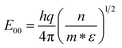
For the UV sensing, a metal–semiconductor–metal (M–S–M) structure was employed with symmetric geometry for the pristine and irradiated films using high quality Ag paste. The I–V characteristics of the nc-CdS thin film structures were measured in the voltage range of −5 V to +5 V under illumination with an UV laser of power 1 mW and wavelength 355 nm or under dark conditions in ambient air at room temperature using a semiconductor characterization system (Keithley 4200 SCS). The time-dependent photocurrent response under UV laser illumination for the light-on and light-off states was recorded at applied voltages ranging from 1 V to 5 V.
Results and discussion
The surface morphology, root mean square (rms) surface roughness and average particle size (APS) of the pristine and irradiated films were investigated using AFM. Fig. 1a and b show the two-dimensional micrographs (at 0.5 μm × 0.5 μm scale) of the pristine film and the film irradiated at fluence of 1 × 10¹³ ions per cm2 respectively. It is evident that the pristine film is comparatively porous with respect to the irradiated one. The irradiated films are uniform, continuous and contain well-distinguished small particles. The corresponding particle size histograms are shown in the insets of each micrograph. The APS and rms roughness of the pristine film are ∼9.4 nm and ∼4.9 nm respectively (Fig. 1a). It was observed that the APS and rms roughness decrease with the increase in the ion fluence up to 1 × 10¹³ ions per cm2, and then increase for the highest fluence used. The rms roughness values were estimated as ∼3.2 nm, 2.1 nm and 3.1 nm for the films irradiated at a fluence of 1 × 10¹² ions per cm2, 1 × 10¹³ ions per cm2, and 1 × 10¹⁴ ions per cm2 respectively. UV-visible absorption spectroscopy was carried out to study the band gap modifications in the nc-CdS films as an impact of SHII. Fig. 1c shows the variation of APS estimated using effective mass approximation employing the band gaps determined using UV-visible spectroscopy along with the APS estimated using AFM. It illustrates that the estimated values of APS using the two methods are very close and follow the same trend. Approximately the same APS as from the AFM for the 1 × 10¹³ ions per cm2 irradiated film can be viewed from the transmission electron micrograph (Fig. 1d).
 |
| | Fig. 1 AFM micrographs at a 0.5 μm × 0.5 μm scale of the (a) pristine film and (b) film irradiated at a fluence of 1 × 10¹³ ions per cm2, (c) average particle size estimated using the AFM images and UV-visible spectroscopy, and (d) TEM image of the 1 × 10¹³ ions per cm2 irradiated film (insets: corresponding particle size distribution histograms). | |
To investigate the variation in the electrical transport parameters as an impact of SHII, Hall measurements were carried out. The different parameters obtained from the Hall measurements are summarized in Table 1.
Table 1 Parameters obtained by Hall measurementa
| Sample |
RH |
μ cm2 V−1 S−1 |
σ mho m−1 |
n cm−3 |
| RH = Hall coefficient, μ = mobility, σ = conductivity, and n = carrier concentration. |
| Pristine |
−5.27 |
317.1 |
60.16 |
1.18 × 10¹⁸ |
| Irradiated at 1 × 10¹² ions per cm2 |
−3.592 |
284.1 |
79.06 |
1.74 × 10¹⁸ |
| Irradiated at 1 × 10¹³ ions per cm2 |
−1.216 |
193.4 |
159.04 |
5.14 × 10¹⁸ |
| Irradiated at 1 × 10¹⁴ ions per cm2 |
−1.534 |
207.7 |
135.39 |
4.07 × 10¹⁸ |
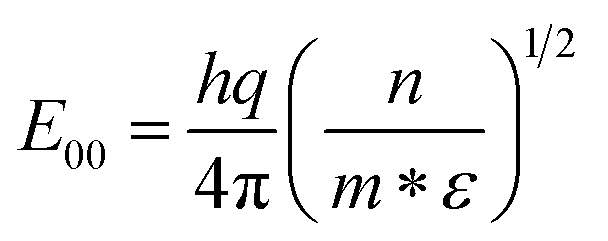
It was noticed that the Hall coefficient of all the films is negative, suggesting that the concentration of electrons is higher than the holes i.e. the films are n-type. It is obvious that the electrical resistivity reduces and the carrier (electron) concentration increases as a function of irradiation fluence up to 1 × 10¹³ ions per cm2, beyond this fluence, these two parameters show the opposite behavior. The electron concentration for the pristine sample and the 1 × 10¹² ions per cm2, 1 × 10¹³ ions per cm2, and 1 × 10¹⁴ ions per cm2 irradiated samples was estimated as 1.18 × 10¹⁸, 1.74 × 10¹⁸, 5.14 × 10¹⁸, and 4.07 × 1018 cm−3 respectively. The reduction in electron mobility upon irradiation, up to 1 × 10¹³ ions per cm2, is due to a rise in the defect concentration as a consequence of atomic displacement of the Cd or S atoms at substitutional or interstitial sites. Fig. 2a, b and c show the unirradiated film, the film under exposure to irradiation and different possible phenomena during the passage of SHI through the material, respectively. The schematic in Fig. 2c shows only some structural alteration phenomena relevant here out of many complex phenomena. It can be seen that there is always a prominent chance of the creation of vacancies and interstitial sites by displacement of atoms during the passage of SHI through the material. The increase in defect density results in enhancement of the inter-collision of charge carriers and thus reduces the mobility of the carriers.39 A schematic of the fabricated sensor is shown in Fig. 2d.
 |
| | Fig. 2 Schematic of (a) the pristine film, (b) the film under exposure to SHII, (c) various promising phenomena as a consequence of passage of SHI through the material and (d) the sensor. | |
I–V characteristics of all the samples under dark and UV light illumination conditions are shown in Fig. 3a–d. It is clear that the current rises with increase of the ion fluence and becomes maximum at an irradiation fluence of 1 × 10¹³ ions per cm2. The maximum change observed in the current, for the 1 × 10¹³ ions per cm2 irradiated sample at 5 V, is more than an order of magnitude with respect to the pristine film. It is evident that the I–V characteristics show nearly Schottky behavior. For a Schottky diode, the total current (I) across a metal–semiconductor junction is represented as:40
| |
 | (1) |
where
J is the current density through the barriers,
A is the contact area associated with barrier, and
JA is a slowly varying function of the applied bias voltage.
E0 is provided by
| |
 | (2) |
where
E00 is a function of the carrier concentration (
n) and is defined as
| |
 | (3) |
where
m* is the effective mass of an electron and
ε is the dielectric constant. The Schottky behavior of the
I–
V characteristics was studied by fitting the experimental data with the above equation and estimating the electron concentration. The electron concentration for the pristine, and 1 × 10
12 ions per cm
2, 1 × 10
13 ions per cm
2, and 1 × 10
14 ions per cm
2 irradiated samples was calculated as 1.13 × 10
18, 1.62 × 10
18, 3.73 × 10
18, and 3.11 × 10
18 cm
−3 respectively. It is significant to mention here that the electron concentration estimated using the above equation is consistent with the value obtained from the Hall measurements for the pristine and 1 × 10
12 ions per cm
2 irradiated samples. However, there is a perceptible divergence for the values of electron concentration for the other two samples. This is because of slight deviation of the
I–
V characteristics from Schottky behavior as a consequence of an increase in electron concentration. The enhancement in electron concentration as a function of ion fluence is ascribed to the rise in sulfur vacancies and thus conductance. Recently, we studied the variation of defect densities as a function of ion fluence and suggested that due to electronic activation as an impact of SHII, Cd and S atoms move from one minimum to the next lower minimum by crossing a potential barrier during recrystallization, which leads to enrichment of the population density of defects.
32 Since the displacement of a Cd atom to an interstitial position is easier than that of a S atom under high energy electronic bombardment,
41 at a lower irradiation fluence (1 × 10
12 ions per cm
2) the enhancement in the population density of sulfur vacancies (
Vs) is relatively very small compared to that at an irradiation fluence of 1 × 10
13 ions per cm
2, thereby resulting in the observed variation in conductance. In contrary, at a fluence of 1 × 10
14 ions per cm
2 it is predicted that the particle size further reduces, causing dissolution of smaller crystals and growth of larger particles due to Ostwald ripening.
42 The grain growth results in reduction of the surface to volume ratio and hence the population density of
Vs, which ultimately leads to a drop in the electron concentration and conductance.
 |
| | Fig. 3 Current–voltage (I–V) characteristics of the pristine and irradiated sensing devices under dark (black symbols) and UV-illumination (red symbols) conditions. | |
It is obvious from Fig. 3a–d that all the films show good UV sensitivity under illumination as the photocurrent of all the samples is higher than the respective dark current. It is manifested that the photocurrent increases by ∼2.3, 2.9, 6.3, and 4.0 times for the pristine, and 1 × 10¹² ions per cm2, 1 × 10¹³ ions per cm2, and 1 × 10¹⁴ ions per cm2 irradiated samples respectively relative to the respective dark current at 5 V. The mechanism responsible for the enhancement in photocurrent with respect to the dark current can be understood as follows. Since there is always a finite content of oxygen present on the surface of each sample due to adsorption of atmospheric oxygen, this leads to charged surface states on CdS from the transfer of conduction electrons to the adsorbed species. The transport of electrons generates a compensating space charge layer of ionized donors and a Schottky barrier is created. Under the illumination of UV-light free carriers are created. The free holes so created are forced to the surface by the barrier field, and these holes are neutralized by the negative ions to release the adsorbed gas. The photogenerated electrons are driven into the interior of the film by the barrier field enhancing the concentration of electrons in the conduction band and leading to a boost in conductivity.43 The entire mechanism of photoconduction can be interpreted as:
Next, the UV-response characteristics were investigated within the entire range of the applied bias voltage (1 V to 5 V). The time dependent UV-sensing at the lowest bias voltage of 1 V is shown for all the prepared sensors in Fig. 4a. Repeated cycles of the UV on/off modes are displayed in sequential manner. This divulges that the response of the different sensors to the incident light is fast and exhibits excellent stability and repeatability. Analytical investigation suggested a rise time (tr) of 1100 ms, 600 ms, 200 ms & 270 ms and a fall time (tf) of 986 ms, 820 ms, 72 ms & 95 ms for the pristine, and 1 × 10¹² ions per cm2, 1 × 10¹³ ions per cm2, and 1 × 10¹⁴ ions per cm2 irradiated UV-sensors respectively. However, the minimum response time is achieved at various bias voltages for the different sensing devices. Herein, only the response times of the different samples at the lowest bias voltage are mentioned. To calculate the rise and decay time constants (τr and τd), we tried to fit our experimental data to an equation with a single exponent of the type:24 I = I0 + Ce−t/τ. Fitting revealed that the above equation is unable to proffer a good fit for the rising edge, though it offers a good fit for the trailing edge of the experimental data as shown in Fig. 4b. Therefore, two exponents of the type: I = I0 + C1e−t/τ1 + C2e−t/τ2 with two time constants τ1 and τ2 corresponding to a shorter and longer time respectively were used to fit the rising edge. Here C1 and C2 are scaling constants and τ1 and τ2 are related to the charge generation and the diffusion of charge carriers respectively. Two time constants for the rising edge can be expected considering the porosity of the films, which was well visualized in AFM studies. It can be seen from Fig. 1 that the distribution of particles on the surface and the rms roughness of the pristine film are relatively greater than those of the irradiated films, indicating a relatively larger porosity of the pristine film, which results in adsorption of more oxygen on the surface of this film. This enhances the space charge region and built-in-potential near the surface, which blocks the generation of electron–hole pairs and thus a higher τ1 is observed. The reduced carrier concentration of this film leads to a higher rate of charge diffusion and thus τ2 is relatively small. We found that the rising edge of the experimental data is described well using this equation, as shown in the inset of Fig. 4b. The different parameters estimated from the data fitting are summarized in Table 2.
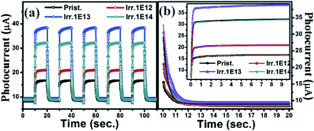 |
| | Fig. 4 (a) Time response of the UV-sensing devices at a bias voltage of 1 V. (b) Trailing edge fitted with I = I0 + Ce−t/τ. Inset: rising edge fitted with I = I0 + C1e−t/τ1 + C2e−t/τ2. | |
Table 2 The parameters calculated from fitting of the rising and trailing edges with the equations I = I0 + C1e−t/τ1 + C2e−t/τ2 and I = I0 + Ce−t/τ respectivelya
| Sample |
τ1 (ms) |
τ2 (s) |
τ (ms) |
| τ1 = rise time constant 1, τ2 = rise time constant 2, and τ = decay time constant. |
| Pristine |
117 ± 1 |
2.25 ± 0.17 |
748.1 ± 8 |
| Irradiated at 1 × 10¹² ions per cm2 |
109 ± 1 |
2.27 ± 0.07 |
719.9 ± 5 |
| Irradiated at 1 × 10¹³ ions per cm2 |
76 ± 0.5 |
5.72 ± 0.46 |
584.7 ± 4 |
| Irradiated at 1 × 10¹⁴ ions per cm2 |
95 ± 1 |
4.97 ± 0.53 |
594.5 ± 6 |
In order to evaluate the entire performance of the device, crucial parameters such as responsivity (R), external quantum efficiency (η), and sensitivity (S) were further calculated. Mathematically these parameters are defined as:5
| |
 | (6) |
where
Ip is the photocurrent,
Pin is the incident power,
h is Planck’s constant,
c is the velocity of light,
e is the electronic charge,
λ is the wavelength of the incident light, and
Id is the dark current.
and is the spectral responsivity. The values of all these parameters were calculated at different bias voltages ranging from 1 V to 5 V. The variation in responsivity is shown in
Fig. 5a, whereas the inset of
Fig. 5a shows variation in the external quantum efficiency as a function of bias voltage. It is evident that both the parameters show nearly linear behavior with bias voltage, and attain maximum values at 5 V for all the sensing devices. The highest obtained values of responsivity and quantum efficiency are ∼53 A W
−1 and 15.6 × 10
3% at 5 V for the 1 × 10
13 ions per cm
2 irradiated sensor. The sensitivity of the UV-sensing devices is shown in
Fig. 5b. This exemplifies that the maximum sensitivities for all the sensing devices were achieved at diverse bias voltages. The largest obtained value of sensitivity is ∼578.6% for the 1 × 10
13 ions per cm
2 irradiated sensor operating at 3 V, which is fairly high in the context of existing reports.
27
 |
| | Fig. 5 (a) Variation of responsivity as a function of bias voltage (inset: external quantum efficiency varying with bias voltage) and (b) photosensitivity of the various devices at different bias voltages. | |
The available literature on UV-sensors suggests that nc-CdS thin films are not much explored as a UV-sensitive material. However, a variety of ideas have been exploited to improve the performance of UV-sensors, e.g. fabrication using nanowires, nanobelts and nanosheets of CdS or other SNs. To the best of our knowledge the minimum response (rise and fall) time achieved by nc-CdS thin films is a few seconds, whereas it is a few tens of milliseconds in the case of CdS nanobelts. A brief comparison of various UV-sensing devices is presented in Table 3. A lot of work has been carried out employing ZnO thin films, nanostructures, composites or heterostructures for the development of UV-sensors. However, the sensitivity, response time and lower operating voltages have been the major issues and a challenge for researchers exploring other materials as a means to fabricate highly sensitive and faster devices for real time applications. Thiyagarajan et al. investigated artificially introduced defects on a graphene surface for the fabrication of a gate tunable UV-sensor and achieved a response time in the order of seconds.11 A wide wavelength photodetector exhibiting fairly sensitive behavior for UV-light was demonstrated by Ali et al. using indium selenide microwires grown using a vapor-solid technique.13 Shao et al. fabricated an organic–inorganic hybrid structure to realize an UV-sensor with a sufficiently reduced response time.14 A highly selective, visible light-blind UV-A sensor was devised by Kobayashi et al. by growing MgCdS/ZnCdS short period superlattice structures using a molecular beam epitaxy method.10 A positive step towards highly responsive and extremely efficient UV-sensors was realized by Zhang et al. using carbon-fiber/ZnO–CdS double shell microwires with a lower applied bias of 2 V.25 In a recent report by Lin et al., a UV-sensor of exceptional responsivity (∼105) and detectivity (∼1016 Jones) at 1 V under an illumination of just 3.5 pW was demonstrated. The sensor can be operated at a bias voltage as low as 1 mV with a remarkable response.16 Nevertheless, for most of the reports where a high sensitivity/efficiency or a lower response time/bias voltage were achieved, the device fabrication involves intricate structures that require tedious steps. In contrary, the UV-sensors presented herein are in the intermediate range as far as the various parameters are concerned along with an easy-to-prepare fabrication. The overall performance of the presented sensing devices is better than for most of the reports on nc-CdS thin films,27,44 some 1D or 2D CdS nanostructures2,12,15,17 and even better than in a recent report on branched CdS/ZnO heterostructure26 based devices. Conclusively, the sensors proposed here are easy to fabricate and require inexpensive materials, the feature characteristics being similar to those of UV sensors made with complex and expensive procedures. The present study has aimed to explore SHII treatment of thin films to enhance the performance of sensing devices by defect engineering and suggests that incorporating post deposition treatment (SHII) alongside intricate fabrication routes can further moderate the performance of photosensing devices. Further experiments with different ion beam parameters may lead to astonishing improvements for UV-sensing device scenarios.
Table 3 Comparison of the photoelectrical parameters of different CdS photosensing structuresa
| CdS NSs |
Bias voltage (V) |
λ (nm) |
τr (ms) |
τf (ms) |
Sensitivity/responsivity |
η (%) |
Reference |
| λ = wavelength of the illuminating light, τr = rise time, τf = fall time and η = quantum efficiency. |
| CdS single nanoribbons |
1 |
360 |
— |
— |
27% |
— |
2 |
| ZnO spherical particles |
10 |
330 |
— |
— |
350% |
— |
3 |
| Zn1−xMgxO films |
1 |
360 |
— |
— |
0.22 A W−1 |
— |
6 |
| ZnO NWs/graphene |
8 |
365 |
9500 |
38![[thin space (1/6-em)]](https://www.rsc.org/images/entities/char_2009.gif) 000 000 |
7.3 A W−1 |
2.5 × 10³ |
7 |
| ZnMgCdS film |
10 |
355 |
— |
— |
2 mA W−1 |
— |
9 |
| MgCdS/ZnCdS superlattices |
10 |
355 |
— |
— |
3 mA W−1 |
— |
10 |
| Defective graphene FET |
Vbg − 10, Vds − 0.01 |
365 |
900 |
1000 |
18 mA W−1 |
— |
11 |
| Schottky contact/ohmic contact CdS nanowires |
−8 |
365 |
380, 640 |
380, 640 |
1.8 × 10⁴%, 1.0 × 10³% |
— |
12 |
| In2Se3 microwire |
4 |
365 |
110 |
110 |
1.0 × 10²% |
— |
13 |
| Organic–inorganic hybrid |
−10 |
351 |
21 |
23 |
240 A W−1 |
8.5 × 10⁴ |
14 |
| CdS nanosheet |
1 |
365 |
13 |
15 |
8.6 × 10²% |
2.9 × 10³ |
15 |
| nc-CdS film |
0.001 |
365 |
— |
— |
74.7 A W−1 |
— |
16 |
| CdS nanobelts |
5 |
White |
1000 |
3000 |
— |
— |
17 |
| Carbon-fiber/ZnO–CdS double-shell microwire |
2 |
372 |
— |
— |
1.94 × 10⁵ A W−1 |
2.87 × 10⁷ |
25 |
| Single CdS/ZnO nanobelt film like configuration |
10 |
405 |
250, 3600 |
<250, 3300 |
— |
— |
26 |
| CdS–Bi2S3 bi-layer films |
1 |
White |
|
|
43% |
|
27 |
| CdS thin films |
30 |
UV |
9 × 10⁵ |
9 × 10⁵ |
— |
— |
44 |
| nc-CdS thin film (pristine) |
2 |
355 |
1012 |
917 |
1.59 × 10²% |
5.27 × 101 |
Present study |
| nc-CdS thin film (Irr. 1 × 10¹² ions per cm2) |
3 |
355 |
523 |
746 |
1.99 × 10²% |
2.86 × 10² |
Present study |
| nc-CdS thin film (Irr. 1 × 10¹³ ions per cm2) |
3 |
355 |
165 |
65 |
5.78 × 10²% |
8.44 × 10³ |
Present study |
| nc-CdS thin film (Irr. 1 × 10¹⁴ ions per cm2) |
1 |
355 |
270 |
95 |
3.24 × 10²% |
7.04 × 10² |
Present study |
Conclusion
In summary, we have demonstrated the application of SHII to improve the overall performance of CdS thin film based UV-sensors. SHII is a versatile tool to enlarge the population density of defects (Vs) and thereby the carrier concentration, which results in an increment in the conductivity of the device. The maximum upgradation in the conductivity was around two times with a maximum increment of 63 times for the photocurrent at 1 V for the 1 × 10¹³ ions per cm2 irradiated film with respect to the unirradiated film. In the present study, we illustrated that the responsivity, quantum efficiency and sensitivity of the sensing device are improved by 55 times, 3 times and 80 times at 1 V for the 1 × 10¹³ ions per cm2 irradiated film over the unirradiated one. It was observed that the response time of the sensing device reduces from thousands of milliseconds to tens of milliseconds due to the impact of SHII. The present study opens new doors for researchers to improve upon the intact actions of sensing devices.
Acknowledgements
The authors (PK: F.4-2/2006(BSR)/PH/13-14/0055 & NS: F.13-905/2013(BSR)) are thankful to the University Grant Commission (UGC), India for providing Dr D. S. Kothari post doctoral fellowships. Dr Ramesh Chandra, Institute Instrumentation Center, Indian Institute Technology (IIT), Roorkee, India is gratefully acknowledged for providing the thin film deposition facility. The team work of the Pelletron group, IUAC, New Delhi, India during the irradiation experiments is highly appreciated.
References
- L. Li, H. Lu, Z. Yang, L. Tong, Y. Bando and D. Golberg, Adv. Mater., 2013, 25, 1109 CrossRef CAS PubMed.
- J. S. Jie, W. J. Zhang, Y. Jiang, X. M. Meng, Y. Q. Li and S. T. Lee, Nano Lett., 2006, 6, 1887 CrossRef CAS PubMed.
- H. Wang, A. Pyatenko, N. Koshizaki, H. Moehwald and D. Shchukin, ACS Appl. Mater. Interfaces, 2014, 6, 2241 CAS.
- Z. Q. Xu, H. Deng, J. Xie, Y. Li and X. T. Zu, Appl. Surf. Sci., 2006, 253, 476 CrossRef CAS.
- E. Monroy, F. Omnès and F. Calle, Semicond. Sci. Technol., 2003, 18, R33 CrossRef CAS.
- T. Xie, G. Liu, B. Wen, J. Y. Ha, N. V. Nguyen, A. Motayed and R. Debnath, ACS Appl. Mater. Interfaces, 2015, 7, 9660 CAS.
- B. D. Boruah, A. Mukherjee, S. Sridhar and A. Misra, ACS Appl. Mater. Interfaces, 2015, 7, 10606 CAS.
- K. Deng and L. Li, Adv. Mater., 2014, 26, 2619 CrossRef CAS.
- M. Enami, K. Tsutsumi, F. Hirose, S. Katsuta and M. Kobayashin, Jpn. J. Appl. Phys., 2003, 42, L1047 CrossRef CAS.
- M. Kobayashi, J. Ueno, M. Enami, S. Katsuta, A. Ichiba, K. Ogura, K. Onomitsu and Y. Horikoshi, J. Cryst. Growth, 2005, 278, 273 CrossRef CAS.
- K. Thiyagarajan, B. Saravanakumar and S. J. Kim, ACS Appl. Mater. Interfaces, 2015, 7, 2171 CAS.
- T. Y. Wei, C. T. Huang, B. J. Hansen, Y. F. Lin, L. J. Chen, S. Y. Lu and Z. L. Wang, Appl. Phys. Lett., 2010, 96, 013508 CrossRef.
- Z. Ali, M. Mirza, C. Cao, F. K. Butt, M. Tanveer, M. Tahir, I. Aslam, F. Idrees and M. Safdar, ACS Appl. Mater. Interfaces, 2014, 6, 9550 CAS.
- D. Shao, M. Yu, H. Sun, G. Xin, J. Lian and S. Sawyer, ACS Appl. Mater. Interfaces, 2014, 6, 14690 CAS.
- M. A. Mahdi, J. J. Hassan, S. S. Ng, Z. Hassan and N. M. Ahmed, Phys. E, 2012, 44, 1716 CrossRef.
- K. T. Lin, H. L. Chen, Y. S. Lai, Y. L. Liu, Y. C. Tseng and C. H. Lin, ACS Appl. Mater. Interfaces, 2014, 6, 19866 CAS.
- T. Gao, Q. H. Li and T. H. Wang, Appl. Phys. Lett., 2005, 86, 173105 CrossRef.
- T. K. Todorov, O. Gunawan, T. Gokmen and D. B. Mitzi, Progress in Photovoltaics: Research and Applications, 2013, 21, 82 CrossRef CAS.
- Z. Yang, J. Xu, P. Wang, X. Zhuang, A. Pan and L. Tong, Nano Lett., 2011, 11, 5085 CrossRef CAS PubMed.
- J. Xu, X. Zhuang, P. Guo, Q. Zhang, W. Huang, Q. Wan, W. Hu, X. Wang, X. Zhu, C. Fan, Z. Yang, L. Tong, X. Duan and A. Pan, Nano Lett., 2012, 12, 5003 CrossRef CAS PubMed.
- F. Sun, F. Chen, W. Fei, L. Sun and Y. Wu, Sens. Actuators, B, 2012, 166–167, 702 CrossRef CAS.
- P. Kumar, D. Kukkar, A. Deep, S. C. Sharma and L. M. Bharadwaj, Adv. Mater. Lett., 2012, 3, 471 CAS.
- J. Lu, X. Lim, M. Zheng, S. G. Mhaisalkar and C. H. Sow, ACS Nano, 2012, 6, 8298 CrossRef CAS PubMed.
- D. Joung, M. Arif, S. Biswas, S. Kar, S. Santra and S. I. Khondaker, Nanotechnology, 2009, 20, 445204 CrossRef.
- F. Zhang, S. Niu, W. Guo, G. Zhu, Y. Liu, X. Zhang and Z. L. Wang, ACS Nano, 2013, 7, 4537 CrossRef CAS PubMed.
- C. Zhang, W. Tian, Z. Xu, X. Wang, J. Liu, S. L. Li, D. M. Tang, D. Liu, M. Liao, Y. Bando and D. Golberg, Nanoscale, 2014, 6, 8084 RSC.
- S. U. Shaikh, F. Y. Siddiqui, D. J. Desale, A. V. Ghule, F. Singh, P. K. Kulriya and R. Sharma, Radiat. Phys. Chem., 2015, 106, 193 CrossRef CAS.
- A. A. Sagade, R. Sharma and I. Sulaniya, J. Appl. Phys., 2009, 105, 043701 CrossRef.
- J. S. Laird, T. Hirao, S. Onoda and H. Itoh, J. Appl. Phys., 2005, 98, 013530 CrossRef.
- S. Gupta, D. C. Agarwal, S. K. Tripathi, S. Neeleshwar, B. K. Panigrahi, A. Jacquot, B. Lenoir and D. K. Avasthi, Radiat. Phys. Chem., 2013, 86, 6 CrossRef CAS.
- P. Kumar, N. Saxena, V. Gupta, F. Singh and A. Agarwal, J. Appl. Phys., 2014, 116, 043517 CrossRef.
- P. Kumar, N. Saxena, R. Chandra, K. Gao, S. Zhou, A. Agarwal, F. Singh, V. Gupta and D. Kanjilal, J. Lumin., 2014, 147, 184 CrossRef CAS.
- N. Saxena, A. Agarwal, D. M. Phase, R. J. Choudhary and D. Kanjilal, Phys. E, 2010, 42, 2190 CrossRef CAS.
- G. Rizza, A. Dunlop, G. Jaskierowicz and M. Kopcewicz, Nucl. Instrum. Methods Phys. Res., Sect. B, 2004, 226, 609 CrossRef CAS.
- A. Kamarou, W. Wesch and E. Wendler, Phys. Rev. B: Condens. Matter Mater. Phys., 2008, 78, 054111 CrossRef.
- N. Saxena, P. Kumar, A. Agarwal and D. Kanjilal, Phys. Status Solidi A, 2012, 209, 283 CrossRef CAS.
- P. Kumar, N. Saxena, F. Singh and A. Agarwal, Phys. B, 2012, 407, 3347 CrossRef CAS.
- See http://www.srim.org for the Stopping and Range of Ions in Matter-2008.
- P. Veeramani, M. Haris, D. Kanjilal, K. Asokan and S. M. Babu, J. Phys. D: Appl. Phys., 2006, 39, 2707 CrossRef CAS.
- F. Singh, B. Chaudhary, V. Kumar, R. G. Singh, S. Kumar and A. Kapoor, J. Appl. Phys., 2012, 112, 073101 CrossRef.
- C. Bocchi and C. Ghezzi, J. Phys. Chem. Solids, 1975, 36, 421 CrossRef CAS.
- P. Kumar, N. Saxena, A. Agarwal and V. Gupta, Adv. Mater. Lett., 2015, 6, 820 CAS.
- P. Mark, J. Phys. Chem. Solids, 1964, 25, 911 CrossRef CAS.
- U. S. Jadhav, S. S. Kale and C. D. Lokhande, Mater. Chem. Phys., 2001, 69, 125 CrossRef CAS.
|
| This journal is © The Royal Society of Chemistry 2016 |
Click here to see how this site uses Cookies. View our privacy policy here. 
 a,
Sheetal Dewana,
Fouran Singh
a,
Sheetal Dewana,
Fouran Singh