DOI:
10.1039/C5RA20970F
(Paper)
RSC Adv., 2015,
5, 106182-106190
Effect of substrate pre-treatment on microstructure and enhanced electrochromic properties of WO3 nanorod arrays†
Received
10th October 2015
, Accepted 9th December 2015
First published on 10th December 2015
Abstract
WO3 nanorod arrays (WNRAs) were successfully synthesized on an FTO substrate pre-coated with a layer of TiO2 seeds. The morphology and micro-structure were characterized by scanning electron microscopy (SEM), transmission electron microscopy (TEM), high resolution transmission electron microscopy (HRTEM) and X-ray photoelectron spectroscopy (XPS). The effect of substrate pre-treatment on electrochromic (EC) properties of as-prepared WNRAs was investigated in detail. Compared with those synthesized on WO3 seed layer, the WNRAs grown on TiO2 seed layer showed a large optical modulation (77.5%, at 660 nm) and high coloration efficiency (142.7 cm2 C−1) under the optimal preparation conditions. In addition, the influence of annealing temperature of the TiO2 seed layer on the EC performance was also discussed. More importantly, the WNRAs grown on the TiO2 seed layer presented good stability and strong adhesion to the FTO substrate during the test process.
1 Introduction
As a versatile material for its polyvalency and diverse crystal forms, tungsten oxide (WO3) has attracted considerable attention for the applications in electrochromic (EC) devices,1,2 photoluminescent materials,3 photocatalysts,4 and gas sensors.5,6 By alternately applying a small positive and negative voltage, amorphous and crystalline WO3 can switch reversibly between colorless and blue color due to its electrochemical double injection/extraction of Li+ ions and electrons into/out of the host lattice of WO3. In recent years, intensive researches have been carried out towards WO3 thin film based on EC devices in order to improve its coloration efficiency and cyclic stability. It is found that ordered arrangement of WO3 nanostructures such as well aligned nanowire arrays and nanorod arrays7–9 vertical to the transparent conductive substrates (FTO/ITO substrates) compared with bulk materials, offer fast channels for cations (H+/Li+) and electrons inserting into or extracting out of the host materials due to their large surface area, short ion diffusion path length and low ions transport resistance.8,9 Therefore, many researches have been focused on the controllable preparation of WO3 nanorod arrays (WNRAs) on FTO/ITO substrates and related EC properties.8–11 According to our previous works,12–15 pre-coating the substrates with seeds of the same material as nanocrystals being grown is an effective way to control the morphology, growth density and orientation of the prepared nanorod/nanowire arrays. However, one drawback may limit their further EC properties: the poor contact between the nanostructured film and the substrate which made the ions and electrons transmission process difficult, resulted in a long time response and poor cyclic stability.16 Among various preparation methods,17–21 hydrothermal method22–24 is a suitable approach to fabricate crystal tungsten oxide films for its advantages of low reaction temperature, cost-effective and controllable size and morphology. Zhang et al.8 synthesized WO3 nanowire arrays (WNWAs) film on FTO substrate pre-coated with a WO3 seed layer by hydrothermal method. The as-prepared WNWAs showed a fast response time (7.6 s for coloring and 4.2 s for bleaching) and large coloration efficiency (CE) (102.8 cm2 C−1), but, it slowly dissolved in the electrolyte because of the not strong adhesion to the substrate. Ma et al.9 prepared WNRAs on FTO substrate pre-treated with a WO3 seed layer and the WNRAs showed CE value of 98.3 cm2 C−1 and relatively lower transmittance modulation of 62%. Ng et al.16 synthesized WNRAs on W foil with a WO3 seed layer by hydrothermal approach, which revealed a small reflectance modulation (less than 30%) and not so good stability probably due to the poor contact between the substrate and the WNRAs. So, improving the adhesion property between the nanostructured film and the substrate would ensure the stability and better performance of the WO3 film. However, until now, no effort has been taken on this issue, and the effect of substrate pre-treatment on the WNRAs EC properties was rarely investigated.
In this paper, a TiO2 seed layer was firstly adopted for the hydrothermal growth of WNRAs due to its structural stability and electron transmittal ability. The effect of substrate pre-treatment on EC properties of as-prepared WNRAs was systematically studied. It is demonstrated that pre-coating layer of TiO2 nanoparticles played an important role in determining the cohesiveness between the thin film and the substrate, thus greatly affected the EC performance of the formed oriented WNRAs.
2 Experimental
2.1 Materials
All the regents used were of analytic grade without further purification. The aqueous solutions were prepared freshly with double distilled and de-ionized water. The FTO conductive glass (10–14 Ω cm−2) was used as the substrate and tailored into rectangular shape with dimensions of 1 × 5 cm2.
2.2 FTO substrates pretreated with TiO2 crystal seed layer
The FTO substrates were pre-coated with TiO2 seed layer by spin-coating of TiO2 colloid solution and then annealed in air. The TiO2 colloid solution was prepared according to the previous literature15 as follows: the mixture of 1.7 mL deionized water, 34 mL ethanol and 0.13 mL hydrochloric acid (37% HCl) were added dropwise into the solution which was prepared by dissolving tetrabutyl and acetylacetone into 34 mL ethanol with the mole ratio of 1![[thin space (1/6-em)]](https://www.rsc.org/images/entities/char_2009.gif) :1, then stirred for 30 min at room temperature. After that, the stable TiO2 colloid solution was obtained. The FTO substrates were cleaned by acetone, ethyl alcohol and de-ionized water in sequence each for 10 min in an ultrasonic cleaner. Then, the obtained TiO2 colloid solution was dropped onto the FTO substrates' conductive sides by spin-coating (KW-4A, made by the Chinese Academy of Science) at the speed of 3000 rpm for 30 s. After that, the as-coated FTO substrates were annealed at 550, 650, 700 °C for 30, 30, 15 min, respectively. The reduction of the annealing duration at 700 °C was to prevent the deformation of the FTO substrate. After these processes, the FTO substrates covered with TiO2 seed layers were obtained.
:1, then stirred for 30 min at room temperature. After that, the stable TiO2 colloid solution was obtained. The FTO substrates were cleaned by acetone, ethyl alcohol and de-ionized water in sequence each for 10 min in an ultrasonic cleaner. Then, the obtained TiO2 colloid solution was dropped onto the FTO substrates' conductive sides by spin-coating (KW-4A, made by the Chinese Academy of Science) at the speed of 3000 rpm for 30 s. After that, the as-coated FTO substrates were annealed at 550, 650, 700 °C for 30, 30, 15 min, respectively. The reduction of the annealing duration at 700 °C was to prevent the deformation of the FTO substrate. After these processes, the FTO substrates covered with TiO2 seed layers were obtained.
As a contrast, the FTO substrate pretreated with WO3 seed layer was also prepared by spin-coating H2WO4 colloid solution and then annealed in air. The preparation of H2WO4 colloid solution was described as follows: tungstic acid powder (H2WO4, 2.5 g, 0.01 mol) was dissolved into 20 mL hydrogen peroxide solution (30 wt%) to yield a homogeneous and stable colloid. Then, the colloid solution was dropped on the FTO substrate for spin-coating and the substrate was dried and annealed at 500 °C in air. The spin-coating and annealing processes were recycled three times, each for 10, 10, 30 min. After these processes, the FTO substrate covered with WO3 seed layer was obtained.
2.3 Fabrication of WNRAs on pretreated FTO substrates
The precursor solutions for fabrication of WNRAs were prepared as follows: sodium tungstate dihydrate powder (Na2WO4·2H2O, 8.25 g, 0.025 mol) was dissolved in distilled water (25 mL). Then, the final pH values of the precursor solutions were adjusted by the following two steps. Firstly, the pH value of the solution was acidified to 2.0 with HCl solution (2 mol L−1) by magnetic stirring and a white precipitate was generated. Secondly, the solution was diluted to 250 mL and oxalic acid was added to the mixture to adjust the final pH value to 2.0. After that, a homogeneous precursor solution was formed. After stirring for 30 min, 20 mL of the precursor solutions were transferred into a 50 mL Teflon-lined autoclave with rubidium sulfate (Rb2SO4, 0.0025 mol) added. The pre-treated FTO substrates were put into the autoclaves with the TiO2 or WO3 seed layers down. Then the autoclaves were sealed and heated at 180 °C for 4 h. After the reaction finished, the autoclaves were cooled down to the room temperature naturally. Subsequently, the as-deposited substrates were rinsed repeatedly with de-ionized water and dried in air for further characterization. The as-prepared WNRAs samples grown on FTO substrates coated with TiO2 seed layers and annealed at 550, 650, 700 °C were designed as ATi550, ATi650, ATi700, respectively. The WNRAs sample grown on FTO substrates coated with WO3 seed layer was designed as AW.
2.4 Characterization and analysis methods
The morphology and structure of the as-prepared WNRAs samples were observed on a field emission scanning electron microscope (FESEM, Zeiss, Supra-55, operated at 10 kV) and a high resolution transmission electron microscope (HRTEM, Philips, Tecnai F20). X-ray diffraction (XRD, Rigaku Dmax-2500 diffractometer using Cu-Kα radiation) and X-ray photoelectron spectroscopy (XPS, AXIS UTLTRADLD, equipped with a single Al Kα anode for photo excitation) were used to identify the crystal structure and composition. Cyclic voltammetry (CV) measurements were performed on an electrochemical workstation (CHI660C, Shanghai Chenhua Instrument, Inc.) using a three-electrode system in a beaker with 80 mL (1 mol L−1 LiClO4 + propylene carbonate (PC)) electrolyte. The WNRAs, a Pt wire and an Ag/AgCl electrode were used as working, counter and reference electrodes, respectively. The digital photographs of WNRAs were taken at different stages, which were applied at −3.0, +3.0 V (vs. Ag/AgCl) for 100 s.
Chronoamperometry (CA) of WNRAs by applying voltages of ±3.0 V for 100 s and in situ measurement of WNRAs with voltage step between −3.0 V (100 s) and +3.0 V (100 s) were carried out on an electrochemical workstation (CHI660C, Shanghai Chenhua Instrument, Inc.) in a colorimetric cell (1.0 cm2 × 4.2 cm) with 3 mL (1 mol L−1 LiClO4 + PC) electrolyte. The transmittance spectra were measured using a UV-vis spectrophotometer (TU-1901, Beijing Purkinje General Instrument Co., Ltd) in the spectral region between 400 and 800 nm by applying voltages of ±3.0 V for 100 s, using a piece of bare FTO glass as the contrast. The in situ coloration/bleaching switching characteristics were recorded using a UV-vis spectrophotometer with a wavelength of 660 nm. The morphology feature parameters (diameter, length, number density and grain size of the seed layers) of all the WNRAs samples were calculated by artificial statistics from corresponding SEM images.
3 Results and discussion
3.1 Effect of substrate pretreatment by different seed layers on microstructure and EC properties of as-prepared WNRAs films
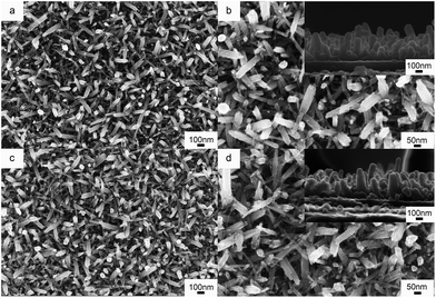
3.1.1 Effect of substrate pretreatment on microstructure and morphology of as-prepared WNRAs film. It is known that the structure and morphology of the WO3 thin film played important roles in determining its EC properties. In our previous works, the effect of the WO3 seed layer on the formation of the WNRAs was discussed in detail.25 With the existence of the seed layer on FTO substrate, the uniform and well aligned WNRAs film was obtained compared with the film grown on bare FTO substrate. However, there was a problem that the film was easy to fall off due to its poor cohesiveness between the seed layer and FTO substrate, leading to not good EC properties. Therefore, in this paper, we substituted the WO3 seed layer with the TiO2 seed layer to improve the contact between the film and FTO substrate, and further to investigate the new seed layer's effect on the morphology and EC properties of synthesized WNRAs film. Fig. 1 showed the SEM images of the WNRAs in AW and ATi700, respectively. Vertical growth of the WO3 nanorods in AW and ATi700 can both be seen from Fig. 1, and the shapes of the nanorods were almost the same. This suggests that a TiO2 seed layer could also provide many active positions for the nucleation of the WO3 particles and further lead to the formation of the WNRAs. The feature parameters of the WNRAs films in AW and ATi700 were summarized in Table 1. Under the same hydrothermal conditions, the nanorods in ATi700 were longer (330 nm) in axial direction and smaller (55.2 nm) in radial direction compared to those in AW samples. In addition, smaller grain size of TiO2 seed (35.0 nm) meant relatively more active positions for the nucleation of WO3 nanoparticles, which led to larger number density in ATi700 (1.0 × 10¹⁰ rods cm−2).
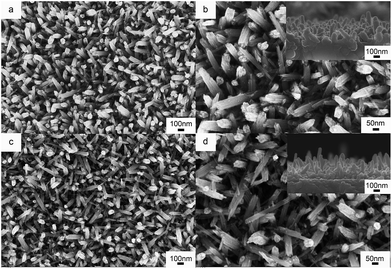 |
| | Fig. 1 SEM images of WNRAs: (a and b) AW with low magnification and high magnification; (c and d) ATi700 with low magnification and high magnification. Insets in (b and d) cross-section view of SEM images of AW and ATi700. | |
Table 1 Morphology feature parameters of WNRAs in AW and ATi700
| Sample |
Average diameter (nm) |
Average length (nm) |
Density (rods cm−2) |
Grain size of seed layer (nm) |
| AW |
57.9 |
230 |
6.9 × 10⁹ |
37.5 |
| ATi700 |
55.2 |
330 |
1.0 × 10¹⁰ |
35.0 |
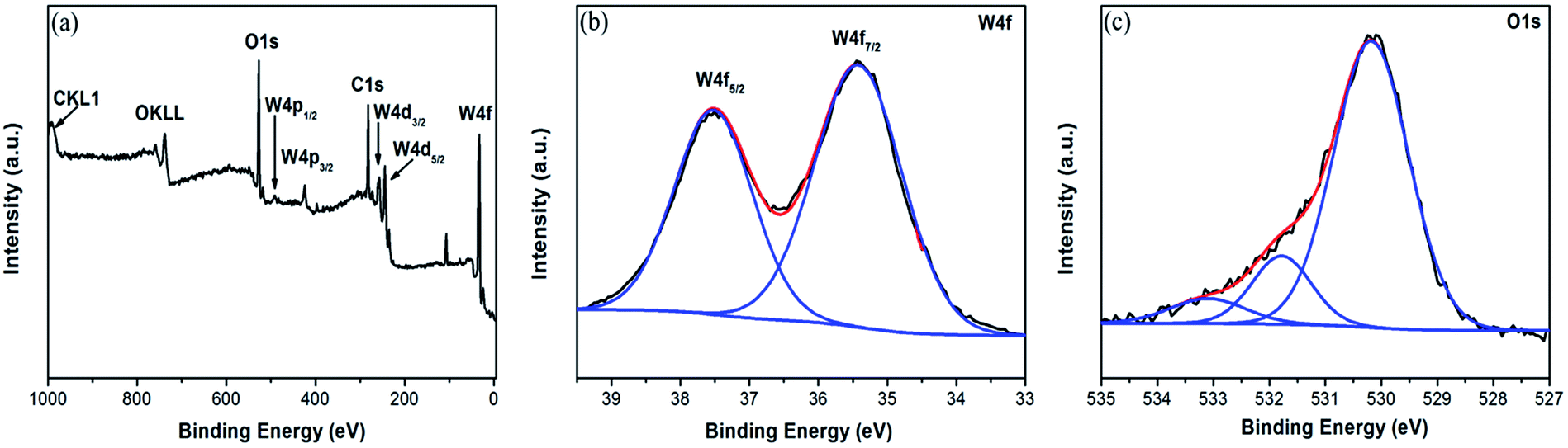
Fig. 2 gave the XPS spectra of the as-prepared ATi700. From the full spectrum, tungsten and oxide peaks could be identified obviously. The W4f core level spectrum of the ATi700 (Fig. 2(b)) exhibited well-resolved spin–orbit split doublet peaks corresponding to the W4f5/2 and W4f7/2, at 37.5 eV and 35.4 eV, respectively. This suggests that the film at bleaching state contained only W6+, which corresponded well to the result of the XRD in the ESI (Fig. S1†). Fig. 2(c) displayed the O1s core level spectrum which exhibited broad peak with high binding energy sides assigning several kinds of oxygen species. The O1s core level can be fit to yield three Gaussian curves, at binding energy 530.2, 531.8 and 533.1 eV, respectively. The component at binding energy 530.2 eV was assigned to oxygen atom (O2−) in the WO3 lattice that formed a strong bond in the manner W![[double bond, length as m-dash]](https://www.rsc.org/images/entities/char_e001.gif) O. The second peak at 531.8 eV was assigned to a small mount hydroxyl group (OH−) on the WO3 surface. The third components at binding energy 533.1 eV may be the oxygen from the atmospheric water molecule absorbed on the sample surface.26
O. The second peak at 531.8 eV was assigned to a small mount hydroxyl group (OH−) on the WO3 surface. The third components at binding energy 533.1 eV may be the oxygen from the atmospheric water molecule absorbed on the sample surface.26
 |
| | Fig. 2 XPS spectra of as-prepared ATi700 (a) full spectrum, (b) W4f and (c) O1s. | |
More detailed morphological and structural features of ATi700 and AW were studied by TEM and HRTEM as shown in Fig. 3. Single-crystalline nanorods with varying diameters were illustrated in Fig. 3(a) and (c). From Fig. 3(b), it can be seen that the spacing of the lattice fringes was about 0.39 nm, which was well indexed to the (001) plane of the hexagonal structure WO3, indicating that the WO3 nanorod growing along [001] direction. This result agreed well with XRD pattern in Fig. S1.† In addition, it is also found that the lattice fringes of the nanorod were not distinct, suggesting that the crystallinity of the prepared nanorods on TiO2 seed layer was not so high, which was similar to those in AW (Fig. 3(d)).10 This meant that the substitution of the TiO2 seed layer could not change the crystallinity of the synthesized WO3 nanorods significantly.
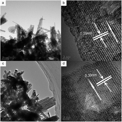 |
| | Fig. 3 (a) TEM and (b) HRTEM images of ATi700, (c) TEM and (d) HRTEM images of AW. | |
The formation mechanism of the as-prepared AW was investigated in our previous work.27 Like the WO3 seed layer, the TiO2 seed layer could provide more active positions than bare FTO substrate for further formation of nanorods, and the seed layers with relatively high crystallinity also helped the well orientation of the nanorods to form array structure. The method of adding addictives into the precursor to control the final morphology during the hydrothermal process is now common. With the different kinds of ions (cations, anions) added, the morphology of the WO3 films was diverse. Zhang et al.8 used (NH4)2SO4 as the addictive and thought that sulfate ions preferentially absorbed on the faces parallel to the c-axis of WO3 nanocrystal, thus 1D single crystal nanowires were formed. In this paper, rubidium sulfate was used as the addictive and the as-prepared nanorod arrays showed a lower aspect ratio. So, we speculated that the cations could also affect the shaping of the 1D nanostructures. In this case, the Rb+ ions were supposed to might preferentially inhibit the growth of the rods on the axial direction, resulting in the low aspect ratio of the nanorods. When the amount of the rubidium sulfate was reduced, the nanorods with smaller diameters were obtained, which agreed well with our assumption.
More importantly, it should be noted that the as-prepared WNRAs film grown on the FTO substrates pre-coated with TiO2 seed layer showed higher structure stability compared with that on WO3 seed layer, suggesting that the TiO2 seed layer has better adhesion ability to the FTO substrates. The main reasons might be ascribed to the follows: firstly, the fluoride doped SnO2 (the conductive side of FTO substrate) has the same tetragonal rutile structure as rutile structure TiO2 crystal seeds after annealing at 700 °C, so, the lattice mismatch between FTO substrate and TiO2 was only 2%,28 much lower than that between FTO substrate and WO3 seeds layer (about 22%). This small lattice mismatch may promote the epitaxial nucleation of the TiO2 nanoparticles of the seed layer, ensuring the seed layer had good crystallinity and good contact with the FTO substrate. Secondly, the extra H2O2 contained in preparing of WO3 colloid solution would produce O2 during the annealing process, so, the escape of O2 between the FTO substrate and the colloid solution may further impact the contact of the substrate and the seed layer, resulting in the WO3 seed layer easier falling off the substrate.
3.1.2 Effect of substrate pretreatment on EC properties of as-prepared WNRAs films. Generally, the characteristic parameters of WO3 for EC properties are the cycling stability, optical modulation, responding times, and coloration efficiency. And the cycling stability is considered as one of the most important factors for EC properties. Generally, the cyclic voltammograms (CVs) is used to elucidate the cycling stability of WO3. Fig. 4 showed the CV curves of the ATi700 between −1.0 and 1.0 V at a scan rate of 50 mV s−1 for 1st, 500th and 1000th cycles. As can be seen from the CVs, these WO3 films gave a pair of redox peaks which could be ascribed to the intercalation/deintercalation of both Li+ ions and electrons into/out of the WO3 crystal lattice, represented as the following equation:1| | |
WO3 (transparent) + xe− + xLi+ ↔ LixWO3 (blue)
| (1) |
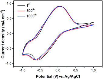 |
| | Fig. 4 Cyclic voltammetry curves of ATi700 at 1st, 500th and 1000th cycles in 1 mol L−1 LiClO4/PC at the scanning speed of 50 mV s−1 between −1.0 V and +1.0 V. | |
It should be noted that no significant change in the shape of CVs appeared during the periods of 1000 cycles, suggesting good cycling stability of the as-prepared ATi700. In addition, the double ions intercalation/deintercalation capacities of the WNRAs film could be calculated by integrating the cathodic/anodic current density, which was equal to the amount of Li+ ions and electrons intercalated into/deintercalated out of the WNRAs film to form a blue LixWO3 film/transparent WO3 film. When the WNRAs film cycled for 1000th, the total cathodic and anodic charge quantities became stable and were calculated to be about 17.2 and 14.9 mC cm−2 respectively, implying there were still Li+ ions remaining in the ATi700 at the bleaching state. In addition, it could be found from the SEM images (Fig. S2†) that the nanorod arrays was unchanged after the CV test, indicating the good structure and cycling stability of ATi700.
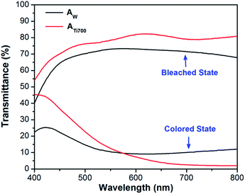
Fig. 5 illustrated the visible transmittance spectra of AW and ATi700 in colored and bleached states at −3.0 V and +3.0 V (vs. Ag/AgCl) for 100 s, respectively. Comparing with the sample AW, the ATi700 presented larger transmittance at bleached state (81.0%) and lower transmittance at colored state (3.5%) when the wavelength was longer than 600 nm, resulting in a larger optical modulation of 77.5% at the wavelength of 660 nm, which was also larger than those in the former reports.29,30 The obtained results were in accordance with that of Reyes-Gil et al.31 This phenomenon may be ascribed to the following reasons: the structures of the samples AW and ATi700 were composed of two parts including the different seed layers of WO3/TiO2 and the similar WNRAs grown on the seed layers. It should be noticed that TiO2 is also a kind of EC materials. The transmittance modulation of the as-annealed TiO2 and WO3 seed layers were also measured under the same experimental conditions, respectively as shown in Fig. S3.† It can be found that the transmittance modulation of the TiO2 seed layer was very small (about 3%) at the wavelength of 660 nm while that of WO3 seed layer was 24%. Considering the similar WNRAs grown on the two seed layers, the color's change of ATi700 was mostly attributed to the properties of the WNRAs rather than TiO2 seed layer, while that of AW was ascribed to the properties of the WNRAs along with WO3 seed layer, which would lead to lower modulation of AW than ATi700.
 |
| | Fig. 5 The visible transmittance spectra of ATi700 (red line) and AW (black line) at colored and bleached states measured at −3.0 V and +3.0 V for 100 s, respectively. | |
Fig. 6 gave the digital photographs of WNRAs film in colored and bleached states. It can be clearly seen that the WNRAs film showed a uniform deep blue color by applying a potential of −3.0 V, while the color of the film was quickly bleached to colorless by applying a potential of +3.0 V, revealing good color reversibility of the film.
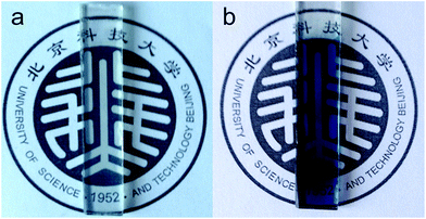 |
| | Fig. 6 Digital pictures of ATi700 at (a) bleached state (measured at +3.0 V for 100 s) and (b) colored state (measured at −3.0 V for 100 s). | |
Fig. 7(a) presented the in situ coloring/bleaching transmittance response of AW and ATi700 tested at 660 nm. It can be seen that ATi700 showed a good reversibility and a bit decrease of the modulation at bleached state after the first recycle. It is speculated that there were still Li+ ions stuck in the nanorods in ATi700, which was corresponding to the result of the CV test. The switching time was defined as the time required for 90% change in the full transmittance modulation at a certain wavelength (660 nm in this case). As indicated in Fig. 7(b), the switching time of ATi700 for coloring and bleaching were 10 s and 28 s, while AW exhibited 26 s for coloring and 24 s for bleaching, respectively, which were not so fast when compared with some former reports,9,32 due to the larger size of the WO3 nanorods. The ATi700 showed a much shorter response time than AW, which may be explained as follows: the larger diameters (57.9 nm) of the nanorods in AW made the diffusion lengths for Li+ in each single nanorod longer than that (55.2 nm) in ATi700. With more ions intercalated into the larger nanorods, they would cause a stronger electronic field to resist the following ions' intercalation. In addition, the high crystallographic TiO2 seed layer and its good contact with the substrate facilitated the fast transfer of electrons from the substrate to the nanorods, resulting in the faster coloring response of ATi700. Furthermore, there might be some Li+ ions to intercalate the WO3 seed layer in AW, delaying the coloring time.
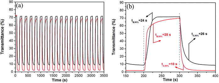 |
| | Fig. 7 The switching response characteristics: (a) optical response of ATi700 (red solid line) and AW (black solid line) through chronoamperometry method at +3.0 V and −3.0 V application for 100 s per step at 660 nm; (b) the switching time of ATi700 (red solid line) and AW (black solid line) measured at ±3.0 V for 100 s, respectively. | |
In addition, it should be noticed that the bleaching time of ATi700 was longer than its coloring time, which may be explained by the EC mechanism of the WNRAs as illustrated in Fig. 8. When negative voltage was applied, Li+ ions diffused from the electrolyte to the surface of the nanorods. Due to the special lattice structure of h-WO3, three possible channels33 (trigonal cavity, hexagonal window and four-coordinated square window) facilitated the ions' transfer and accommodation. For the faster transfer in the substrate and the nanorods, the electrons combined the Li+ ions to form the LixWO3 when the ions were just injected into the lattices. When the following Li+ ions intercalated into the nanorods, they combined the already existed electrons very quickly, leading to the rapid decrease of the transmittance. The Li+ ions would soon reach saturation with more Li+ ions in the WO3 lattices and began to resist the subsequent ions diffusion, so the coloring process slowed down. On the contrary, when the positive voltage was applied, the electrons and Li+ ions were driven to deintercalate out of the lattices, back to the substrate and electrolyte. The Li+ ions intercalated near the surface were easy to transfer into the electrolyte, resulting in a fast rise in transmittance of the bleaching process. The electrostatic interaction between the electrons/Li+ ions and the Li+ ions in the electrolyte limited the deintercalation of the inner Li+ ions, leading to a longer bleaching time.
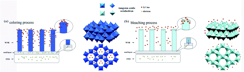 |
| | Fig. 8 The EC mechanism of the WNRAs: the interface reaction process of Li+ ions and electrons between WO3 and the electrolyte as well as the diffusion process of Li+ ions and electrons in the WO3 crystal lattice of (a) coloring process and (b) bleaching process. | |
Another important characteristic parameter of the EC properties is coloration efficiency (CE), which is defined as the change in optical density (OD) per unit of charge inserted into (or extracted from) the EC film. It can be calculated from the following equations:34,35
where
Tc and
Tb denote the transmittance of the film at its colored and bleached state, respectively, and the
Q is the corresponding injected (or ejected) charge density per unit area.
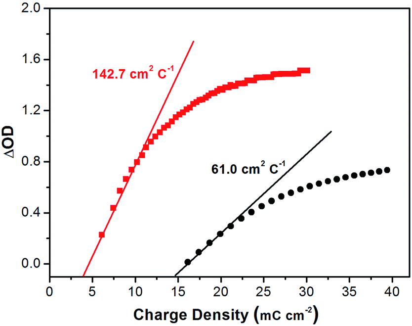
Fig. 9 illustrated the plots of the optical density (ΔOD) varying with the charge density (
Q) of A
W and A
Ti700. The CE value was calculated as the slope of the line fitted to the linear region of the curve. A large CE value meant the EC film could exhibit a large optical density modulation with a small charge inserted (or extracted). The CE value of A
Ti700 could be up to 142.7 cm
2 C
−1, while that of A
W was 61.0 cm
2 C
−1, which could be compared with that in the former reports.
7,36 Combining the results shown in Fig. S4, S6
† and
7, it can be concluded that, for A
Ti700, a major modulation of transmittance could be completed in a shorter time after voltage switching. However, as for A
W, it took longer time and more charge to accomplish the saturation of OD. So, when applied to
eqn (3), the A
Ti700 showed a lager ΔOD value than A
W with smaller charge density. The relatively larger size of the nanorods in A
Ti700 was benefit for the electrolyte's immersing in the film, resulting in more Li
+ ions having better contact with the nanorods to make the full use of the surface area. Meanwhile, the TiO
2 seed layer also contributed to the larger CE value of A
Ti700. The excellent stability of the TiO
2 itself and the good contact between the seed layer and FTO substrate/nanorods would make the fast and uniform diffusion of the electrons inserting into or extracting out of the nanorods. And the conduction band of WO
3 was higher than that of TiO
2,
37 leading to the electrons easier to transfer from TiO
2 to WO
3 for the driving force caused by the energy level difference. Thus, a large optical density modulation could be obtained with a small charge density.
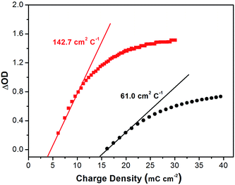 |
| | Fig. 9 The variation of the in situ optical density (ΔOD) vs. the charge density for ATi700 (red square) and AW (black dot) measured at 660 nm. | |
3.2 The effect of annealing temperature of the TiO2 seed layers on microstructure and EC properties of as-prepared WNRAs films
According to our previous work,15 with increasing the annealing temperature of seed layer, the grain size and the crystallinity of the seeds increased, which would affect the morphology and size of the nanorod arrays grown on it. Fig. 10 showed the SEM images of the ATi550 and ATi650, and the corresponding morphology feature parameters were summarized in Table 2. It can be seen that both ATi650 and ATi550 had vertical grown orientation and similar shapes of rods. With increasing of the annealing temperature of the seed layers, the average diameter and length of as-prepared WNRAs increased from 48.2 to 55.2 nm, and 240 to 330 nm, respectively, which was mainly ascribed to the increasing grain size of the TiO2 seeds from 15.0 to 35.0 nm (Fig. S5(a)–(c)†).
 |
| | Fig. 10 SEM images of (a and b) ATi550 with low magnification and high magnification; (c and d) ATi650 with low magnification and high magnification. Insets in (b and d) cross-sectional view of SEM images of ATi550 and ATi650. | |
Table 2 Morphology feature parameters of WNRAs in ATi550, ATi650 and ATi700
| Sample |
Average diameter (nm) |
Average length (nm) |
Grain size of seed layer (nm) |
| ATi550 |
48.2 |
240 |
15.0 |
| ATi650 |
53.6 |
275 |
25.0 |
| ATi700 |
55.2 |
330 |
35.0 |
Fig. 11 illustrated the EC performances of ATi550, ATi650 and ATi700. Considering the same TiO2 seed layer pre-coated on FTO substrates, the morphology variation of the WNRAs might be the main reason for the different EC properties of ATi550, ATi650 and ATi700. As shown in Fig. 11(a), ATi650 exhibited a similar optical modulation (77.4%) with ATi700 (77.5%), which was larger than ATi550 (72.7%) and AW (62.8%) at the wavelength of 660 nm, further confirming the effect of the TiO2 seed layer on improving the EC performance of WNRAs. Compared with the ATi700, both the WNRAs in ATi550 and ATi650 showed good reversibility, stability and faster response time as illustrated in Fig. 11(b) and (c). Specifically, with the annealing temperature increasing from 550 to 700 °C, the bleaching time of the WNRAs increased from 2.4 to 6.2 and 28 s while the coloring time changed a little (7.3, 12, 10 s), which may be mainly due to the increasing lengths and diameters of the WNRAs in ATi550 to ATi700. It can be also seen in Fig. 11(d) that the ΔOD values changed little in ATi550 and ATi650 with the charge density lower than 10 mC cm−2, meanwhile, ATi650 had a larger optical modulation (77.4%) and a lower Tc (transmittance at colored state, 9.3%), so, when applied to eqn (3), with smaller values of Tc as the denominators, a series of higher ΔOD values could be gained. Combing the higher ΔOD values and nearly the same charge density values, a higher CE value was obtained in ATi650 (89.0 cm2 C−1) than ATi550 (74.5 cm2 C−1). Although ATi700 showed a little larger charge density values corresponding to the ordinal ΔOD values, the larger optical modulation and rather small Tc (2.0%) enabled it to obtain a higher CE value (142.7 cm2 C−1).
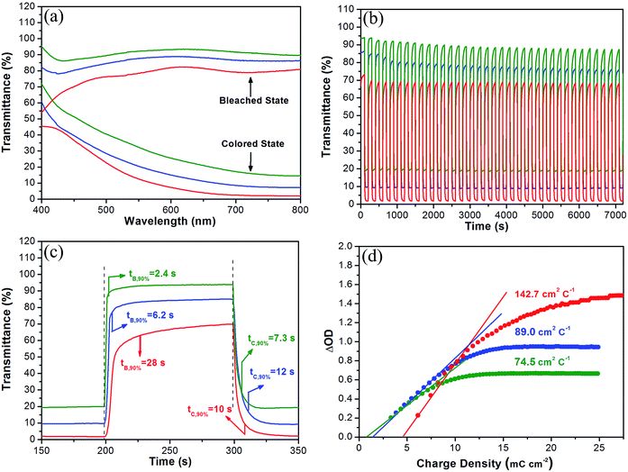 |
| | Fig. 11 EC performances of ATi550 (green), ATi650 (blue) and ATi700 (red): (a) the visible transmittance spectra at colored and bleached states measured at ±3.0 V for 100 s, respectively; (b and c) switching time characteristics between colored and bleached states measured at ±3.0 V with a wavelength of 660 nm; (d) coloration efficiencies measured at 660 nm. | |
4 Conclusions
In summary, WNRAs was synthesized on FTO substrate pre-coated with TiO2 seed layer by using a hydrothermal method. The introduction of the TiO2 seed layer did not change the morphology of the as-prepared WNRAs greatly when compared with those grown on WO3 seed layer. The TiO2 seed layer had great effect on the EC performance of the WNRAs. Due to the excellent adhesion and contact between the TiO2 seed layer and the FTO substrate, the ATi700 showed larger modulation of transmittance (77.5%) and higher CE value (142.7 cm2 C−1). Moreover, with increasing the annealing temperature of the TiO2 seed layers, all the WNRAs grown on them exhibited larger modulation of transmittance, faster response time and higher CE value. The small changes of the EC properties maybe mainly ascribed to their corresponding different thickness and diameter of the formed WNRAs. The high CE value, large modulation of transmittance and good stability make the WNRAs thin film promising to apply in practical EC devices.
Acknowledgements
The work was financially supported by the National Science Foundation of China (No. 51272025 and 51572020), the National Basic Research Program of China (No. 2014CB643401, 2013AA032003), and China Postdoctoral Science Foundation (No. 2015M581581).
References
- B. W. Faughnan, R. S. Crandall and P. M. Heyman, RCA Rev., 1975, 36, 177–197 CAS.
- C. Santato, M. Odziemkowski, M. Ulmann and J. Augustynski, J. Am. Chem. Soc., 2001, 123, 10639–10649 CrossRef CAS.
- M. Feng, A. L. Pan, H. R. Zhang, Z. A. Li, F. Liu, H. W. Liu, D. X. Shi, B. S. Zou and H. J. Gao, Appl. Phys. Lett., 2005, 86, 141901 CrossRef.
- S. Das and W. M. A. Wan Daud, RSC Adv., 2014, 4, 20856–20893 RSC.
- M. Penza, G. Cassano and F. Tortorella, Sens. Actuators, B, 2001, 81, 115–121 CrossRef CAS.
- K.-I. Choi, S.-J. Hwang, Z. Dai, Y. Chan Kang and J.-H. Lee, RSC Adv., 2014, 4, 53130–53136 RSC.
- S. Gubbala, J. Thangala and M. K. Sunkara, Sol. Energy Mater. Sol. Cells, 2007, 91, 813–820 CrossRef CAS.
- J. Zhang, J. P. Tu, X. H. Xia, X. L. Wang and C. D. Gu, J. Mater. Chem., 2011, 21, 5492–5498 RSC.
- D. Y. Ma, G. Y. Shi, H. Z. Wang, Q. H. Zhang and Y. G. Li, J. Mater. Chem. A, 2013, 1, 684–691 CAS.
- F. Zheng, W. K. Man, M. Guo, M. Zhang and Q. Zhen, CrystEngComm, 2015, 17, 5440–5450 RSC.
- G. F. Cai, J. P. Tu, D. Zhou, X. L. Wang and C. D. Gu, Sol. Energy Mater. Sol. Cells, 2014, 124, 103–110 CrossRef CAS.
- J. H. Qiu, M. Guo, Y. J. Feng and X. D. Wang, Electrochim. Acta, 2011, 56, 5776–5782 CrossRef CAS.
- T. Ma, M. Guo, M. Zhang and X. D. Wang, J. Nanosci. Nanotechnol., 2009, 9, 5920–5926 CrossRef CAS.
- Y. X. Li, M. Guo, M. Zhang and X. D. Wang, Mater. Res. Bull., 2009, 44, 1232–1237 CrossRef CAS.
- M. J. Gao, Y. X. Li, M. Guo, M. Zhang and X. D. Wang, J. Mater. Sci. Technol., 2012, 28, 577–586 CAS.
- C. Y. Ng, K. A. Razak and Z. Lockman, J. Alloys Compd., 2014, 588, 585–591 CrossRef CAS.
- C. P. Li, F. Lin, R. M. Richards, C. Engtrakul, R. C. Tenent and C. A. Wolden, Sol. Energy Mater. Sol. Cells, 2014, 121, 163–170 CrossRef CAS.
- Y. Yamada, K. Tabata and T. Yashima, Sol. Energy Mater. Sol. Cells, 2007, 91, 29–37 CrossRef CAS.
- T. Pauporté, J. Electrochem. Soc., 2002, 149, C539–C545 CrossRef.
- J. Thangala, S. Vaddiraju, S. Malhotra, V. Chakrapani and M. K. Sunkara, Thin Solid Films, 2009, 517, 3600–3605 CrossRef CAS.
- E. Khoo, P. S. Lee and J. Ma, J. Eur. Ceram. Soc., 2010, 30, 1139–1144 CrossRef CAS.
- J. M. Wang, E. Khoo, P. S. Lee and J. Ma, J. Phys. Chem. C, 2008, 112, 14306–14312 CAS.
- D. Y. Ma, H. Z. Wang, Q. H. Zhang and Y. G. Li, J. Mater. Chem., 2012, 22, 16633–16639 RSC.
- S. Adhikari and D. Sarkar, RSC Adv., 2014, 4, 20145–20153 RSC.
- F. Zheng, H. Lu, M. Guo and M. Zhang, CrystEngComm, 2013, 15, 5828–5837 RSC.
- V. V. Kondalkar, S. S. Mali, R. R. Kharade, R. M. Mane, P. S. Patil, C. K. Hong, J. H. Kim, S. Choudhury and P. N. Bhosale, RSC Adv., 2015, 5, 26923–26931 RSC.
- F. Zheng, M. Guo and M. Zhang, CrystEngComm, 2013, 15, 277–284 RSC.
- B. Liu and E. S. Aydil, J. Am. Chem. Soc., 2009, 131, 3985–3990 CrossRef CAS PubMed.
- G. Cai, X. Wang, D. Zhou, J. Zhang, Q. Xiong, C. Gu and J. Tu, RSC Adv., 2013, 3, 6896–6905 RSC.
- G. Cai, J. Tu, D. Zhou, L. Li, J. Zhang, X. Wang and C. Gu, CrystEngComm, 2014, 16, 6866–6872 RSC.
- K. R. Reyes-Gil, Z. D. Stephens, V. Stavila and D. B. Robinson, ACS Appl. Mater. Interfaces, 2015, 7, 2202–2213 CAS.
- D. Zhou, D. Xie, F. Shi, D. H. Wang, X. Ge, X. H. Xia, X. L. Wang, C. D. Gu and J. P. Tu, J. Colloid Interface Sci., 2015, 460, 200–208 CrossRef CAS PubMed.
- S. Balaji, Y. Djaoued, A. S. Albert, R. Z. Ferguson and R. Bruning, Chem. Mater., 2009, 21, 1381–1389 CrossRef CAS.
- D. Ma, G. Shi, H. Wang, Q. Zhang and Y. Li, J. Mater. Chem. A, 2014, 2, 13541–13549 CAS.
- Y. C. Her and C. C. Chang, CrystEngComm, 2014, 16, 5379–5386 RSC.
- L. Liang, J. Zhang, Y. Zhou, J. Xie, X. Zhang, M. Guan, B. Pan and Y. Xie, Sci. Rep., 2013, 3, 1936 Search PubMed.
- M. Miyauchi, A. Nakajima, T. Watanabe and K. Hashimoto, Chem. Mater., 2002, 14, 4714–4720 CrossRef CAS.
Footnote |
| † Electronic supplementary information (ESI) available: X-ray diffraction pattern, visible spectra of as-prepared seed layers, plots of current density vs. time of the samples, EIS and so on. See DOI: 10.1039/c5ra20970f |
|
| This journal is © The Royal Society of Chemistry 2015 |
Click here to see how this site uses Cookies. View our privacy policy here.