Yumei Wangab,
Nishuang Liua,
Ying Chena,
Congxing Yanga,
Weijie Liua,
Jun Sua,
Luying Lia and
Yihua Gao*a
aCenter for Nanoscale Characterization & Devices (CNCD), Wuhan National Laboratory for Optoelectronics (WNLO)-School of Physics, Huazhong University of Science and Technology (HUST), Luoyu Road 1037, Wuhan 430074, China. E-mail: gaoyihua@hust.edu.cn
bZhoukou Normal University, Wenchang Road, Zhoukou 466001, China
First published on 3rd December 2015
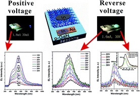
Incorporation of Cu atoms in ZnO can arouse Cu-related defect, which will influence electroluminescence (EL) light of light emitting diode (LED) based on ZnO:Cu/p-GaN heterojunction. ZnO:Cu nanobushes were grown on p-GaN film by simple chemical vapour deposition (CVD) method. Ultraviolet (UV) photoluminescence (PL) peak of ZnO:Cu had a redshift compared with that of pure ZnO, and low temperature (5 K) PL spectrum exhibited a structured green emission, indicating the substitutional incorporation of Cu atoms in ZnO crystal lattice. The LED based on ZnO:Cu/p-GaN heterojunction emitted blue-greenish EL light at p-GaN site at the positive bias voltage, and green EL peak gradually overtook the blue EL peak with the increase of positive bias voltage. At reverse bias voltage, this LED not only exhibited yellow-green EL light at ZnO:Cu site, but also emitted from orange to yellow EL light at p-GaN site with the increase of reverse bias voltage. The origins of EL light at positive and reverse bias voltage were explained using PL spectra and energy band diagram of ZnO:Cu/p-GaN structure.
The LED based on pure ZnO/p-GaN heterojunction usually emits UV or/and blue light.2,5 Doping with selective elements is a common method, which can manipulate the defects in ZnO to adjust the electronic and optical properties of ZnO-based LED. Actually, the band gap of ZnO can be tuned by doping Ga in ZnO, so the LED based on GaxZn1−xO/p-GaN can emit from UV (382 nm) to visible (478 nm) light by changing the content of doped Ga.6 Transition metal Cu is adjacent with Zn element in the periodic table of elements and has the similar ionic radii sizes and configurations of outer electron shells with Zn. Cu is a prominent luminescence activator in II–VI compounds.7 So Cu is one of the preferable dopant to tune electronic and optical property of ZnO. The incorporation of Cu atoms in ZnO can narrow the bandgap of ZnO, and electroluminescence (EL) emission of Cu-doped ZnO/p-GaN LEDs shifted from UV to violet-blue spectral region compared to pure ZnO/p-GaN LEDs.8 In addition, Cu dopant arouses deep level defect state in the band gap of ZnO, which is considered to be responsible for green photoluminescence (PL) emission in ZnO.9–11 Dingle9 suggested that deep level defect in Cu doped ZnO is due to the charge transfer between Cu2+ ions and adjacent oxygen atoms (hole transfers from d shell to sp3 orbitals). Graces10 claimed that Cu in ZnO may exist in Cu+ or Cu2+ state, and aroused not only unstructured green PL emission by donor–acceptor pair recombination involving the Cu+ acceptors, but also structured green PL emission related to Cu2+ ions. Cu dopant in ZnO will also influence EL light of ZnO-based LED. LEDs based on Cu doped ZnO/p-GaN heterojunction were fabricated using different methods such as thermal diffusion,8 filtered cathodic vacuum arc,12 electrodeposition,13–15 hydrothermal method.16,17 The formation energy of the group-IB element Cu in ZnO is low under the O-rich condition.18,19 Therefore, ZnO:Cu nanobushes were grown on p-GaN film by simple chemical vapour deposition (CVD) method under the O-rich condition in this study. The LED based on ZnO:Cu/p-GaN heterojunction emitted multicolour EL lights at different positive and reverse bias voltage. At the positive bias voltage, this LED emitted blue-greenish electroluminescence (EL) light at p-GaN site. At reverse bias voltage, this LED not only exhibited yellow-green EL light at ZnO:Cu site, but also emitted from orange to yellow EL light at p-GaN site with the increase of reverse bias voltage.
The PL measurements of pure ZnO and ZnO:Cu on p-GaN film, and p-GaN film at RT were measured, respectively. The PL spectra of ZnO:Cu/p-GaN structure and p-GaN film were shown in Fig. 2a. The band edge emission of about 365 nm in the PL spectrum of p-GaN film is attributed to the exciton recombination, and the blue emission peak ascribe to the transition between the conduction band and deep Mg-dopant induced acceptor levels22 in p-GaN. And a near-band-edge emission of 383 nm and a defect related visible band emission in region from green to red can be observed in the spectrum of ZnO:Cu/p-GaN structure. In addition, the normalized PL spectra of the pure ZnO and ZnO:Cu at higher energy are presented in the inset of Fig. 2a. The UV peak of ZnO:Cu (383 nm, 3.237 eV) had a red-shift of ∼52 meV compared with that of pure ZnO (377 nm, 3.289 eV). This red-shift phenomenon of UV PL peak was attributed to the coupling between the band electrons and the localized Cu2+ impurity spin,23 which reduced bandgap of ZnO. And the red-shift also indicated that Cu partially substituted for Zn atoms in the ZnO crystal lattice. On the other hand, the visible emissions from green to red in the ZnO:Cu/p-GaN structure is the result that Cu doping in ZnO aroused much more intrinsic and extrinsic defects.8 Visible PL light are related to deep level energy emission, which probably originated from the extrinsic defect from Cu dopant and the intrinsic defects of Zni, VO, zinc vacancy (VZn), and oxygen interstitial (Oi).9–11,24,25 According to the prior literatures,11,24,25 the Cu dopants at Zn sites can result in the green PL emission,11 and the Oi defect can lead to the orange-yellow broad PL emission.24 In addition, the red PL emission can be ascribed to the band transition from the VO energy level to the top of the valence band in ZnO:Cu.25 Moreover, structured green emission in low temperature PL spectrum is typical characteristic in ZnO containing Cu.9–11 So PL spectrum of ZnO:Cu in green region was also measured in low temperature (5 K), as shown in Fig. 2b. The structured green PL emission with an LO-phonon energy interval of ∼72 meV for ZnO was observed, which can be attributed to a localized excitation of a Cu2+ ion at zinc site.26 The occurrence of structured green PL emission further verified the substitutional Cu ion at zinc site in ZnO.
A schematic diagram of the ZnO:Cu/p-GaN LED device is shown in the upper inset of Fig. 2c. Au film of 10 nm thick was thermally evaporated on p-GaN part through mask. The Au layer was contacted with metal indium (In) in order to form ohmic contact with the p-GaN film. Metal In was directly contacted with ZnO:Cu. From the linear I–V Curves in the lower inset of Fig. 2c, it is deduced that ohmic contacts on each part were achieved. Fig. 2c shows I–V characteristics of the fabricated Cu:ZnO/p-GaN structure measured at RT with p-GaN as the positive pole through a two-probe station. The non-linear I–V curve exhibits rectifying diode-like behaviour, which bespeaks possibility of light emission.
The EL spectra from ZnO:Cu/p-GaN LED device were measured at various positive and reverse bias voltages with a direct current source meter at RT. A high-sensitivity fibre optic spectrometer collected EL light of this LED. The photos of EL light at positive bias voltages from 20 V to 30 V are shown in Fig. 3a. The blue-greenish EL light came from p-GaN site (right side) and could be observed with the naked eye in a dark environment. However, no EL emission light was detected at ZnO:Cu site (left side). The EL spectra in p-GaN region at different positive bias voltages are shown in Fig. 3b. Fig. 3c shows EL spectrum at positive bias voltage of 24 V which was Gaussian fitted with blue peak at 414 nm and green peak at 556 nm. From Fig. 3b, we observed that the intensity of main emission in EL spectra increased and intensity of green EL gradually overtook blue EL with the elevation of positive bias voltage. No obvious shift of peak location was observed in EL spectra.
When reverse bias voltages were applied on this LED device, the ZnO:Cu/p-GaN region emitted yellow-green light. Meanwhile, p-GaN site emitted from orange to yellow light with the elevation of reverse bias voltage. This phenomenon can be observed from the photos of EL light at reverse bias voltages from 20 V to 30 V in Fig. 4a. The corresponding EL spectra were shown in Fig. 4b and c, respectively. Obviously, the light emission behaviours at reverse bias voltages are different from that at forward biased voltages. The EL light from p-GaN site changed from orange to yellow and blue-shifted from 651.6 nm to 613.5 nm with the elevation of reverse bias voltage. The yellow-green EL peak from ZnO:Cu site at positive bias voltage of 30 V was divided into two peaks. One is corresponding to the EL fitted peak from p-GaN site at the same reverse bias voltage, and the other divided peak will be centred at around 550 nm. The same fitting procedures of EL curves at reverse bias voltage from 22 V to 30 V were also performed. It is found that the divided peak at around 550 nm always remains constant.
In order to account for the origin of EL peak at positive and reverse bias voltages, energy band diagram of ZnO:Cu/p-GaN heterojunction is illustrated in Fig. 5a, which exhibits type II band alignment with an interface configuration-dependent valence band offset having an average value of 1.6 eV.27 Energy band diagram of ZnO:Cu/p-GaN heterojunction at positive bias voltages is described in Fig. 5b. Electrons from the conduction band of ZnO:Cu arrived at the ZnO:Cu/GaN interface and were captured by the deep-level states near the interface such as VO or/and Cu induced deep level,28 thus yielding green band around 556 nm. The carrier mobility of electron in the ZnO:Cu is higher than that of the p-GaN due to the difference in the effective mass and carrier scattering mechanism. Electrons could not be completely blocked in the ZnO:Cu region and will pass through the interface. Some of the electrons in ZnO:Cu will inject into the p-GaN site to recombine with deep Mg acceptor level defects in p-GaN which leads to blue emission at p-GaN site,29 corresponding with the blue peak in PL spectrum of p-GaN. When the applied positive voltage increased, more electrons arrived at ZnO/GaN interface and recombination at the interface increased more rapidly, overtook the recombination between electron that passed through the interface and deep Mg acceptor level defects in p-GaN. It is consistent with the EL spectra in p-GaN region at different positive bias voltages. Fig. 5c described energy band diagram of ZnO:Cu/p-GaN heterojunction at reverse bias voltages. When reverse bias voltage was applied on this heterojunction, the thickness of tunnelling barrier became very thin either by lowering the ZnO conduction band or by raising the valence band of GaN as a result of large band offset. The occupied states of the valence band of p-GaN would be higher than the unoccupied states of the conduction band of ZnO:Cu, which will results in the movement of electrons toward lower energy than the recombination with acceptors in the valence band of GaN. Thus blue light related with the transition from the conductive band to deep Mg acceptor level defects in p-GaN will not appear. The recombination related with electron that tunnelled from p-GaN to ZnO:Cu will occur at the ZnO:Cu site, and stable green emission light of 550 nm resulting from substitutional Cu+ and Cu2+ at zinc site10 would be emitted. It is also consistent with the PL green peak of ZnO:Cu/p-GaN structure. For EL light from p-GaN site, blue-shifted from 651.6 nm to 613.5 nm with the elevation of reverse bias voltage, which was also contained in yellow-green EL light at ZnO:Cu site. So it is considered as the interface recombination radiation in ZnO:Cu/p-GaN interface. Kishwar30 considered that a broad orange-red EL band centred at 650 nm is associated with the transition from the conduction band of ZnO to Oi combined with recombination from Zni to Oi in ZnO/p-GaN LED. Based on this case, the increase of the reverse bias voltage further lower the ZnO conduction band or raised the valence band of GaN, the electron which tunnelled from p-GaN to ZnO:Cu may possess higher energy,31 thus the recombination of the electrons in the conduction band of ZnO with Oi acceptor level produce photons with relatively higher energy, leading to a continuous blue shift of the EL emission peak in ZnO:Cu/p-GaN interface from orange to yellow.
![]() | ||
Fig. 5 Band diagram of the ZnO:Cu/p-GaN heterojunction (a) at zero voltage. (b) At positive bias voltage. (c) At reverse bias voltage. |
This journal is © The Royal Society of Chemistry 2015 |