Electrochemical Ostwald ripening and surface diffusion in the galvanic displacement reaction: control over particle growth

Tapas Ghosha, Prasanta Karmakarb and Biswarup Satpati*a
aSurface Physics and Material Science Division, Saha Institute of Nuclear Physics, 1/AF Bidhannagar, Kolkata-700064, India. E-mail: biswarup.satpati@saha.ac.in; Fax: +91 33 2337 4637
bVariable Energy Cyclotron Centre, 1/AF Bidhannagar, Kolkata 700064, India

Received 1st October 2015 , Accepted 19th October 2015

First published on 19th October 2015


Abstract

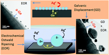
We report the role of electrochemical Ostwald ripening and the galvanic displacement reaction in uniform particle formation on ion bombarded amorphous (i.e., composed of random atomic spacings) Ge (a-Ge) surfaces compared to crystalline germanium (c-Ge). Silver growth on c-Ge and a-Ge substrates by electroless deposition has been studied by atomic force microscopy (AFM), cross-sectional transmission electron microscopy (XTEM), and energy dispersive X-ray spectroscopy (EDX). Introduction of defects can provide a control over particle growth by the galvanic displacement reaction that may offer continuous film growth up to a definite thickness. The possibility of surface diffusion and its consequences have also been discussed.


1. Introduction

Due to its technological importance, time and cost effectiveness, and exploration for atomic level deposition, electroless deposition has broadened the applicability of metal deposition techniques in many respects. The electroless processes include the autocatalytic process, the substrate catalytic process and the galvanic displacement reaction, these require no external applied voltage, which ensures immense purity in comparison with electrolytic plating. In this way, decades ago metal–metal deposition was introduced with nickel deposition on steel.1 In the autocatalytic process the prerequisites are a reducing agent, pH adjuster and other additives. Once the autocatalytic process starts, the electrons are supplied by the deposited metal ions themselves with a final charge acceptance from the reducing agent, giving rise to the feasible growth of a desired film thickness. The substrate catalytic process is accomplished on the substrate surface accompanied by a reducing agent, but the deposition is hindered once a layer is formed on the substrate. The galvanic displacement reaction surprisingly appears with no external reducing agent and fall in the electroless family.

To illustrate its mechanism, applicability and substrate dependency we restrict ourselves to discussing the galvanic displacement reaction only. The galvanic displacement reaction has been successfully implemented in micro electromechanical systems (MEMS),2 where the requisite selective deposition is provided by the displacement process. Availing the galvanic displacement technique, scanning force microscope cantilevers have been successfully coated to minimize their stress factor.3 Magnetic nanodot formation is also conceivable by this technique, which has applications in ultrahigh density ROM and RAM devices. For instance, nickel deposition at a high pH value of 8 has been attained.4–7 Turning to the structural aspects, diverse nanostructure formation by the galvanic displacement technique has also been studied. Inukshuk-like silver nanostructures made up of hexagonal building blocks have been obtained with a long period of deposition; dendritic structures have also been found to be achievable.8–16 Our surface enhanced Raman scattering (SERS) study on such silver nano-inukshuks revealed an electromagnetic field enhancement, demonstrating them to be a SERS effective substrate,17 that can eventually find use in sensing devices.

To augment understanding of the underlying mechanism in the galvanic displacement reaction, several investigations have already been performed.6–8,18–29 In assistance of this reaction, metallic films on metal and metal alloy surfaces have been deposited.18–20 The deposition of noble metals such as gold, silver, platinum and palladium has been studied on semiconducting surfaces, leading to the formation of metal semiconductor interfaces.9,17,21–24,30–34 A comparative study made by depositing Au on Ge and Si surfaces revealed the formation of bonds in the case of Au–Ge interfaces where they were absent in the case of Au–Si systems.30 Strong adhesion of Au was found on GaAs, GaP and InP surfaces when the substrates were activated in an acidified solution of palladium chloride. Faceted gold nanoparticles have been produced on InP in the presence of H2SO4.25,31 The detailed mechanism of the galvanic displacement reaction is still not well understood when substrate has different disorder. Here, the extensive use of TEM and associated techniques such as EDX and high angle annular dark-field scanning transmission electron microscopy (STEM-HAADF) allowed us to successfully demonstrate the role of electrochemical Ostwald ripening and the galvanic displacement reaction in uniform particle formation on a-Ge surfaces compared to c-Ge during Ag deposition. The advantageous selection of Ge in the galvanic displacement reaction provides us a fluoride-source free deposition, since the reaction product GeO is water soluble and hence we end up with a simple dip and rinse Ag deposition on Ge substrate. Improve on continuity of Ag formation on ion bombarded surfaces implies the role of electrochemical Ostwald ripening in addition to the galvanic displacement reaction, governed by the particle size dependent electrochemical potential.35,36

In this work we propose and demonstrate the synergetic effect between electrochemical Ostwald ripening and the galvanic displacement reaction in order to interpret the ambiguity in particle growth on surfaces with different disorder. Our work offers control over the particle formation in the galvanic displacement reaction to some extent and may pave a way to continuous film growth up to a limited thickness.

2. Experimental section

Cleaned and degreased n-type Ge(100) substrates were bombarded with a 14 keV mass analyzed oxygen beam at a normal angle of incidence (0°) with a fluence of 1.8 × 10¹⁸ ions per cm2 to make an amorphous Ge substrate. The range of 14 keV O+ ions in Ge is 59 nm from TRIM37 calculations over the entire ion exposed area. We took one crystalline and one ion bombarded Ge substrate and dipped them into 1 mM AgNO3 solution in different containers and allowed the reaction to happen under identical conditions. After a short interval of 2 minutes they were taken out of the solutions and dried in air. The topographic images of the pristine Ge surface and Ag deposited Ge substrates were obtained using a Bruker multimode-V atomic force microscope (AFM) in contact mode (air) with a silicon nitride tip of 20 nm radius of curvature. The Ag deposited Ge substrates were then processed for cross-sectional TEM samples by sticking them face to face. The process was initiated by taking two slices of 3 mm width, bonding them face to face, then inserting the composite in a brass tube and cutting the tube to get discs of 0.5 mm thickness. A disc is then mechanically thinned, dimpled and finally Ar ion milled using a precision-ion-polishing system (PIPS, Gatan, Pleasanton, CA) at 3 keV followed by a 1.2 keV cleaning process to make an electron transparent XTEM sample. Samples for plan-view TEM were prepared with special care. It is known that these nanostructures can be easily isolated by sonication in methanol.17 A few discs of 3 mm in diameter were cut from one-side mirror polished Ge wafers for plan-view TEM. They were further thinned by polishing the back (unpolished) side using silicon carbide papers and emery papers, up to the thickness of about 80 μm. The thicknesses of the discs were further reduced at the central portion, using a dimple grinder to a thickness of about 20 μm. Dimpled discs were then subjected to Ar ion milling using a PIPS until a fine perforated hole formed at the centre of the discs, enabling the adjacent area of the hole to be electron transparent. Silver nanostructures were then grown on these electron transparent discs by floating on a AgNO3 solution such that Ag deposited on one side (i.e. the mirror polished side). In this way we avoid any changes in topography in the process of TEM sample preparation of these metal nanoparticles as they are very weakly bound to the Ge substrates. An FEI Tecnai G2 F30, S-Twin microscope equipped with a Gatan Orius CCD camera was used for TEM study. The attached scanning unit and a HAADF detector from Fischione (Model 3000) was used to perform high angle annular dark-field scanning transmission electron microscopy (STEM-HAADF). Compositional analysis was performed by the energy dispersive X-ray spectroscopy (EDX, EDAX Inc.) attachment on the Tecnai G2 F30.

3. Results and discussion

The galvanic displacement reaction for the Ag–Ge system having a net positive cell potential ensures no need of any external reducing reagent and is described as follows.30,32–34
Ge → Ge4+ + 4e (E0 = −0.12)

Ag+ + e → Ag (E0 = 0.8)
where, E0 is the standard electrode potential.

Fig. 1a–c present the AFM topographic images of the virgin germanium substrate, Ag nanoparticles deposited on crystalline Ge, and the 14 keV oxygen ion bombarded Ge substrate, respectively. Here the substrates were dipped into 1 mM AgNO3 solution for 2 min under identical conditions in the latter two cases. The silver nanoparticles deposited via the galvanic displacement reaction on crystalline and the oxygen ion bombarded germanium substrates are shown also by the XTEM images in Fig. 2a–c. Substrate ‘1’ and ‘2’ represent the ion bombarded and crystalline germanium surfaces, respectively after deposition. In the inset of Fig. 2b we show one ion bombarded Ge substrate where the lighter contrast represents the amorphous area (thickness ∼ 46.2 nm). The corresponding STEM-HAADF images from the same area are shown in Fig. 2d and S1. The higher intensity in the STEM-HAADF images is due to the silver particles having a higher atomic number, whereas the lower intensity is due to the lower atomic number germanium. Fig. 2e shows the elemental mappings corresponding to the STEM-HAADF images from area 1 and 2 in Fig. 2d. Fig. 2e successively, from left to right, shows the STEM-HAADF images, germanium maps, silver maps and the composite maps of germanium and silver. Elemental mapping is described in Fig. 2e, where X-rays were collected from both the substrates (marked by the orange coloured rectangular boxes in Fig. 2d) by selecting the energy window of the silver L line and germanium K line in the X-ray spectra while a beam of about 1 nm is scanning the area. Thus the two elemental maps precisely confirm the formation of silver nanoparticles on crystalline and ion bombarded germanium surfaces. One can see from XTEM and AFM study that the particles’ distribution is random and much bigger in size on the crystalline germanium surfaces compared to the ion bombarded surfaces. As the time of deposition (two minutes) and other experimental conditions are same in both the cases, one could expect the same result. But since the substrates have a different nature, a different mechanism is taking place in silver nanoparticle formation on c-Ge and a-Ge by the galvanic displacement reaction. In search of such mechanisms we conducted a few controlled experiments which are described in the following sections.


image file: c5ra20297c-f1.tif
Fig. 1 AFM images (a) virgin Ge(100), (b) and (c) Ag nanoparticles deposited on crystalline and O+ ion bombarded Ge substrate, respectively under identical conditions.

image file: c5ra20297c-f2.tif
Fig. 2 (a) XTEM image of Ag nanoparticles deposited on ion bombarded Ge (substrate 1) and crystalline Ge (substrate 2). (b, c) Magnified images from two substrates marked by arrows. Ion bombarded Ge substrate is shown in the inset of (b). (d) STEM-HAADF image. (e) Elemental mapping of the areas marked by rectangles 1 and 2 in (d).

C. Colliex and co-workers have studied the influence of surface defects on graphite by depositing antimony clusters produced by a gas-aggregation cluster source at room temperature by varying the density of defects in the substrate.38 They have observed that as the density of surface defects increases, the density of islands increases and their size decreases. Compared to the galvanic displacement reaction, with a completely different source of deposition, the diffusion of the antimony clusters is strongly dependent on the island temperature and the diffusion is principally thermal energy driven. To investigate the different type of particle growth in the galvanic displacement reaction depending on the substrate having different disorder we recall the size dependent electrochemical potential and the activation energy of nanoparticles.39–42

Brus et al. have reported that thermally evaporated silver nanoparticles on a conducting substrate spontaneously grow to a larger size when the substrate, containing nanoparticles, is immersed into pure water.43 A particle reconstruction to form larger particles starting with a particle size as small as 1.5 nm was shown and the mechanism was explained as electrochemical Ostwald ripening, where particle enlargement occurs as the smaller metal nanoparticles which are more easily oxidized than bulk material dissolve by transferring Ag+ ions into the water, which then got deposited onto the larger particles and made them even larger.

In this work, the galvanic displacement reaction and subsequent deposition occur atom by atom and we have conducted experiments on crystalline and amorphous substrates, under identical conditions. The discrepancy between the particle growth on crystalline and amorphous substrate indicates that the electrochemical Ostwald ripening took place during the process of the galvanic displacement reaction. Plieth showed that the chemical potential of nanoparticles increases negatively as their size is decreased and is described by the following equation.35

 
ΔE = −(2/zFr) (1)
where M, γ, z, and F represent the molar volume, surface free energy, lowest valence state, and Faraday constant, respectively and r is the radius (assuming a spherical shape of the particle). A plot for the electrochemical potential shift for the silver nanoparticles using the surface free energy of silver of 1.45 J m−2 is shown in Fig. 3. It predicts that the chemical potential of silver atoms could be −2.146 V and the measured experimental value is −1.8 V.44 The negative shift in the chemical potential for the smaller nanoparticles suggests that they will be more easily oxidized than the bigger nanoparticles, making the electrochemical Ostwald ripening happen, and that could lead to bigger particle formation at the expense of smaller particle dissolution. In the Ag particles growth on c-Ge surfaces, initially the Ag atoms got deposited on the Ge surface by the galvanic displacement reaction (Fig. 4a) and formed smaller Ag nanoparticles. These Ag nanoparticles are obviously not all the same size. In electrical equilibrium larger particles possess a partial negative charge compared to smaller particles as the Ag+ ion density near the bigger particles decreases in the solution.35,43,44 This size difference introduces electrochemical Ostwald ripening during the galvanic displacement reaction, where the Ag+ ions got deposited on to the bigger nanoparticles which possess partial negative charge and the electrons are supplied by the smaller particles resulting in Ag+ ion release from the smaller particles into the solution (Fig. 4b). Here the galvanic displacement reactions also continue at the same time but the emergence of Ostwald ripening makes the particle formation irregular.


image file: c5ra20297c-f3.tif
Fig. 3 Variation of chemical potential as described in eqn (1).

image file: c5ra20297c-f4.tif
Fig. 4 Illustration of (a) galvanic displacement process, (b) electrochemical Ostwald ripening.

Silver particle formation on crystalline and amorphous Ge substrates shows that the amorphization reduces the contact angle of the Ag particles deposited on the Ge substrate (see Fig. S1).45,46 This observation also indicates the decrease of the surface energy of the a-Ge substrate. The reduction in contact angle increases the radius of curvature (r) of the particle. Now, according to eqn (1), if the r value of Ag particle increases (on a-Ge) then the negative shift in electrode potential will be less and the Ag will not be easily oxidized, and eventually electrochemical Ostwald ripening will be diminished. This observation is in agreement with the uniform Ag particle formation on a-Ge surfaces.

Ag particle growth on ion bombarded germanium surfaces gave rise to regular and continuous growth as the electrochemical Ostwald ripening is hindered by the amorphous nature of the substrate. The amorphization also decreases the conductivity by a few orders of magnitude.47 This reduction in conductivity prevents the electron transfer from the smaller particle to the bigger particle in the process of electrochemical Ostwald ripening. This causes localized particle formation leading to the growth of uniform and ordered particles. We extended our study for the Ag particles growth on Ar2+ ion (energy: 24 keV, angle of incidence: 0° and fluence 7 × 10¹⁷ ions per cm2) bombarded Ge substrate also to examine the role of oxygen ions in the amorphization process and their presence in the ion bombarded region. Oxygen atoms can saturate the dangling bonds appearing on the surfaces of voids, locally forming compounds such as GeO, and thus decreasing the extrinsic conduction. The AFM topographic image and cross sectional TEM image (Fig. 5a and b, respectively) depict a similar regular particle formation in the case of Ar ion bombarded Ge substrate. The magnified TEM image in Fig. 5c clearly shows the amorphous layer due to Ar ion bombardment and Ag particle growth on the a-Ge surface. Lighter Ge contrast in the sub-surface region clearly demonstrates that the Ag particle formation is at the expense of Ge. Detailed EDX elemental maps and line profiles for the Ag particle deposition on O+ and Ar2+ ion bombarded Ge are presented in Fig. S2 and S3.


image file: c5ra20297c-f5.tif
Fig. 5 (a) AFM image of Ag particles grown on Ar bombarded Ge surface. (b) Low magnification cross sectional TEM image. (c) Magnified TEM image of the sub-surface region from an area shown in (b).

Silver particle growth on O+ and Ar2+ ion bombarded Ge substrates collectively suggest that the uniform particle growth arises mainly due to the amorphization, which reduces the electron mobility during electrochemical Ostwald ripening in the early stages of the galvanic displacement reaction.

In the process of electrochemical Ostwald ripening, when an Ag atom was deposited on the Ge surface by the galvanic displacement reaction very close to a bigger particle, it donates an electron to the bigger particle as described previously. This Ag+ ion may now move towards the bigger nanoparticle as elucidated in Fig. 6. Such diffusion processes will also lead to a discrepancy in the particle growth on crystalline and amorphous surfaces because amorphization by the ion bombardment creates many defects that will interrupt the diffusion of the Ag+ ions on the a-Ge surface.


image file: c5ra20297c-f6.tif
Fig. 6 Illustration of the surface diffusion mechanism.

When an atom moves on a crystalline surface it experiences a periodic potential (Fig. 7a), the presence of defects can create certain minima in the periodic potential (Fig. 7b) that disturb the motion of the atom and try to make it stabilize.48 So for a less defective surface, it is easier for the Ag atoms to diffuse towards the bigger nanoparticles. For a more defective surface the probability of the Ag atom getting trapped is greater and these trapped Ag atoms locally accumulate more Ag ions to create nanoparticles, giving rise to a more continuous particle formation with uniform size.


image file: c5ra20297c-f7.tif
Fig. 7 The periodic potential experienced by an atom when moving on (a) a perfect crystalline surface, (b) a defect induced surface.

To understand the growth of Ag particles on the c-Ge substrate further we have deposited Ag particles for various short intervals of time on p-type and n-type substrates (presented in Fig. S4 and Table S1). One can see from these images and the corresponding particle size distributions that larger particles are formed and also inter particle separations increase gradually as the time of deposition increases. This is an indication of the Ostwald ripening process. To investigate the role of the electronic conductivity of different substrates, one can compare the 30 s, 60 s and 120 s Ag deposition on n-type and p-type crystalline Ge (depicted in Fig. S4). More regular Ag particle growth on p-type Ge was observed compared to the n-type, which is consistent with the earlier observation made by Buriak et al.9 The lower mobility of holes in the p-type substrate than that of electrons in the n-type substrate makes the Ostwald ripening slower to give rise to a uniform particle distribution in the p-type c-Ge in a similar fashion to that observed in the ion bombarded amorphous substrate.

Now to separate out these two processes (viz., Ostwald ripening and the galvanic displacement reaction) we conducted the following experiments. First, we grew Ag particles on c-Ge by floating the thin substrates (p-type and n-type of the same resistivity (0.3 Ω cm) and ready for plan-view TEM measurements) on 1 mM AgNO3 solution and allowed the reaction to happen for 30 seconds (here we assume that both the galvanic displacement reaction and Ostwald ripening are happening) then observed and recorded TEM images (Fig. 8a and b). Then, the same substrates containing Ag particles grown previously were dipped into water for 3 hours (here we assume only Ostwald ripening is happening). Again we carried out TEM measurement and recorded TEM images (Fig. 8d and e). One can see from these TEM images, the corresponding particle size distributions and Table 1 that the Ag particles are becoming larger in size and the inter-particle separation also increases, which is a result of electrochemical Ostwald ripening. One can see that the particle enlargement in p-type c-Ge is smaller than that in the n-type c-Ge as the Ostwald ripening is delayed. Thus our observations confirm the occurrence of electrochemical Ostwald ripening in the galvanic displacement reaction and particle growth is the result of a synergetic effect.


image file: c5ra20297c-f8.tif
Fig. 8 Plan-view TEM images of Ag particles deposited for 30 seconds on (a) n-type c-Ge, (b) p-type c-Ge, (c) n-type a-Ge substrates. (d–f) The same substrates when dipped into water for 3 hours. The corresponding particle size distributions are shown by arrows.
Table 1 Summary of the results presented in Fig. 8
Substrate Water immersion Particle counts % of areal coverage Mean size (nm) Standard deviation (nm)
c-Ge (n-type) Before 2466 18.63 17.2 9.1
After 399 11.87 32.1 21.2
c-Ge (p-type) Before 1610 15.55 17.1 13.6
After 1325 14.25 20.6 10.6
a-Ge (n-type) Before 1895 17.92 16.9 13.6
After 1340 16.22 20.0 14.2


Similarly, we have deposited Ag particles on an n-type a-Ge substrate for 30 seconds by the galvanic displacement reaction and then dipped the same Ag deposited substrate into water for 3 hours. Much less change (Fig. 8c and f and Table 1) in the size of these Ag particles has been observed as the Ostwald ripening is hindered due to the amorphization which causes an increase in resistivity.49

These results are summarized in Table 1. One can see from this table that the average particle size is increasing at the same time as the percentage of area coverage is decreasing when the substrate is immersed in water, which is a clear case of Ostwald ripening.

4. Conclusion

We have studied the growth of silver nanostructures on germanium surfaces and could control the size of the particles on amorphous Ge over crystalline Ge substrate in the galvanic displacement reaction. Ag particle growth on the O+ and Ar2+ ion bombarded Ge substrates collectively suggest that the uniform particle growth arises mainly due to (1) an electronic effect related to reduced electron mobility upon surface amorphization and (2) a geometrical effect connected to the Ag atoms trapped on surface defects. This study of the Ag particle growth on different surfaces leads to an insight into the galvanic displacement reaction, where an electrochemical Ostwald ripening process has been observed. Particle growth is a result of a synergetic effect. In this way by introducing defects, a controlled growth with desired particle size could be possible in this very simple, convenient and cost-effective synthesis procedure.

Conflict of interest

The authors declare no competing financial interest.

References

  1. A. Brenner and E. Riddell, J. Res. Natl. Bur. Stand., 1946, 37, 31–34 CrossRef CAS.
  2. C. Carraro, L. Magagnin and R. Maboudian, Electrochim. Acta, 2002, 47, 2583–2588 CrossRef CAS.
  3. M. C. Fritz, C. Carraro and R. Maboudian, Tribol. Lett., 2001, 11, 171–175 CrossRef CAS.
  4. K. Zhuo, M. G. Jeong and C. H. Chung, RSC Adv., 2015, 5, 30416–30424 RSC.
  5. P. Gorostiza, M. A. Kulandainathan, R. Diaz, F. Sanz, P. Allongue and J. R. Morante, J. Electrochem. Soc., 2000, 147, 1026–1030 CrossRef CAS.
  6. Y. Zhang, S. S. Ang and A. A. O. Tay, Langmuir, 2003, 19, 6802–6806 CrossRef CAS.
  7. D. Niwa, T. Homma and T. Osaka, J. Phys. Chem. B, 2004, 108, 9900–9904 CrossRef CAS.
  8. T. Wang, F. Hu, E. Ikhile, F. Liao, Y. Li and M. Shao, J. Mater. Chem. C, 2015, 3, 559–563 RSC.
  9. M. Aizawa, A. M. Cooper, M. Malac and J. M. Buriak, Nano Lett., 2005, 5, 815–819 CrossRef CAS PubMed.
  10. Y. S. Sayed, B. Daly and J. M. Buriak, J. Phys. Chem. C, 2008, 112, 12291–12298 Search PubMed.
  11. S. Xie, X. Zhang, D. Xiao, M. C. Paau, J. Huang and M. M. F. Choi, J. Phys. Chem. C, 2011, 115, 9943–9951 CAS.
  12. S. Xie, X. Zhang, S. Yang, M. C. Paau, D. Xiao and M. M. F. Choi, RSC Adv., 2012, 2, 4627–4631 RSC.
  13. R. Liu, S. Li, X. Yu, G. Zhang, Y. Ma, J. Yao, B. Keita and L. Nadjo, Cryst. Growth Des., 2011, 11, 3424–3431 CAS.
  14. A. Gutes, C. Carraro and R. Maboudian, J. Am. Chem. Soc., 2010, 132, 1476–1477 CrossRef CAS PubMed.
  15. X. Wen, Y. T. Xie, M. W. C. Mak, K. Y. Cheung, X. Y. Li, R. Renneberg and S. Yang, Langmuir, 2006, 22, 4836–4842 CrossRef CAS PubMed.
  16. T. N. Huan, S. Kim, P. V. Tuong and H. Chung, RSC Adv., 2014, 4, 3929–3933 RSC.
  17. T. Ghosh, P. Das, T. K. Chini, T. Ghosh and B. Satpati, Phys. Chem. Chem. Phys., 2014, 16, 16730–16739 RSC.
  18. D. A. Brevnov, T. S. Olson, G. P. Lopez and P. Atanassov, J. Phys. Chem. B, 2004, 108, 17531–17536 CrossRef CAS.
  19. L. Yang and B. Luan, J. Electrochem. Soc., 2005, 152, C474–C481 CrossRef CAS.
  20. S. S. Djokić, J. Electrochem. Soc., 1996, 143, 1300–1305 CrossRef.
  21. R. Srinivasan and I. I. Suni, Surf. Sci., 1998, 408, L698–L702 CrossRef CAS.
  22. F. M. Liu and M. Green, J. Mater. Chem., 2004, 14, 1526–1532 RSC.
  23. R. Srinivasan and I. I. Suni, J. Electrochem. Soc., 1999, 146, 570–573 CrossRef CAS.
  24. C. Rossiter and I. I. Suni, Surf. Sci., 1999, 430, L553–L557 CrossRef CAS.
  25. M. R. H. Nezhad, M. Aizawa, L. A. Porter Jr, A. E. Ribbe and J. M. Buriak, Small, 2005, 1, 1076–1081 CrossRef CAS PubMed.
  26. P. Gorostiza, P. Allongue, R. Diaz, J. R. Morante and F. Sanz, J. Phys. Chem. B, 2003, 107, 6454–6461 CrossRef CAS.
  27. Y. Sun and G. P. Wiederrecht, Small, 2007, 3, 1964–1975 CrossRef CAS PubMed.
  28. Y. Okinaka and M. Hoshino, Gold Bull., 1998, 31, 3–13 CrossRef CAS.
  29. L. Zhao, A. C. L. Siu, J. A. Petrus, Z. He and K. T. Leung, J. Am. Chem. Soc., 2007, 129, 5730–5734 CrossRef CAS PubMed.
  30. L. Magagnin, R. Maboudian and C. Carraro, J. Phys. Chem. B, 2002, 106, 401–407 CrossRef CAS.
  31. L. A. D’Asaro, S. Nakahara and Y. Okinaka, J. Electrochem. Soc., 1980, 127, 1935–1940 CrossRef.
  32. L. A. Porter Jr, H. C. Choi, A. E. Ribbe and J. M. Buriak, Nano Lett., 2002, 2, 1067–1071 CrossRef.
  33. M. Aizawa and J. M. Buriak, J. Am. Chem. Soc., 2006, 128, 5877–5886 CrossRef CAS PubMed.
  34. P. Bindra and J. Roldan, J. Appl. Electrochem., 1987, 17, 1254–1266 CrossRef CAS.
  35. W. J. Plieth, Surf. Sci., 1985, 156, 530–535 CrossRef CAS.
  36. G. Makov and A. Nitzan, J. Chem. Phys., 1988, 88, 5076–5085 CrossRef CAS.
  37. J. F. Ziegler, J. P. Biersack and M. D. Ziegler, The Stopping and Range of Ions in Matter, Pergamon Press, New York, U.S.A., 1985 Search PubMed.
  38. B. Yoon, V. M. Akulin, P. Cahuzac, F. Carlier, M. D. Frutos, A. Masson, C. Mory, C. Colliex and C. Brechignac, Surf. Sci., 1999, 443, 76–88 CrossRef CAS.
  39. N. K. Chaki, J. Sharma, A. B. Mandle, I. S. Mulla, R. Pasrichab and K. Vijayamohanan, Phys. Chem. Chem. Phys., 2004, 6, 1304–1309 RSC.
  40. K. H. Ng, H. Liu and R. M. Penner, Langmuir, 2000, 16, 4016–4023 CrossRef CAS.
  41. O. S. Ivanova and F. P. Zamborini, J. Am. Chem. Soc., 2010, 132, 70–72 CrossRef CAS PubMed.
  42. C. L. Kuo and K. C. Hwang, Chem. Mater., 2013, 25, 365–371 CrossRef CAS.
  43. P. L. Redmond, A. J. Hallock and L. E. Brus, Nano Lett., 2005, 5, 131–135 CrossRef CAS PubMed.
  44. A. Henglein, P. Mulvaney and T. Linnert, Faraday Discuss., 1991, 92, 31–44 RSC.
  45. X. Hu, D. G. Cahill and R. S. Averback, J. Appl. Phys., 2002, 92, 3995–4000 CrossRef CAS.
  46. B. Satpati, P. V. Satyam, T. Som and B. N. Dev, Appl. Phys. A, 2004, 79, 447–451 CrossRef CAS.
  47. K. L. Chopra and S. K. Bahl, Phys. Rev. B: Solid State, 1970, 1, 2545–2556 CrossRef.
  48. A. L. Barabasi and H. E. Stanley, Fractal Concepts in Surface growth, Cambridge University Press, Cambridge, U.K., 1995 Search PubMed.
  49. C. Jaouen, J. Delafond and J. P. Riviére, J. Phys. F: Met. Phys., 1987, 17, 335–350 CrossRef CAS.

Footnote

Electronic supplementary information (ESI) available. See DOI: 10.1039/c5ra20297c

This journal is © The Royal Society of Chemistry 2015