Bumjin Janga,
Xiang-Zhong Chen*a,
Reto Siegfrieda,
Josep M. Montero Morenob,
Berna Özkalea,
Kornelius Nielschb,
Bradley J. Nelsona and
Salvador Panéa
aMulti-Scale Robotics Lab, Institute of Robotics and Intelligent Systems, ETH Zurich, Zurich, CH-8092, Switzerland. E-mail: chen@mavt.ethz.ch
bInstitut für Nanostruktur- und Festkörperphysik, Universität Hamburg, Jungiusstraβe 11, 20355 Hamburg, Germany
First published on 27th October 2015
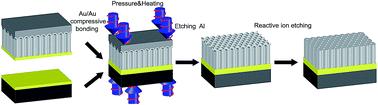
AAO membranes become essential for fabricating nano-building blocks. However, the integration of these nano-building blocks in complex machinery is still challenging, mainly due to the fragility of these membranes. In this work, we overcome this drawback by developing a new integrative process which enables the support of a highly-ordered nanoporous membrane onto a mechanically robust substrate such as silicon. The fabrication of supported AAO (SAAO) membranes is achieved by transferring an AAO layer onto a Si substrate via a Au/Au compressive bonding process. Two types of AAOs were prepared for this bonding process to demonstrate the universality of our technology: mild-anodized AAO (MA-AAO) and pulse-anodized AAO (PA-AAO). We also demonstrate that the newly developed SAAO membranes are suitable for electrodeposition of nanostructures. Problems such as membrane handling or electrolyte leakage occurring in conventional AAO membranes are avoided, so that Ni nanostructures with well-controlled dimensions and uniform lengths are obtained. The high-aspect ratio Ni nanostructures have the potential to be used in various applications, such as biosensing and energy storage.
Efforts have been pursued to eliminate the barrier layer without changing pore parameters. For example, a few studies have demonstrated a barrier layer thinning via electrochemical method until conduction is sufficient to perform electrodeposition.34–37 However, this method fails to avoid an inhomogeneous barrier thinning and a dendritic shape of nanopores at the bottom of ANMs.38
Here, we demonstrate for the first time the fabrication of supported AAO (SAAO) membranes with ultrahigh aspect ratio (A.R. ≈ 1600) nanopores achieved by transferring an AAO layer onto a Si substrate via a Au/Au compressive bonding process. The newly developed SAAO exhibits hexagonally well-ordered nanopores with ultrahigh aspect ratio on a mechanically robust substrate. The pore shape, size, and length can be easily tuned during anodization prior to the bonding process. As Au is used as the bonding layer, the pores can be readily filled by means of electrodeposition. As an example, Ni NWs were plated into our SAAO, using simple direct current (DC) plating technique at low current densities.
The fabrication process is depicted in Scheme 1. Experiments are detailed in ESI.† Briefly, AAOs were fabricated by two-step anodization from Al bulk sheets. To demonstrate the universality of our technology two types of AAOs were prepared: mild-anodized AAO (MA-AAO) and pulse-anodized AAO (PA-AAO). In the first case, the Al sheet is anodized in ‘self-ordering regimes’. The mild anodization results in highly-ordered packed pores whose diameters are kept constant along the long axis.29 In the latter case, pore diameter is modulated along the pore axis and is obtained by alternating mild anodization (MA, anodization at a range of potentials where the process is stable and self-ordered in a specific bath) and hard anodization (HA, stabilized anodization at a range of potentials higher than MA).3 Afterwards, the AAO templates are coated with Au via thermal evaporation and placed on a Au-coated Si chip with the Au layers facing each other. Next the Au/Au compressive bonding process is carried out, during which the Au layers of Si and AAO are bonded via diffusion of Au under high pressure and temperature. Finally, the aluminum remaining on top of the AAO is chemically removed and the pores are opened by RIE. The final supported membranes are denoted as MA-SAAO and PA-SAAO, respectively.
Fig. 1(a) shows a representative SAAO with ultrahigh aspect ratio nanopores (pore diameter 37 nm, length 60 μm, A.R. ≈ 1600) after the complete fabrication process. Since the Si substrate (3.5 cm × 3.5 cm) is slightly bigger than the Al foil (3 cm × 3 cm), the Au-coated chip is still exposed on the sides of the rectangular sample. The region of interest where AAO is formed is located in a circular area at the center of the sample. Fig. 1(b) and (c) are the top view SEM images of the MA-SAAO before and after RIE, respectively. Before etching the barrier layer (Fig. 1(b)), the shape of a hexagonally patterned-inverted concave structure corresponding to the barrier layer is observed with a measured interpore distance of ≈100 nm. Despite the high pressure bonding process (5 MPa), the fragile AAO is completely preserved. The non-anodized Al layer serves as a buffer layer, which prevents damage to the underlying AAO layer during bonding. After RIE, completely opened nanopores with well-defined hexagonal arrays are observed (Fig. 1(c)). The measured interpore distance was approximately 100 nm for the MA-SAAO sample, consistent with the value observed before etching. The advantage of the anisotropic RIE process over conventional wet chemical etching procedures is that it only opens the pores without affecting the original pore size.39 If larger pores are required, then a pore-widening based on wet chemical etching can be performed afterwards.
For PA-SAAOs a relatively less ordered barrier layer with an interpore distance of approximately 60 nm is observed. The less ordered pore arrangement is probably due to the growth of small pores at the domain boundary as marked by the blue arrows in Fig. 1(d). A high-speed growth rate of pores under HA pulse is responsible for this unstable pore growth.40 Additionally, unlike the MA-SAAO sample, microcracks on the PA-SAAO sample are observed (Fig. S1†). The origin of microcracks is from the PA process rather than the bonding process, as evidenced by a control experiment in which cracks are developed immediate after wet etching of Al substrate for a PA-AAO without bonding (Fig. S2†). The development of those microcracks is a consequence of releasing internal stress in the AAO when the Al substrate is removed. To minimize the internal stress, a constant interpore distance is prerequisite. A constant interpore distance can be achieved by applying a constant anodizing potential.5,6 However, this is demanding for pulse anodization because power supplies naturally exhibit a rising and falling time that prevents an ideal square pulse. The pores closed by the barrier layer can be opened with RIE without modifying pore diameter, as is observed in Fig. 1(e).
In order to reveal the features of the Si/Au/AAO multi-layer stacks, a deep trench was created through the surface of an SAAO membrane using a focused ion beam (FIB) milling process, and the resulting cross-section was imaged by SEM. Fig. 2(a) shows a well-bonded Au layer located between the Si and the AAO layer. While the smooth interfaces between different layers show that the bonding process is successful, the pores of AAO are damaged by the FIB milling even at a low ion dose (1 μA). To clearly reveal the feature of pores, the membrane is broken mechanically. The corresponding SEM image in Fig. 2(b) shows uniform vertically-aligned nanopores, which are directly in contact with the bonded Au layer.
![]() | ||
Fig. 2 The cross-sectional SEM images of SAAO with ultrahigh aspect ratio nanopores, obtained from a specimen prepared by a FIB (a), and a manual cleaving method (b). |
This membrane configuration exhibits several benefits over freestanding membranes and conventional SAAOs in terms of further electrodeposition. Compared to freestanding membranes, the Si substrate provides a mechanically robust support and prevents the rupture of the membrane. More importantly, unlike the pores of freestanding membranes that contain inhomogeneous tubular-shaped Au electrodes formed by sputtering, our SAAO contains a solid and flat Au electrode on a Si chip that completely seals the pore openings. This prevents the leakage of electrolyte from the nanopore during electrodeposition and helps obtain uniform NWs in length due to a more evenly-distributed current. For templates with unavoidable microcracks, e.g. the PA-AAO, this is especially important, because microcracks usually cause severe electrolyte leakage, which results in undesired deposition on the backside of the conductive layer and, thus, failure when electrodeposition is carried out in a PA-AAO membrane in its freestanding form.
The advantage of the newly developed SAAO membranes over conventional SAAOs is the absence of the barrier oxide layer at the conductive surface. Because of the high dielectric constant of the barrier, a high current density or potential is usually employed for electrodeposition, which frequently leads to porous nanostructures due to excessive hydrogen evolution.41 Moreover, finding an optimal current or potential is not straightforward because the thickness of the barrier layer varies as a function of the applied potential in the anodization process.13,42 For these reasons, the remaining barrier layer is commonly removed by wet chemical etching. However, wet etching results in an increase of the pore diameter due to its isotropic etching nature.1 In contrast, our SAAO membrane has the pre-opened pore side adhering on the Au conductive layer, and the barrier layer on the other side can be easily removed by RIE after bonding without influencing the pore parameters. Through this configuration, electrodeposition takes place directly on the Au conductive layer, enabling DC electrodeposition.
As a proof of concept, Ni was electrochemically deposited into the MA-SAAO template at a constant current density of −2 mA cm−2. The color of the AAO turned black, indicating a successful deposition of Ni throughout the template area (Fig. 3(a)). The cross-sectional SEM view of the MA-SAAO sample in Fig. 3(b) shows uniformly deposited Ni NWs inside the pores with an overall length of 5 μm. It is important to note that the uniform length was achieved because the nanopores were completely sealed by the Au contact layer. A back-scattered SEM image (Fig. 3(c)) shows Ni NW arrays standing on a Au/Si substrate after etching the AAO. The observed brighter regions correspond to the Au layer (due to its higher atomic number). The obtained freestanding high-aspect-ratio NW arrays have the potential to be used as building blocks for biosensors, batteries, solar cells and optical sensors.43–46 Fig. 3(d) shows a single uniform NW with a high-aspect ratio of above 130 (the diameter and the length are 37 nm and 5 μm, respectively).
Similarly, DC plating was also used for Ni deposition into PA-SAAO membranes at a constant low current density of −3 mA cm−2. Even though the AAO contained a microcrack as previously seen in Fig. S1,† Ni was still successfully electrodeposited in the AAO as shown in Fig. 4(a). A cross-sectional SEM image shows Ni NWs with an overall length of approximately 14 μm (Fig. 4(b)). The alternating MA and HA segments can be distinguished by the image contrast, which results from the difference of amount of Ni grown in the two segments. We note that deviation in length of HA segments is a general consequence of an unstable pore growth rate during HA pulses.47 For detailed observations, Ni NWs were released from the template by etching the AAO membrane in 5 M NaOH and further sonication. Fig. 4(c) shows a Ni NW bundle obtained from a PA-SAAO membrane. An SEM image with higher magnification (Fig. 4(d)) shows modulated diameter along the NW long axis. The observed segment diameters are 50 nm and 20 nm, which correspond to the pore sizes of the HA and MA regions, respectively.
Feasibility | Process | |||
---|---|---|---|---|
Conventional freestanding membrane | Thin Al deposited SAAO | Barrier layer thinned SAAO36 | SAAO with ultrahigh aspect ratio nanopores | |
a ○: feasible, ×: infeasible. | ||||
RIE process (for the smallest pore diameter) | ○ | × | × | ○ |
High aspect ratio nanopores | ○ | × | ○ (but with a dendritic pore shape) | ○ |
Two step anodization | ○ | × | ○ | ○ |
PA process | ○ | × | ○ | ○ |
A mechanically stable substrate | × | ○ | ○ | ○ |
Direct current plating at a low current density | ○ | × (feasible only after wet etching process) | × (remaining barrier layer with a thickness of a few nm) | ○ |
Uniformity of electrodeposition | × | ○ | ○ | ○ |
Footnote |
† Electronic supplementary information (ESI) available: Experimental details, SEM images and photos of cracks on PA-AAO. See DOI: 10.1039/c5ra20170e |
This journal is © The Royal Society of Chemistry 2015 |