
The disparate impact of two types of GMI effect definition on DC Joule-heating annealed Co-based microwires
Si-Da Jianga,
Da-Wei Xinga,
Wei-Dong Feia,
Jing-Shun Liub,
Hong-Xian Shena,
Wen-Bin Fangac and
Jian-Fei Sun*a
aSchool of Materials Science and Engineering, Harbin Institute of Technology, Harbin 150001, P. R. China. E-mail: jfsun@hit.edu.cn
bSchool of Materials Science and Engineering, Inner Mongolia University of Technology, Hohhot 010051, P. R. China
cSchool of Materials Science and Engineering, Harbin University of Science and Technology, Harbin 150080, P. R. China
First published on 10th November 2015
Abstract
Based on a comprehensive study of the effect of progressive DC Joule-heating annealing (DJA) on giant magneto-impedance (GMI) properties of melt-extracted amorphous microwires, we systematically analysed the different mechanisms for two types of GMI effect definition. Experimental results show that DJA can improve GMI response characteristics and magnetic field sensitivity (MFS) effectively for both definitions, but ΔZ/Z0 is enhanced much more than ΔZ/Zmax of the as-cast wires. At 20 MHz, the maximum GMI ratios, as denoted by ΔZ/Z0 and ΔZ/Zmax, of DJA microwires are enhanced to 582.59% and 639.13%, while the values for the as-cast wires are 69.09% and 520.48% respectively. Meanwhile, the MFS (ξmax) and equivalent magnetic anisotropy field (Hk) increase to 1346.4%/Oe (ΔZ/Z0), 2927.9%/Oe (ΔZ/Zmax) and 1.1 Oe, respectively. These significant effects of GMI properties as denoted by Z0 are mainly attributed to the change of resistivity (ρdc) for amorphous microwires induced by DJA. Revealing the mechanism of different effects can also result in the development of a micromagnetic field sensor, especially for geomagnetic sensor applications (∼±1.0 Oe).
Introduction
Recently, melt-extracted amorphous microwires have attracted much attention due to their various potential industrial applications, especially as giant magneto-impedance (GMI) sensor elements for detecting weak magnetic fields.1–4 Compared with other fabrication techniques including rotating-water and glass-covered spinning, melt-extracted microwires without a glass-covered coating exhibit a higher cooling rate, which results in better mechanical and magnetic properties, such as superior soft magnetic properties and large fracture strengths. This excellent performance makes melt-extracted microwires more suitable for applications in electronic packages and magnetic sensors, especially in GMI sensor elements. From previous work based on a great deal of related experiments conducted by our group, the parameters of melt-extraction can be accurately and effectively controlled, thus Co-based melt-extracted microwires with excellent GMI properties can be easily fabricated and used for designing sensors for detecting micromagnetic fields.5–7A key explanation of GMI effects is given by the well-known skin effect, which means AC current flows only in the outer region of magnetic amorphous wires at high frequency; on the other hand, with a higher frequency of AC, the effective conducting cross-section is almost limited. Remarkably, the impedance of amorphous wires will sharply change when an extra axial magnetic field (Hex) is applied, which influences the circumferential magnetization process under specific conditions. The skin effect is determined by the skin depth, as denoted by δ = (ρ/πfμφ)/2, where μφ is the circumferential direction magnetic permeability of the microwires, ρ is the electrical resistivity and f is the AC frequency.8–12 In general, there are two classic types of definition for quantitatively evaluating GMI effects that have been previously reported: one is quantitatively measured using Z0 (Hex = 0), the GMI ratio as denoted by ΔZ/Z0 is defined by eqn (1) as reported in ref. 13; the other is based on using Zmax (Hex = max), and the GMI ratio, as denoted by ΔZ/Zmax, is defined by eqn (2) as reported in ref. 14.
 | (1) |
 | (2) |
Commonly, melt-extracted microwires have a relatively large residual inner stress, which reduces their magnetic properties and GMI performances. Based on previous reports, the GMI response of sensitive materials can be optimized mainly through proper post-processing treatments. Lots of work has been done for enhancing GMI performance by annealing treatments: L. V. Panina et al.15 firstly reported the effect of tension annealing (TA) on amorphous microwires, for which the average change in the rate of voltage can reach 50%/Oe at 10 MHz. Moron et al.16 reported that vacuum annealing (VA) of Fe-based nanocrystalline microwires enhanced their magnetic properties; the GMI ratio increased from 1% for the as-cast microwires to 5% after VA treatment. Zhou et al.17 observed the effect of AC Joule-heating (AC) of melt-spun CoFeSiB amorphous ribbons on GMI properties, and [ΔZ/Z0]max was enhanced to about 180% at 900 kHz for 30 min with an AC current density of 2.8 × 10⁷ A m−2. V. Zhukova et al.18 reported that DC current annealing (DCA) with or without a DC axial magnetic field can significantly influence the magnetic properties of glass-coated microwires, and the obvious longitudinal magnetic anisotropy generated by the combined effects of the magnetic field and internal stresses arising from the coating during annealing. K. R. Pirota et al.19 found that DC Joule annealing (DJA) induced a short-range order relaxation that distinctly improved the soft magnetic properties of Co-based glass-coated microwires and enhanced [ΔZ/Zmax]max at 15 MHz to nearly 600% for the annealing conditions (10 min annealing and 70 mA). Regretfully, we are unable to make a complete list or comparison of post-treatments due to their diversity, and according to the above mentioned reports and the wire shape, Joule-heating annealing is probably a suitable method for post-processing of melt-extracted wires. Above all of these, researchers usually focus on one type of definition and try to establish a relationship between GMI effect and circumferential magnetic permeability.
In this paper, the effect mechanism of post-treatment on amorphous microwires was systematically studied based on two types of definition. We attempt a thorough quantitative analysis of the impedance of Co68.15Fe4.35Si12.25B14.25Zr1 melt-extracted amorphous microwires (defined herein as the research samples) with progressive DC Joule-heating annealing (DJA) to reveal the different change mechanisms induced by annealing of two types of GMI effect definition. Generally, the current annealing applied to different wires for the annealing time was under 600 s. Also, we chose one wire to anneal by step mode and the total annealing time could reach 50 min, which we have previously introduced, as detailed in our earlier published paper.20 This modified DJA effectively avoids experimental error and nonuniformity of different microwires during measurements, and as such we would obtain optimal magnetic properties, especially for the GMI ratio and MFS of sensitive materials. Moreover, Hk is enhanced to ∼1 Oe, which is an important figure for an application-oriented GMI sensor.
Experimental
A mother alloy ingot with a nominal composition of Co68.15Fe4.35Si12.25B14.25Zr1 (in at%) was firstly prepared using arc-melting in pure argon and copper mould casting methods. During a melt-extraction process, the mother alloy was re-melted in a Boron Nitride (BN) crucible by an induction coil and extracted by the edge of a high-speed rotating Cu wheel in purified argon; the schematic diagram is also shown in our previous reports.20The obtained wires possess diameters ranging from 20 to 100 μm and saturated magnetostriction with nearly a small negative value (nearly |λs| ≤ 10−6).21 A uniform and continuous wire with a diameter of ∼42 μm was selected and post-processed by DJA, with currents ranging from 60 mA (nearly equal to 4.33 × 10⁷ A m−2) to 120 mA (nearly equal to 8.66 × 10⁷ A m−2), the step value was set as 20 mA and the annealing time was 600 s for each stage.20 The impedance of the wire was measured using an Agilent 4294A precision impedance analyzer, whose frequency of driving current was varied from 0.1–20 MHz and amplitude of driving current was kept at 20 mA; resistivity was measured using an Agilent 4339B and the length of the sample was 26 mm when connected by Cu clamping apparatus. It was placed in a pair of Helmholtz coils parallel to the axis of the wire to avoid the disturbance of the geomagnetic field. The DC magnetic field sensitivity ξ of GMI can be expressed as follows:
 | (3) |
 | (4) |
The structural information of the as-cast wires was determined by X-ray diffraction with Cu Kα radiation (XRD, Rigaku D/max-γ B) and scanning electron microscopy (SEM, Hitachi S-4700). In addition, the microstructure of the as-cast and annealed wires was examined by high-resolution transmission electron microscopy (HRTEM, Tecnai G2F30) and the steps for HRTEM sample preparation are shown in ref. 22. The measurement of magnetic properties was carried out on a vibrating sample magnetometer (VSM, Lake Shore 7410).
Results and discussion
Fig. 1 shows the XRD pattern and SEM image of an as-cast microwire. The XRD pattern displays a broad diffuse diffraction maximum. This evidence directly indicates that the as-cast microwires mainly consist of an amorphous phase. The diameter of the wire is ∼42 μm and the surface of the wire is quite smooth as shown in the SEM image (Fig. 1). Almost no macro Rayleigh wave defects were observed in the SEM image. However, there exists a groove on the wire which is induced due to surface contact between the melt puddle and the quenching Cu wheel during the course of fabrication.20 Relatively, more smooth and no obvious defects are conducive to achieving an excellent GMI property.23,24 | ||
| Fig. 1 XRD pattern and inset SEM image of the as-cast microwire. | ||
Then we measured the GMI effects for both the as-cast and post-treatment wires. Fig. 2 shows the change in the GMI ratio profiles of the as-cast and variation tendency of DJA-ed microwires with Hex in a different current intensity range of 60–120 mA at 20 MHz, concentrated on the different definitions given by eqn (1) & (2), respectively. Note that the ratio defined by ΔZ/Z0 is enhanced when the annealing current intensity is increased from 60 (nearly equal to 4.33 × 10⁷ A m−2) to 80 mA (nearly equal to 5.76 × 10⁷ A m−2) and then reduced as the current density continues to increase. [ΔZ/Z0]max can reach 582.59% at 80 mA and is enhanced nearly 8.4 times compared with the value for the as-cast wires of 69.09%. Correspondingly, the behaviour of the GMI ratio defined by ΔZ/Zmax shows a similar tendency to increase at first and then decrease with an increased annealing current, but the [ΔZ/Zmax]max improved from 520.89% for the as-cast wire to 639.13% after annealing at 60 mA. The insets clearly show the GMI ratios at weak external magnetic fields. We can therefore evaluate GMI effects at different annealing current density stages using different definitions, which show various characteristics for designing new sensors. At Hex = 0 Oe, all curves show different starting points for ΔZ/Zmax as shown in the inset of Fig. 2b, and on the contrary these curves show the same start values for ΔZ/Z0 in the inset of Fig. 2a.
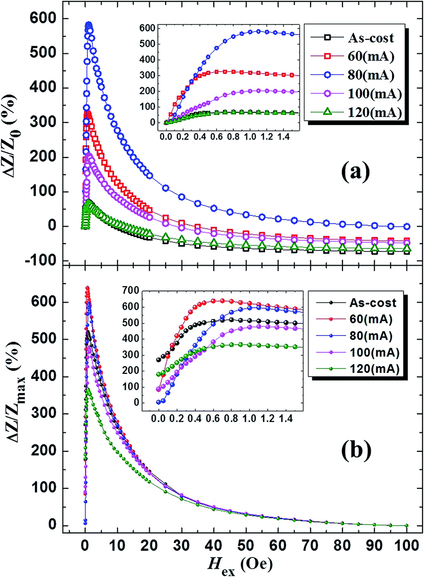 | ||
| Fig. 2 The change in the GMI ratio curves of the as-cast and variation tendency of DJA-ed microwires with Hex in a different current intensity range of 60–120 mA at 20 MHz, (a) defined by Z0 (Hex = 0 Oe), the enlarged inset shows the tendency in a weak external magnetic field (0–1.5 Oe), and (b) defined by Zmax (Hex = 100 Oe). | ||
Obviously, we confirmed that the better parameters of the DJA method for obtaining quantitative values of GMI effects are 80 mA and 60 mA for ΔZ/Z0 and ΔZ/Zmax, respectively, as shown in Fig. 2a and b. Thus we show the field dependence of GMI curves in detail at selected frequencies from 0.1–20 MHz at the annealing stages (a) 80 mA for 600 s (ΔZ/Z0) and (b) 60 mA for 600 s (ΔZ/Zmax) of a single microwire in Fig. 3. Basically, GMI ratio curves sequentially increase with different driving frequencies for both definitions in Fig. 3a and b. At f ≥ 13 MHz, the value of the ratio exceeds 500% after 80 mA annealing for the ΔZ/Z0 definition as shown in the inset of Fig. 3a. The threshold value of driving frequency decreases to 5 MHz for 60 mA (ΔZ/Zmax). The GMI profiles illustrate the high sensitivity of impedance for the ΔZ/Z0 definition when Hex ≤ 1.1 Oe as seen in the inset of Fig. 3a and for the ΔZ/Zmax definition when Hex ≤ 0.7 Oe. All the GMI curves exhibit a single-peak feature at f ≥ 0.1 MHz for both GMI definitions. This remarkable behavior has potential applications in GMI sensors for weak field detection,14 especially for those requiring small bias fields and high sensitivity such as biomagnetic and geomagnetic detection. Another noticeable feature is that the GMI curves at different frequencies show almost linear changes to the magnetic field from 1.1–50 Oe for the ΔZ/Z0 definition and 0.7–40 Oe for the ΔZ/Zmax definition as shown in Fig. 3a and b, respectively, which display a wider range of external fields for detecting a larger bias field with high sensitivity. Therefore, high sensitivity to a weak magnetic field and a linear response to a larger magnetic field mean that this post-treated microwire can be exploited for double functional GMI sensor applications.24
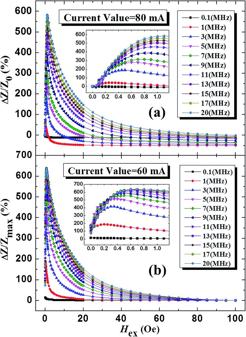 | ||
| Fig. 3 Field dependence of GMI profiles at selected frequencies between 0.1–20 MHz at different annealing stages, (a) 80 mA for 600 s (ΔZ/Z0), and (b) 60 mA for 600 s (ΔZ/Zmax) of a single microwire. The magnified insets of the curve linear increase field response at working ranges (0–1.1 Oe). | ||
Magnetic field sensitivity decides the intrinsic response speed of a GMI sensitive material, so it acts as the decisive design parameter for a sensor. Fig. 4 illustrates respectively magnetic field sensitivity (ξmax) and [ΔZ/Z]max as functions of annealing current densities by different definitions. From the above images, the maximum GMI ratio [ΔZ/Z]max and ξmax%/Oe obviously change with the amplitude of the annealing current and they have similar salient values and have a tendency to jump. After 60 mA annealing, ξZmax and [ΔZ/Zmax]max reach 2927.9%/Oe and 639.13%, respectively, meanwhile ξZ0 and [ΔZ/Z0]max reach a largest value of 1346.4%/Oe and 582.59% respectively at 80 mA annealing. These magnetic field sensitivities ξZmax and ξZ0 are bigger than those of most amorphous wires mentioned in ref. 1. Measured using different modes, ξ and ΔZ/Z possess dissimilar starting thresholds and dramatically decrease when surpassing the threshold value. So, we obtained an excellent and specific performance of ξ corresponding to driving frequency at a diverse threshold in Fig. 5. Both of them have a tendency to be sharply enhanced at f ≤ 5 MHz, then to decline and remain almost constant. In all tests of frequency domain, all values of ξZmax are higher than those of ξZ0.
 | ||
| Fig. 4 (a) Magnetic field sensitivities ξmax and (b) GMI ratios [ΔZ/Z] of Hk by different definition modes change with different annealing current densities. | ||
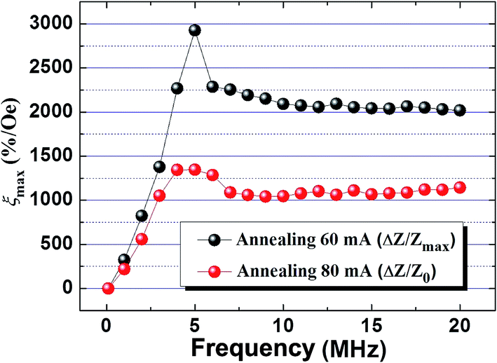 | ||
| Fig. 5 Magnetic field sensitivity ξmax of the ideal annealing stage depends on the frequency defined by Zmax and Z0. | ||
The working magnetic field and frequency are equally important factors for sensor applications, usually for weak field detecting sensors, and the working field range means the equivalent anisotropy field Hk, which is the corresponding magnetic field of the maximum GMI ratio. Fig. 6 shows the equivalent anisotropy field (Hk) dependence of frequency for DJA current amplitudes of 60–120 mA and a dotted box corresponding to the highest ratios at 20 MHz. After annealing, all curves of Hk show a staircase-like enhancement with increasing frequency. This is due to their enhancement of eddy current damping, which means more external magnetic field energy is needed for domain wall motion and domain rotation to occur. With an increase in annealing current density, the variation trend of Hk gradually improves. For the 60 mA annealing stage, the curve of Hk remains unchanged compared with that of the as-cast state. When the annealing current is increased to 80 and 100 mA, Hk is observed to improve for the full frequency selection and reaches 1.1 Oe at 20 MHz. Then with a continued increase of annealing current density, Hk shows a slight fluctuation, but it then nearly reaches a saturation value. Accordingly, the definition of the mentioned weak field detection sensor working range (including frequency and magnetic field) means a large [ΔZ/Z0]max and ξmax and a small Hk, at relatively low frequency, especially DJA-ed wire (80 mA, as defined by eqn (1)) with a significantly larger [ΔZ/Z0]max and ξmax and a relatively smaller Hk at 12–20 MHz, which will be more suitable and favorable for practical sensor applications, especially for weak magnetic field detection, owing to the small biased magnetic field and power loss.
 | ||
| Fig. 6 Statistical diagram of the equivalent anisotropy field Hk dependence of frequency under different annealing current amplitudes of DJA and a dotted box corresponding to the highest ratio at 20 MHz. | ||
Fig. 7 displays the longitudinal magnetic hysteresis (M–H) loops of the as-cast and DJA-ed (denoting annealing at 80 mA for 600 s) Co-based microwires and the inset shows the image at the magnified central area. Both as-cast and DJA-ed microwires exhibit typical features of magnetic bistability with nearly negligible hysteresis. And the magnetizations achieved their saturation state at a relatively low external magnetic field. It also indicates a reduction trend of the longitudinal saturation magnetization Ms and longitudinal permeability after DJA treatment (Ms decreases from 67.32 emu g−1 for the as-fabricated to 61.66 emu g−1 for the DJA-ed wire), also the hysteresis narrows down as displayed in the inset of Fig. 7. A negative, near zero magnetostriction coefficient of Co-based amorphous microwires is displayed by magnetic domain structures in the axial (or longitudinal) and circumferential directions.25,26 The volume fraction of the circumferential magnetic domain increases owing to the circumferential magnetic field generated by the annealing current. Accordingly, the volume fraction of the axial magnetic domain decreases synchronously. Herein, it can also be seen that circumferential anisotropy further increased the Hk and reduced the included angle between the axial direction of magnetization and the circumferential (Ψ).27 Structural relaxation and release of residual internal stress can effectively recede the coercivity (Hc) thus further forming narrow hysteresis loops.28 Hk raises the difficulty of easy axis magnetization then causes lower longitudinal permeability. In conclusion, these changes in magnetic properties induced by DJA show the improvement of the GMI performances.
 | ||
| Fig. 7 Magnetic hysteresis (M–H) loops, and magnified central region (inset) of as-cast and 80 mA DJA-ed microwires. | ||
From a microstructural perspective and as shown in previous work,29 magnetic properties are closely related to the microstructure of amorphous microwires. High-resolution transmission electron microscopy (HRTEM) analyses and selected area electron diffraction (SAED) were employed to investigate the microstructures of the as-cast and DJA-ed wires. Inverse fast Fourier transform (IFFT) and autocorrelation function (ACF) methods were used to provide more direct evidence to establish the corresponding relationship between microstructure variation and GMI effect. Fig. 8 displays the HRTEM images and SAED patterns of the studied microwires and the corresponding local magnification. The SAED pattern of the DJA-ed microwire (Fig. 8e) displays crystalline diffraction light-spots and the SAED image of the as-cast microwire (Fig. 8b) only displays classic amorphous diffraction rings, which indicate the presence of a large amount of nanocrystalline material. Generally, an ACF technique with reference to microstructural information was applied to quantitatively identify and calculate the degree of nanocrystallization on a selected micro-area of the as-cast and DJA-ed microwires.30 The detailed process of the ACF technique includes the following steps: firstly, the HRTEM image was divided into 64 sub-images with a uniform area of 18 nm2, and one sub-image, e.g. with coordinates of (→5, ↓6) in Fig. 8c, which expresses distinct crystal-like diffraction fringes in its ACF patterns was chosen as a reference pattern to depict nanocrystallization in this work. Next, other sub-images that exhibit clearer and more uniform fringes than the reference pattern were considered to be nanocrystalline. Statistical analysis of all the small selected areas reveals that the degrees of nanocrystallization shown in Fig. 8a and (d) are 6.25% and 32.81%, respectively. Nanocrystals appear on the amorphous matrix in the as-cast microwires, which may be induced during the process of fabrication, and the degree is relative to the technological parameters.31 A comparative IFFT study of regions 1# and 2# in (b) and 3# and 4# in (e), indicates that the arranged atomic micro-regions change more regularly.22 Apparently, DJA treatment gives a remarkable enhancement in the degree of nanocrystallization. Formation of nanocrystalline material (in terms of the degree of nanocrystallization with the ACF technique) is due to the diffusion and rearrangement of atoms which are induced by the co-actions of thermal activation energy and circular magnetic-field energy during the DJA process. DJA can both release inner residual stress and improve structural relaxation properly. It is well known that Joule-heat treatment will reduce the concentration of free volume and defects further to properly reduce the magnetoelastic coupling effect, thus will enhance the permeability (also known as circumferential permeability) which can improve the GMI effect. In addition, it also can effectively regulate the distribution of a circular magnetic anisotropy domain, which is considered to be the reason for the self-generation of an external circular magnetic field during the annealing process.14 Meanwhile the release of inner residual stress and relatively higher degree of nanocrystallization can obviously reduce the resistivity of DJA-ed microwires, which is another important influential factor for GMI effects.
 | ||
| Fig. 8 HRTEM images of the as-cast (a) and DJA-ed 80 mA (d) amorphous microwire with nanocrystalline material (region 1#, 2#, 3#, 4#). (b) and (e) show SAED patterns of the corresponding whole areas; the two lower pictures show the inverse fast Fourier transform (IFFT) patterns of areas 1# and 2# marked by a blue frame in (a) and 3# and 4# in (d). (c) and (f) show the autocorrelation function (ACF) of the HRTEM images. | ||
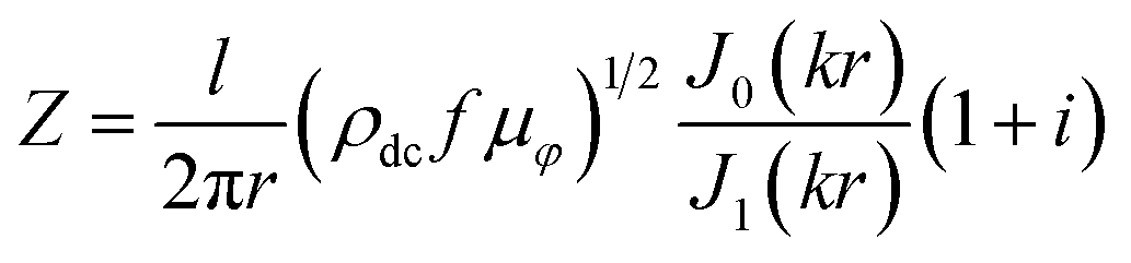
Fig. 9 illustrates the impendences at different external magnetic fields (Hex = 0, Hex = 100 Oe, Hex = Hk), resistance (R0) and reactance (X0) separation of Z0 (Fig. 9b). The inset of Fig. 9b shows the DC resistivity (ρdc, at room temperature) dependence with an annealing current value of 20 MHz. We indicated that the Z0 decline with annealing stage then increases after a threshold value (corresponding to 80 mA) while the Zmax remains essentially constant, but the ZHk shows a slight increase then a sharp decrease. Maximum values of Δ[Z − Z0] and Δ[Z − Zmax] are respectively reached with 80 mA and 60 mA annealing stages then decrease gradually as shown in Fig. 9a. The R0 and X0 separation of Z0 (Fig. 9b) and DC resistivity (inset of Fig. 9b) curves show the same trend with Z0. Most previous research on current annealing has focused on the enhancement of GMI effects owing to a change of ZHk, however, herein we attempted to analyze a more important influence which is the variation of Z0. Based on the Maxwell equation and ignoring the Landau–Lifshitz equation, in an amorphous microwire, Z can be expressed by:15
 | (5) |
 | ||
| Fig. 9 (a) Impendences at different external magnetic fields (Hex = 0, Hex = 100 Oe, Hex = Hk), (b) resistance, R0, and reactance, X0, separation of Z0, the inset of (b) shows the DC resistivity dependence with an annealing current value of 20 MHz. | ||
Actually, Z0 means the impedance of alternating current inside the microwire without Hex. So, it is only related to the circumferential magnetization process induced by AC without axial magnetization. The change of R0 is more intense and shows a higher value than X0 as shown in Fig. 9b. Obviously, the variation trend of the resistivity ρdc induced by DJA becomes the main decisive factor governing the Z0 value. The release of inner residual stress induces structural relaxation and increases the degree of nanocrystallization during the annealing process; these factors decide the trend of ρdc. With the appearance of nanocrystallinity during the annealing stage (as seen in Fig. 8e), ρdc will show an irreversible breakdown.32 According to the generalized Ziman theory by Nagel about liquid metal, electron scattering mainly depends on the relative location of the first peak between a Fermi surface and structure factor. The disordered structure of the amorphous alloy is centered around electron scattering, as the structural relaxation and nanocrystallinity generated by DJA can effectively decrease ρdc. But with the accumulation of DJA (maybe more than the threshold), then ρdc visibly increases. Based on different mechanisms of scattering, there are two types of material resistance: one is phonon scattering induced by thermal vibrations of lattice atoms, this resistance is usually associated with temperature (ρt); another is the perspective of flaw scattering, this will not change with practical temperatures, and the temperature coefficient of resistance (TCR) has a small value.33 We hold the opinion that dispersion of the nanocrystalline phase will enhance the TCR and increase the level of the heat eddying effect, then the co-action improves ρdc at 20 mA AC of impedance tests. In the meantime, three-dimensional nanocrystalline growth will change the stress state of the microwire, which can further increase ρdc at room temperature. The variation tendency of Zmax and ZHk is decided by a dynamic axial magnetization process, so circumferential permeability can be the major influential factor. At Hex = Hk, domain wall movement and domain rotation together determine the μφ and then reach a maximum value. But with Hex continuously increasing (which is bigger than Hk), the axial direction is a difficult magnetization direction for the circumferential magnetic domain, so domain rotation is gradually inhibited. When the Hex increases to 100 Oe, the domain basically does not rotate which means that μφ is almost invariant even after DJA treatment. Therefore the tendency of Zmax shows a small change as shown in Fig. 9a. For the stage of DJA (both 60 and 80 mA), at the beginning the value of μφ was enhanced slightly, then decreased with an increase in annealing current. The greater nanocrystallity will generate a pinning effect which can hinder the movement of the domain wall and strengthen eddy current damping further to decrease the value of μφ. All of the above make the curve of ZHk just like those shown in Fig. 9a.
Overall, through quantitative description of impedance for as-cast and DJA microwires, we demonstrate the different mechanisms of two GMI effect definitions. Such different mechanisms of DJA post-treatment can be concluded as follows: the enhancement of Δ[Z − Z0]/Z0 results from the marked decline of Z0 and improvement of ZHk; and Δ[Z − Zmax]/Zmax only depends on the increase of ZHk. DJA treatment plays a more effective role for the enhancement of Δ[Z − Z0]/Z0 than Δ[Z − Zmax]/Zmax. The GMI effect defined by Zmax is enhanced slightly, but it displays excellent ξZmax rather than ξZ0. Thus, we can choose the most fitting definition mode for practical application for magnetic sensors and provide novel design ideas.
Conclusions
DJA at 60 mA and 80 mA has a relatively remarkable effect on the GMI effect: two mainly different indexes, [ΔZ/Zmax]max and [ΔZ/Z0]max, increase to 639.13% and 582.59%, and the maximum values of ξZmax and ξZ0 increase to 2927.9%/Oe and 1346.4%/Oe, respectively. Meanwhile, the MFS is enhanced to 1.1 Oe at 20 MHz. Overall, through a quantitative description of impedance for the as-cast and DJA microwires, we demonstrate the different effects of the mechanism with two GMI definitions. Therefore, DJA can be used to enhance the GMI effect of amorphous microwires for high-performance sensor applications. In conclusion, we can choose different annealing processes and their corresponding definition modes as the basis of a practical working environment for the rational design of GMI sensors.Acknowledgements
This work was financially supported by the National Natural Science Foundation of China (NSFC) under grant No. 51371067. J. S. L. acknowledges the National Natural Science Foundation of China (NSFC) under grant No. 51401111 and 51561026, and the Natural Science Foundation of Inner Mongolia Autonomous Region of China under grant No. 2014BS0503.References
- M. H. Phan and H. X. Peng, Giant magnetoimpedance materials: Fundamentals and applications, Prog. Mater. Sci., 2008, 53, 323–420 CrossRef.
- M. Knobel and K. R. Pirota, Giant magnetoimpedance: concepts and recent progress, J. Magn. Magn. Mater., 2002, 242(1), 33–40 CrossRef.
- J. S. Liu, J. F. Sun, D. W. Xing, X. Xue, S. L. Zhang, H. Wang and X. D. Wang, Experimental study on the effect of wire bonding by Cu electroplating on GMI stability of Co-based amorphous wires, Phys. Status Solidi A, 2011, 208, 530–534 CrossRef CAS.
- H. Chiriac, M. Tibu and V. Dobrea, Magnetic properties of amorphous wires with different diameters, J. Magn. Magn. Mater., 2005, 290(2), 1142–1145 CrossRef.
- P. Ciureanu, I. Khalil, L. G. C. Melo, P. Rudkowskib and A. Yelona, Stress-induced asymmetric magneto-impedance in melt-extracted Co-rich amorphous wires, J. Magn. Magn. Mater., 2002, 249, 305–309 CrossRef CAS.
- F. X. Qin, Y. Quéré, C. Brosseau, H. Wang, J. S. Liu, J. F. Sun and H. X. Peng, Two-peak Feature of the Permittivity Spectra of Ferromagnetic Microwire/Rubber Composites, Appl. Phys. Lett., 2013, 102, 122903 CrossRef.
- H. Wang, F. X. Qin, D. W. Xing, F. Y. Cao, H. X. Peng and J. F. Sun, Fabrication and Characterization of Nano/Amorphous Dual-phase Finemet Microwires, Mater. Sci. Eng., B, 2013, 178(20), 1483–1490 CrossRef CAS.
- R. Varga, Y. Kostyk, A. Zhukov and M. Vázquez, Single domain wall dynamics in thin magnetic wires, J. Non-Cryst. Solids, 2008, 354, 5101–5103 CrossRef CAS.
- V. Zhukova, A. Zhukov, K. García, V. Kraposhind, A. Prokoshind, J. Gonzaleza and M. Vázquez, Magnetic properties and GMI of soft melt-extracted magnetic amorphous fibers, Sens. Actuators, A, 2003, 106, 225–229 CrossRef CAS.
- M. Vázquez, Soft magnetic wires, Phys. B, 2001, 299, 302–313 CrossRef.
- H. Chiriac and T. A. Óvári, Novel trends in the study of magnetically soft Co-based amorphous glass-coated wires, J. Magn. Magn. Mater., 2011, 323, 2929–2940 CrossRef CAS.
- F. X. Qin, J. Tang, V. V. Popov, J. S. Liu, H. X. Peng and C. Brosseau, Influence of Direct Bias Current on the Electromagnetic Properties of Melt-extracted Microwires and Their Composites, Appl. Phys. Lett., 2014, 104(1), 012901 CrossRef.
- J. F. Hu, H. W. Qin, F. Zhang and R. K. Zheng, Diameter dependence of the giant magnetoimpedance in hard-drawn CoFeSiB amorphous wires, J. Appl. Phys., 2002, 91, 7418–7420 CrossRef CAS.
- J. S. Liu, F. X. Qin, D. M. Chen, H. X. Shen, H. Wang, D. W. Xing, M. H. Phan and J. F. Sun, Combined Current-Modulation Annealing Induced Enhancement of Giant Magnetoimpedance Effect of Co-rich Amorphous Microwires, J. Appl. Phys., 2014, 115(17), 17A326 CrossRef.
- V. Panina and K. Mohri, Effect of magnetic structure on giant magneto-impedance in Co-rich amorphous alloys, J. Magn. Magn. Mater., 1996, 157/158, 137–140 CrossRef.
- C. Moron and A. Garcia, Giant magneto-impedance in nanocrystalline glass-covered microwires, J. Magn. Magn. Mater., 2005, 290, 1085–1088 CrossRef.
- X. Z. Zhou, G. H. Tu, H. Kunkel and G. Williams, Effect of Joule-heating annealing conditions on giant magnetoimpedance of Co-rich amorphous ribbons, Sens. Actuators, A, 2006, 125, 387–392 CrossRef CAS.
- V. Zhukova, A. F. Cobeño, A. Zhukov, J. M. Blanco, S. Puerta, J. Gonzalez and M. Vázquez, Tailoring of magnetic properties of glass-coated microwires by current annealing, J. Non-Cryst. Solids, 2001, 287, 31–36 CrossRef CAS.
- K. R. Pirota, L. Kraus, H. Chiriac and M. Knobel, Magnetic properties and giant magnetoimpedance in a CoFeSiB glass-covered microwire, J. Magn. Magn. Mater., 2000, 221, 243–247 CrossRef.
- S. D. Jiang, D. W. Xing, J. S. Liu, H. X. Shen, D. M. Chen, W. B. Fang and J. F. Sun, Influence of microstructure evolution on GMI properties and magnetic domains of melt-extracted Zr-doped amorphous wires with accumulated DC annealing, J. Alloys Compd., 2015, 644, 180–185 CrossRef CAS.
- H. Wang, F. X. Qin, D. W. Xing, F. Y. Cao, X. D. Wang, H. X. Peng and J. F. Sun, Relating Residual Stress and Microstructure to Mechanical and Giant Magneto-impedance Properties in Cold-drawn Co-based Amorphous Microwires, Acta Mater., 2012, 60(15), 5425–5436 CrossRef CAS.
- J. S. Liu, F. Y. Cao, D. W. Xing, L. Y. Zhang, F. X. Qin, H. X. Peng, X. Xue and J. F. Sun, Enhancing GMI Properties of Melt-extracted Co-based Amorphous Wires by Twin-zone Joule Annealing, J. Alloys Compd., 2012, 541, 215–221 CrossRef CAS.
- D. M. Chen, D. W. Xing, F. X. Qin, J. S. Liu, H. X. Shen, H. X. Peng, H. Wang and J. F. Sun, Cryogenic Joule annealing induced large magnetic field response of Co-based microwires for giant magneto-impedance sensor applications, J. Appl. Phys., 2014, 116, 053907 CrossRef.
- D. M. Chen, D. W. Xing, F. X. Qin, J. S. Liu, H. Wang, X. D. Wang and J. F. Sun, Correlation of Magnetic Domains, Microstructure and GMI Effect of Joule-annealed Melt-extracted Co68.15Fe4.35Si12.25B13.75-Nb1Cu0.5 Microwires for Double Functional Sensors, Phys. Status Solidi A, 2013, 210(11), 2515–2520 CrossRef CAS.
- L. V. Panina, K. Mohri, K. Bushida and M. Noda, Giant magneto-impedance and magneto-inductive effects in amorphous alloys (invited), J. Appl. Phys., 1994, 76, 6198 CrossRef CAS.
- M. Vazquez and A. Hernando, A soft magnetic wire for sensor applications, J. Phys. D: Appl. Phys., 1996, 29, 939–949 CrossRef CAS.
- M. Takajo, J. Yamasaki and F. B. Humphrey, Domain observations of Fe and Co based amorphous wires, IEEE Trans. Magn., 1993, 29, 3484–3486 CrossRef.
- K. Mohri, K. Bushida, M. Noda, H. Yoshida, L. V. Panina and T. Uchiyama, Magneto-Impedance Element, IEEE Trans. Magn., 1995, 31, 2455–2460 CrossRef.
- H. X. Peng, F. X. Qin, M. H. Phan, J. Tang, L. V. Panina, M. Ipatov, V. Zhukova, A. Zhukov and J. Gonzalez, Co-based magnetic microwire and field-tunable multifunctional macro-composites, J. Non-Cryst. Solids, 2009, 355, 1380–1386 CrossRef CAS.
- J. S. Liu, H. X. Shen, D. W. Xing and J. F. Sun, Optimization of GMI properties by AC Joule annealing in melt-extracted Co-rich amorphous wires for sensor applications, Phys. Status Solidi A, 2014, 211(7), 1577–1582 CrossRef CAS.
- F. X. Qin, Y. Quéré, C. Brosseau, H. Wang, J. S. Liu, J. F. Sun and H. X. Peng, Two-peak feature of the permittivity spectra of ferromagnetic microwire/rubber composites, Appl. Phys. Lett., 2013, 102, 122903 CrossRef.
- N. Banerjee, R. Roy and A. K. Majumdar, Electrical resistivity in the Fe100−xBx series (13 ≤ x ≤ 26), Phys. Rev. B: Condens. Matter Mater. Phys., 1981, 24, 6801–6806 CrossRef CAS.
- P. Peng, R. S. Liu and Q. Quan, The effect of high content of metalloid on resistivity and temperature coefficient of resistivity of amorphous TM-M alloys, Mater. Sci. Eng., B, 1996, 38, 62–64 CrossRef.
| This journal is © The Royal Society of Chemistry 2015 |