DOI:
10.1039/C5RA19542J
(Paper)
RSC Adv., 2015,
5, 93180-93186
Hyperbranched self-assembled photoanode for high efficiency dye-sensitized solar cells†
Received
22nd September 2015
, Accepted 23rd October 2015
First published on 23rd October 2015
Abstract
The photoanode morphology is key for improving photovoltaic performance of dye-sensitized solar cells. On one side, light harvesting depends on its capability of both chemisorbing high quantity of dye and affecting the flow of light in order to enhance its optical thickness. On the other, electron transport is influenced by the crystalline domain size and shape. In this work we report on how the morphology of self-assembled hyperbranched quasi 1D nanostructures can be engineered by physical vapour deposition in order to maximize light harvesting and electron transport. High specific surface area was achieved by optimizing crystalline domain size. This way, quasi 1D nanostructures allow for high light harvesting efficiency, broadband and intense light scattering while sustain significant decrease in electron transport time. Hyperbranched nanostructures photoanodes led to a power conversion efficiency over 9%.
Introduction
Dye-sensitized solar cells (DSC) are energy conversion devices using dye molecules capable of generating electron–hole pair upon light illumination. Despite the fact that the actual light harvesting is inherent in the dye molecules themselves, the device operation strongly relies on the TiO2 scaffold onto which these molecules are chemisorbed. Indeed, the mesoporous layers not only offer a high surface area rich of anchoring sites for the dye molecules but also work as charge collectors for photogenerated electrons towards the photoanode and thus the external circuit. This scaffold can be nanostructured to gain additional functionality and mold light propagation eventually leading to an intensification of the light–matter interaction. For this reason several studies have focused on novel nanostructures with the aim of enhancing the overall power conversion efficiency (PCE) through (i) the enhancement of light–matter interaction and (ii) improvement of electron transport.1,2 A possible route to light–matter interaction is to use additional nanostructures with dimension in the range of hundreds of nanometers as scattering element and thus enhancing the device optical thickness.3–5 The most exploited method, due to its easy fabrication, consists in the deposition of a scattering layer on top of the standard transparent mesoporous TiO2.6–8 Despite power conversion efficiencies above 10% have been achieved with these structures,9–11 low surface to volume ratio is reducing dye uptake on the TiO2 scattering overlayer.6 Moreover with this strategy electron transport is still left to the standard mesoporous layer which, given its randomly placed nanoparticles morphology, is far from optimal. Several photoanodes comprising elongated nanostructures as dye scaffold have been proposed as viable solutions to enhance light scattering and improve electron transport12 through channelled conduction of photogenerated charges along the main structural direction.13–15 As one-dimensional (1D) nanostructures, such as nanotubes or nanowires, present fairly low surface area compared to mesoporous counterparts, several studies have been done in order to enhance dye loading capability either through the creation of nanoboundles16 or through decoration of elongated structures with smaller structures. In a typical two-step process a previously grown film of 1D structures is decorated by either nanoparticles or by other smaller 1D structures in a hierarchical fashion.17–22 In this respect, in a previous publication we fabricated hierarchical tree-like nanostructure for liquid electrolyte DSCs coupling preferential direction and high surface area and that could reach an overall power conversion efficiency of about 5%.15 Despite morphological properties are crucial in order to improve light management and electron transport, the crystallinity of the TiO2 is another factor to consider when optimizing electron transport. One-dimensional structures do offer preferential pathways, however the presence of interfaces between small crystalline domains along this structures can still offer recombination sites that hamper electrons transport. With a multi-step solution based process, Wu et al.,23–25 fabricated elongated nanostructures with omnidirectional scattering properties, achieving a PCE of about 9% in liquid electrolyte devices. Similarly in a previous publication26 we demonstrated how a photoanode made of TiO2 hyperbranched quasi 1D nanostructures self-assembled from gas phase fabricated by pulsed laser deposition (PLD) led to a significant performance improvement in solid state DSCs compared with reference devices employing a standard mesoporous photoanode. This result was due to a combination of higher photocurrent generation, due to a higher optical thickness induced by light scattering, and also to faster charge transport in the hyperbranched quasi 1D nanostructures compared to standard mesoporous structures. In the present work, we report on similar nanostructures optimized for liquid dye sensitized solar cells. Here we show how the interplay of crystalline domain size and dye uptake of TiO2 hyperbranched quasi 1D nanostructures can be controlled to achieve high power conversion efficiency. Pulsed laser deposition grown hierarchical nanostructures turn hyperbranched in an energy minimization process during annealing. Through a fine optimization of this process, the modifications of crystalline domain size and roughness factor can be used to affect the volume to surface ratio of the crystals forming the nanostructures. In an optimized hyperbranched photoanode, the large surface area provides high dye uptake and strong broadband light scattering, allowing high photocurrent generation whilst the large anisotropic crystals fosters fast electron transport. Nevertheless it is shown that the growth of thick photoanodes does not guarantee a linear increase in photocurrent generation as the liquid electrolyte does not infiltrate across the top part of thick films. Overall, the characteristic of the optimized photoanode allows the achievement power conversion efficiency over 9%.
Results and discussion
Material characterization
In pulsed laser deposition, as described also in previous works,15,26 a focused excimer laser pulse (namely KrF with λ = 248 nm, 20 ns) ablates, within a vacuum chamber partially filled with a selected gas, a solid target of bulk material. After the laser–target interaction a nanoparticle inseminated plasma is formed and it expands towards the sample (s) placed face-on to the target (t) (distance t − s = 5 cm). In the case of TiO2, it was demonstrated that by setting specific background gas pressure in the deposition chamber, it is possible to achieve quasi 1D hierarchical structures with high specific surface area.26 Upon thermal treatment, above 350–400 °C (ref. 27) the nanostructures reorganize into a polycrystalline anatase matrix made of bipyramidal structures terminated with (001) facets and enclosed within (011)/(101).28 During the crystallization process a surface free energy minimization process occurs and terminal (001) facets, known to have a higher surface free energy with respect to (101),29 are eliminated giving rise to anisotropic crystal growth in the [001] direction. These results are supported, in Fig. 1 (left), by a narrowing of the bandwidth (FWHM) of the XRD peaks and by the increase of peak ratio (004)/(101) with the increasing of the annealing temperature. Therefore, amorphous nanotrees are thermally converted into quasi 1D hyperbranched nanostructures with anisotropic crystal domains up to tens of nanometers long in the [001] direction. The increase in hyperbranching is evident in SEM images in Fig. 1 (top right) where samples annealed at (a) 400 °C, (b) 450 °C, (c) 550 °C and (d) 600 °C appear to be composed by crystals with increasing dimensions. The increase in crystal volume is here shown to be competitive with the quantity of surface area available for the dye loading.30 In the graph in Fig. 1 (bottom right) Scherrer equation was used to quantify crystal size that is plotted together with roughness factor (i.e. real surface area over geometric surface area per micron of deposited film) showing an opposite trend versus annealing temperature. Temperature enhanced crystallinity is also supported by Raman spectra (ESI†) showing the intensity for the peak at 144 cm−1 to increase with temperature and a rutile peak appearing at 600 °C.
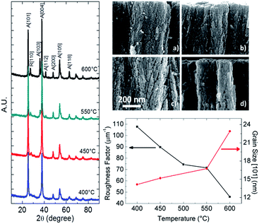 |
| | Fig. 1 (Left) XRD spectra of TiO2 film fabricated by PLD and annealed for 2 hours at different temperatures (top right) SEM images of the same samples annealed at (a) 400 °C, (b) 450 °C, (c) 500 °C and (d) 600 °C. (Bottom right) Roughness factor (black) for TiO2 samples annealed different annealing temperatures measured with colorimetric technique of the desorbed dye (N719) and crystal grain size (red) measured on the (101) peak by means of Scherrer equation. | |
Dye sensitized solar cells performances
In order to correlate the crystalline domain size and roughness factor with the DSC performances, devices were fabricated with a 5 μm TiO2 thick photoanodes using C106 (see ref. 28 for the dye chemical structure) dye and an iodide/triiodide redox electrolyte. While PLD deposition parameters are kept constant, by varying the annealing temperature, an optimum between crystalline domain size and roughness factor is found at 450 °C. As shown in Table 1, the overall efficiency is decreased by the predominant effect of the photocurrent density (J) which decreases from 15.7 (annealing at 450 °C) to 14.0 mA cm−2 (annealing at 600 °C) (Fig. 2). The trend can be related to the lower dye uptake due to a decrease in surface area caused by the suppression of inter-grain interfaces and by the increase in grain size. The samples annealed at 400 °C show lower short circuit current density (Jsc) compared to the samples annealed at 450 °C. This is in contrast with the trend found over the other annealing temperatures and it is attributed to scarce crystallinity of the samples.
Table 1 Photovoltaic parameters of DSC made with 5 μm thick nanotrees TiO2 photoanode annealed for 2 hours at different temperatures
| Samples |
Voc (V) |
Jsc (mA cm−2) |
FF |
PCE (%) |
| h-PA 400 °C |
0.712 |
14.6 |
0.72 |
7.6 |
| h-PA 450 °C |
0.737 |
15.7 |
0.75 |
8.7 |
| h-PA 500 °C |
0.746 |
14.9 |
0.74 |
8.3 |
| h-PA 550 °C |
0.749 |
15.0 |
0.73 |
8.3 |
| h-PA 600 °C |
0.763 |
14.0 |
0.74 |
7.9 |
| PA |
0.724 |
12.5 |
0.72 |
6.7 |
 |
| | Fig. 2 Effect of the annealing temperature of the photoanode on the IV characteristic for DSSC devices. The film thickness is 5 μm. | |
The open circuit voltage (Voc) follows an opposite trend possibly thanks to a reduce number of defects within the crystalline domains. The Voc of the samples annealed at 400 °C is approximately 50 mV lower compared to those with larger crystals annealed at 600 °C. The different surface areas available may also contribute to the Voc trend because of the different amount of dye molecules adsorbed on the surface. It is worth noticing that all devices based on hyperbranched nanostructures (red and blue lines) improves photovoltaic performances of reference devices (black line) comprising mesoporous layer in the same dye/electrolyte environment.
The reason behind the performance improvement shown by devices based on hyperbranched photoanode (h-PA) is two-fold. Optimized hyperbranced nanostructures, as reported in Fig. 3 show faster charge transport in comparison to standard mesoporous photoanode. The transport time constant for hyperbranched and control PA were measured by small photocurrent transient and are compared at the same charge density at short circuit current in the film. The electronic transport in h-PA TiO2 is 3 to 5 times faster than in PA depending on the charge at Jsc. The higher incident photon to current efficiency (IPCE) reflects the increase in Jsc. In the spectral region where the dye molar absorptivity is lower, the dye uptake level determines IPCE broadness. This is also evinced by the fact that, in the 600–700 nm region, IPCE of the h-PA annealed at 600 °C (lowest surface area) is lower than the one of h-PA annealed at 450 °C (high surface area). Typical thickness of the mesoporous photoanode used for high efficiency DSSC in conjunction with ruthenium dyes and iodide/triiodide redox couple is generally in the range of 15 μm.31 Indeed, in order to increase the light harvesting efficiency (LHE), and thus the IPCE, of the device in those regions of the light spectrum where the molar absorptivity of the dye is low,32 normally the PA is made as thick as allowed by electron diffusion length of the mesoporous layer and a scattering overlayer comprising hundreds of nanometers large nanoparticles is added as to exploit light scattering and enhance the PA optical thickness. In the case of h-PA, the quasi 1D nanostructures, presenting an inverse-conical envelope with their lateral dimension increasing as the film grows thicker, work as an integrated broadband scattering element.26 As the optical analysis reveals, beside the increase in light harvesting efficiency (LHE), given by the higher dye uptake of thicker h-PA, the films display an intense and broad light scattering as shown in Fig. 4 (bottom) by the haze factor (i.e. diffuse over total transmittance ratio). As the film grows thicker the LHE saturates until 600 nm while the haze factor (i.e. the ratio between diffused and total transmittance) gets closer to unity throughout the whole visible spectrum. Most importantly, to verify whether an increase in thickness could give rise to a significant increase in PCE, we tested devices with h-PA as thick as 5, 10 and 15 μm (Table 2). JV curves and the IPCE spectra are reported in Fig. 5. A broadening of 30 nm in the red-region is observed in the IPCE spectra as expected from the optical analysis. The current densities of the 5, 10 and 15 μm thick photoanodes measured under solar simulator at 0.1 sun condition are 1.52, 1.68 and 1.72 mA cm−2 whilst at full sun (98.8%) 14.6, 16.4 and 16.6 mA cm−2. The Jsc measured with solar simulator, is compared to the one calculated by multiplying the electron charge by the integral of the IPCE spectrum times the solar simulator lamp spectrum over the visible range (340–800 nm). The calculated current density for the 5, 10 and 15 μm is 14.6, 16.1, 17.4 mA cm−2, respectively. The relative increment in the current density between the 5 μm thick film and 10 μm thick film is in good agreement for all the three measurements being 10%, 10% and 12% for IPCE calculation, the 0.1 sun and 1 sun measurements, respectively. When passing from 10 μm to 15 μm the relative gain of the current is lower. For the full sun measurement only 1.2% of relative increment is measured in contrast to the 2.4% of 0.1 sun and the 8% of the IPCE measurement.
 |
| | Fig. 3 Transient and charge extraction measurements. | |
 |
| | Fig. 4 (Left) Light Harvesting Efficiency spectra (LHE) of films of different thicknesses loaded with a ruthenic dye and showing both increasing absorption intensity and spectral broadening. (Right) Haze factor of h-PA of different thicknesses. | |
Table 2 Photovoltaics performances for samples with different thicknesses
| h-PA thickness (μm) |
Voc (V) |
Jsc (mA cm−2) |
FF |
PCE (%) |
| 5 |
0.724 |
14.6 |
0.76 |
8.1 |
| 10 |
0.712 |
16.4 |
0.74 |
8.8 |
| 15 |
0.692 |
16.6 |
0.72 |
8.4 |
 |
| | Fig. 5 Nanotree TiO2 film with various thicknesses (5, 10, 15 μm) in conjunction with a volatile solvent based iodine electrolyte (Dye C106). The Voc of the devices decreased and the Jsc increased up to 15 μm of the TiO2 film. IPCE graph of DSC made with C106 and photoanode thickness of 5, 10 and 15 μm. The densification of the film with increasing thickness is responsible for the saturation of the current observed. | |
We attribute the saturation of photovoltaic performance of the device with h-PA (15 μm thick) to a morphological modification occurring at the top part of hyperbranched nanostructures above a certain thickness. As already stated, the hyperbranched nanostructures present an inverse-cone like outline with a top part size increasing with thickness. As the film grows thicker a densification phenomenon occurs on the top part of the film of the hyperbranched nanostructures, and the roughness factor (RF, i.e. the effective surface area over the geometric surface area of the samples), does not increase linearly with film thickness. In Fig. 6 the RF values versus film thicknesses are plotted. They represent average surface area estimations along the whole film thickness and thus the terminal part of each film must possess much lower (and always decreasing) roughness factor with respect to those plotted. The enlargement of the heads of the inverse-cone structures is at the same time increasing the scattering, as proven by the increased haze factor in Fig. 5, but with thickness it is also progressively lowering the dye uptake capability of the nanostructures. Further process optimization is required in order to improve the control on film morphology along its thickness and to enhance light harvesting. Additionally, the lower porosity of the top part of the layer, obstacles the iodide/triiodide redox shuttle diffusion and its capability to percolate into the mesoporous structure. The latter phenomenon is also testified by current dynamics reported in the ESI.† The best efficiency in the system comprising C106 dye and iodide/triiodide electrolyte was obtained with the 10 μm film mainly because the higher Voc with respect to the 15 μm. In a parallel experiment, we compared a 17 μm thick h-PA device with a 17 μm standard device with scattering layer (12 μm mesoporous layer + 5 μm of scattering overlayer) obtaining similar power conversion efficiencies (9.23% vs. 9.21% respectively). h-PA were successfully tested also with a cobalt electrolyte in a similar configuration as in ref. 33 obtaining an overall efficiency of about 10% at 1 sun illumination.
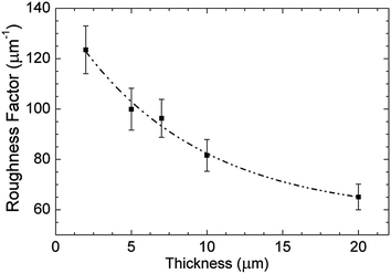 |
| | Fig. 6 Roughness factor per micron at a given thickness in h-PA. | |
Conclusions
The influence on photovoltaic performances of different crystalline domain size and dye loadings has been investigated for hyperbranched quasi 1D nanostructures. An optimum compromise between crystallinity (grain size [101] ≈ 15 nm) and surface area (RF ≈ 90) was found confirming the fact that large crystalline domains must be accompanied by surface roughness offering anchoring sites for dye molecules. Rather than the open circuit voltage caused by larger crystalline domains, it was shown that the higher photocurrent density induced by higher dye uptake is the characteristic mostly affecting the power conversion efficiency of h-PA dye sensitized solar cells. Eventually an optimized nanostructure was compared to a standard mesoporous photoanode. The array of hyperbranched nanostructures was found to enhance photogenerated current (+25%) thanks to intense light diffusion enhancing the photoanode optical thickness. In 5 μm thick films, the elongated structures together with the anisotropic and directional crystal growth contributed to improve electron transport and thus photovoltaic performance of nearly +30%. Despite higher current was found for thicker h-PA the increase in performance was limited by a densification of the top part of the film. This was thought to lead to scarce dye loading increase and to a worsened mass transport.
Experimental
Pulsed laser deposition
Hyperbranched nanostructures are deposited by pulsed laser deposition (PLD). In PLD a KrF excimer laser (λ = 248 nm, 20 ns) with 400 mJ energy per pulse and fluence of ∼2.5 J cm−2 operating at 20 Hz ablates a target of TiO2 (purity of 99.99%, Testbourne). Hence a nanoparticles inseminated plasma plume that expands normally to the target surface and condensate on the sample placed face-on to the target. As the whole process is occurring in a vacuum chamber, it is possible to control the kinetic of clusters formation by varying the background pressure. In this work samples are fabricated in an atmosphere of 7 Pa in oxygen.
Dye sensitized solar cells fabrication
The photoanode consists of thin TiO2 electrodes comprising a 5 μm mesoporous TiO2 layer (18 nr T Dyesol, particle size, 18 nm) on a TEC7. The layer was sintered and subsequently soaked 30 minutes at 70 °C in a 40 mM TiCl4 deionized water solution and heated again at 500 °C for only 15 minutes prior sensitization. The complete working electrode was prepared by immersing the film into the dye solution (0.1 mM of C106 in acetonitrile/tert-butanol mixture plus 0.4 mM of DINHOP) for 3 h. A fluorine-doped tin oxide (FTO) glass counter electrode was platinized and then sealed together with the working electrode using a 25 μm thick hot melt film (Surlyn, Dupont) by heating the system at 100 °C. Devices were filled with the electrolyte coded Z960 through holes previously drilled in the counter electrodes. Finally the holes were sealed with a Surlyn sheet and a thin glass cover by heating again a 100 °C.
Solar simulator and external quantum efficiency measurements
The current–voltage curve was acquired using a light source comprising a 450 W xenon lamp (Oriel, USA). A Schott K113 Tempax sunlight filter (Präzisions Glas & Optik GmbH, Germany) was used to reduce the mismatch between the simulated and actual solar spectrum to less than 2%. For data acquisition a Keithley model 2400 digital source meter (Keithley, USA) was used. The photoactive area of was defined by a black mask of 6 × 6 mm2 was used to limit the photoactive area to 0.16 cm2. Incident photon-to-current conversion efficiency measurements were from the monochromated visible photons, from Gemini-180 double monochromator Jobin Yvon Ltd. (UK), powered by a 300 W xenon light source (ILC Technology, USA) superimposed on a 10 mW cm−2 LED light. The monochromatic incident light was passed through a chopper running at 1.8 Hz frequency.
Photocurrent and photovoltage decay measurements
For the transient photovoltage/photocurrent decay measurements, a white light bias was generated from an array of diodes. Red light pulse diodes (with a square pulse width, 100 ns rise and fall time) controlled by a fast solid state switch were used as the perturbation source. The voltage dynamics were recorded on a PC interfaced Keithley 2602 source meter with a 500 μs response time. The perturbation light source was set to a suitably low level in order to assume the system to be linear. By varying the white light bias intensity, the electron recombination lifetime could be estimated over a range of applied biases. Before the LEDs switched to the next light intensity, a charge extraction routine was executed to measure the electron density in the film. In the charge extraction techniques, the LED illumination source was turned off in <1 μs, while simultaneously, the cell was switched from open to short circuit. The resulting current, as the cell returns to V = 0 and J = 0, was integrated to give a direct measurement of the excess charge in the film at that Voc.
XRD measurement
X-ray powder diffraction experiments were carried out on a Bruker D8 Advance diffractometer operating in reflection mode with Ge-monochromated Cu Kα1 radiation (λ = 1.5406 Å) and a linear position-sensitive detector; with a 2θ range 20–80° and a step size 0.016°.
Roughness factor measurements
UV/vis spectrophotometer was used for the chromatographic measurement for roughness factor evaluation. After 27 hours of 0.2 mM N719 dye loading, dye is desorbed from the photoanodes with a known amount of 0.1 M of NaOH in water. The concentration of the desorbed dye solution is defined though measuring the absorption spectra of the solution by UV/VIS spectroscopy; desorbed dye molecules number is estimated. Knowing the area of a dye molecule (1.6 nm2) it is possible to retrieve the roughness factor of the photoanode.
Optical characterization
All optical measurements are performed with a UV/vis spectrophotometer equipped with an integrating sphere (Perkin-Elmer Lambda 1050 spectrophotometer Xe lamp).
Acknowledgements
F.D.F. acknowledge funding from “Photovoltaic Building Integrated Glass Tiles for Innovative Architectural Application” (TIFAIN), MIUR Regione Lombardia ID number 30221157.
Notes and references
- N. Tetreault and M. Gratzel, Energy Environ. Sci., 2012, 5, 8506–8516 CAS.
- L.-P. Heiniger, F. Giordano, T. Moehl and M. Grätzel, Adv. Energy Mater., 2014, 4, 201400168 Search PubMed.
- A. Mihi and H. Miguez, J. Phys. Chem. B, 2005, 109, 15968–15976 CrossRef CAS PubMed.
- M. E. Calvo, S. Colodrero, T. C. Rojas, J. A. Anta, M. Ocaña and H. Míguez, Adv. Funct. Mater., 2008, 18, 2708–2715 CrossRef CAS.
- T. G. Deepak, G. S. Anjusree, S. Thomas, T. A. Arun, S. V. Nair and A. Sreekumaran Nair, RSC Adv., 2014, 4, 17615–17638 RSC.
- Y.-C. Park, Y.-J. Chang, B.-G. Kum, E.-H. Kong, J. Y. Son, Y. S. Kwon, T. Park and H. M. Jang, J. Mater. Chem., 2011, 21, 9582–9586 RSC.
- H.-J. Koo, J. Park, B. Yoo, K. Yoo, K. Kim and N.-G. Park, Inorg. Chim. Acta, 2008, 361, 677–683 CrossRef CAS.
- S. Hore, C. Vetter, R. Kern, H. Smit and A. Hinsch, Sol. Energy Mater. Sol. Cells, 2006, 90, 1176–1188 CrossRef CAS.
- S. Mathew, A. Yella, P. Gao, R. Humphry-Baker, F. E. CurchodBasile, N. Ashari-Astani, I. Tavernelli, U. Rothlisberger, K. NazeeruddinMd and M. Grätzel, Nat. Chem., 2014, 6, 242–247 CrossRef CAS PubMed.
- J.-H. Yum, T. W. Holcombe, Y. Kim, K. Rakstys, T. Moehl, J. Teuscher, J. H. Delcamp, M. K. Nazeeruddin and M. Grätzel, Sci. Rep., 2013, 3, 2446 Search PubMed.
- A. Yella, H.-W. Lee, H. N. Tsao, C. Yi, A. K. Chandiran, M. K. Nazeeruddin, E. W.-G. Diau, C.-Y. Yeh, S. M. Zakeeruddin and M. Grätzel, Science, 2011, 334, 629–634 CrossRef CAS PubMed.
- J. Villanueva-Cab, S.-R. Jang, A. F. Halverson, K. Zhu and A. J. Frank, Nano Lett., 2014, 14, 2305–2309 CrossRef CAS PubMed.
- K. Zhu, N. R. Neale, A. Miedaner and A. J. Frank, Nano Lett., 2006, 7, 69–74 CrossRef PubMed.
- M. Law, L. E. Greene, J. C. Johnson, R. Saykally and P. Yang, Nat. Mater., 2005, 4, 455–459 CrossRef CAS PubMed.
- F. Sauvage, F. Di Fonzo, A. Li Bassi, C. S. Casari, V. Russo, G. Divitini, C. Ducati, C. E. Bottani, P. Comte and M. Graetzel, Nano Lett., 2010, 10, 2562–2567 CrossRef CAS PubMed.
- C. Dong, W. Xiang, F. Huang, D. Fu, W. Huang, U. Bach, Y.-B. Cheng, X. Li and L. Spiccia, Nanoscale, 2014, 6, 3704–3711 RSC.
- X. Sheng, D. He, J. Yang, K. Zhu and X. Feng, Nano Lett., 2014, 14, 1848–1852 CrossRef CAS PubMed.
- M. Ye, X. Xin, C. Lin and Z. Lin, Nano Lett., 2011, 11, 3214–3220 CrossRef CAS PubMed.
- M. McCune, W. Zhang and Y. Deng, Nano Lett., 2012, 12, 3656–3662 CrossRef CAS PubMed.
- L. De Marco, M. Manca, R. Giannuzzi, M. R. Belviso, P. D. Cozzoli and G. Gigli, Energy Environ. Sci., 2013, 6, 1791–1795 CAS.
- H. Yao, J. Ma, Y. Mu, Y. Chen, S. Su, P. Lv, X. Zhang, D. Ding, W. Fu and H. Yang, RSC Adv., 2015, 5, 6429–6436 RSC.
- Y. M. Liu, M. L. Zhang, Y. Jiang, Y. Xia, W. W. Sun and X. Z. Zhao, Electrochim. Acta, 2015, 173, 483–489 CrossRef CAS.
- W.-Q. Wu, Y.-F. Xu, H.-S. Rao, C.-Y. Su and D.-B. Kuang, J. Am. Chem. Soc., 2014, 136, 6437–6445 CrossRef CAS PubMed.
- W.-Q. Wu, Y.-F. Xu, H.-S. Rao, C.-Y. Su and D.-B. Kuang, J. Phys. Chem. C, 2014, 118, 16426–16432 CAS.
- W. Q. Wu, H. L. Feng, H. S. Rao, Y. F. Xu, D. B. Kuang and C. Y. Su, Nat. Commun., 2014, 5, 3968 CAS.
- L. Passoni, F. Ghods, P. Docampo, A. Abrusci, J. Martí-Rujas, M. Ghidelli, G. Divitini, C. Ducati, M. Binda, S. Guarnera, A. Li Bassi, C. S. Casari, H. J. Snaith, A. Petrozza and F. Di Fonzo, ACS Nano, 2013, 7, 10023–10031 CrossRef CAS PubMed.
- L. S. Hsu, R. Rujkorakarn, J. R. Sites and C. Y. She, J. Appl. Phys., 1986, 59, 3475–3480 CrossRef CAS.
- R. Buonsanti, E. Carlino, C. Giannini, D. Altamura, L. de Marco, R. Giannuzzi, M. Manca, G. Gigli and P. D. Cozzoli, J. Am. Chem. Soc., 2011, 133, 19216–19239 CrossRef CAS PubMed.
- Y.-w. Jun, M. F. Casula, J.-H. Sim, S. Y. Kim, J. Cheon and A. P. Alivisatos, J. Am. Chem. Soc., 2003, 125, 15981–15985 CrossRef CAS PubMed.
- J. Liang, G. Zhang, J. Yang, W. Sun and M. Shi, AIP Adv., 2015, 5, 017141 CrossRef.
- Y. Cao, Y. Bai, Q. Yu, Y. Cheng, S. Liu, D. Shi, F. Gao and P. Wang, J. Phys. Chem. C, 2009, 113, 6290–6297 CAS.
- J. Lin, Y.-U. Heo, A. Nattestad, M. Shahabuddin, Y. Yamauchi and J. H. Kim, Phys. Chem. Chem. Phys., 2015, 17, 7208–7213 RSC.
- A. Yella, H. W. Lee, H. N. Tsao, C. Y. Yi and A. K. Chandiran, Science, 2011, 334, 629–634 CrossRef CAS PubMed.
Footnotes |
| † Electronic supplementary information (ESI) available. See DOI: 10.1039/c5ra19542j |
| ‡ These authors equally contributed to the work. |
|
| This journal is © The Royal Society of Chemistry 2015 |
Click here to see how this site uses Cookies. View our privacy policy here. 


