DOI:
10.1039/C5RA19300A
(Paper)
RSC Adv., 2015,
5, 102318-102322
Physical model of threshold switching in NbO2 based memristors
Received
18th September 2015
, Accepted 20th November 2015
First published on 24th November 2015
Abstract
This paper investigates the origin of the threshold switching effect in NbO2. It is found that the effect is independent of the metal-insulator-transition but can be explained by a trap-assisted Frenkel–Poole like conduction mechanism in combination with a moderate temperature increase by only 150 K due to Joule heating. These findings lead to the development of a physics based model which is of pure electrical nature and explains the occurrence of the threshold effect as well as the negative-differential resistance behavior observed in NbO2.
Introduction
Threshold switching effects in filamentary switching memristors based on niobium oxide have attracted increasing attention due to their potential to realize scalable selector devices for resistive random access memories (ReRAM).1–4 Moreover, the negative differential resistance (NDR) region in the quasi-static current–voltage characteristic, underlying the threshold switching effect, supports the occurrence of local activity, giving rise to the appearance of sustained oscillations in a parallel connection of a capacitor with the memristor.5,6 Finally, the threshold switching device based implementation of the neuristor circuit is able to exhibit various biomimetic properties pertaining to a biological axon membrane and enables computational universality.7,8 A widely accepted physical model for the threshold switching effect based on a metal-insulator-transition (MIT) in a NbO2 based nano-structure was proposed in 2012. It assumes a cylindrical conducting filament composed of two phases. While the inner part of the filament consists of a metallic phase with high conductivity, the surrounding outer part has an oxidic phase with low conductivity.9 The high current density in the inner filament increases the internal temperature due to Joule heating. Exceeding the MIT transition temperature of about 1070 K, a fraction of the outer filament turns into the metallic phase, thus reducing the overall resistance of the device. Hence, the overall resistance value depends on the metallic phase fraction u, which is the internal state variable of the model. The proposed model describes the threshold switching effect fairly well when looking on a linear plot of the quasi-static current–voltage (im–vm) characteristic. However, comparing the logarithmic im–vm characteristic below the threshold voltage uncovers deviations between model and measurements. Thus, the ohmic conduction mechanism of the geometric model cannot satisfactorily capture the electrical behavior of the device. Another electric field induced model describes the threshold switching in amorphous chalcogenide glasses by a Frenkel–Poole conduction mechanism.10 It assumes a non-equilibrium population of shallow traps at high electric fields and a resulting substantial non-uniformity of electric field in the amorphous layer, but neglects all thermal effects related to Joule heating in the non-filamentary device. However, the results of a temperature dependent characterization of our NbO2 based devices led to the extraction of the internal temperature of the conducting filament which was found to be in the range of 550 K. This value is comparable to the filament internal temperature which was estimated for other filamentary switches, such as the TaO2-based device,11 but which is much lower than the typical MIT-transition temperature of NbO2. These facts indicate that another threshold switching model is mandatory to describe the complete electrical characteristic.
Experimental
Our memristors with a pad diameter of 50 μm consist of a Nb2O5/NbOx oxide stack sandwiched between two platinum electrodes. The detailed fabrication process is described elsewhere.2 Electrical measurements were performed by a Keithley 4200 SCS. Before measurement a conducting filament was created in a forming step by applying a voltage ramp from 0 to −4 V in 10 mV steps with an applied current compliance of ICC = 7 mA. While the Nb2O5 single layer in a Pt/Nb2O5/Pt MIM-structure behaves like a dielectric, the sub-stoichiometric NbOx layer exhibits high conductivity when sandwiched as a thin single layer in between two Pt-electrodes and no electroforming of a filament is possible. That is, the resistance state in the double layer MIM-structure Pt/Nb2O5/NbOx/Pt is mainly determined by the filaments electronic structure which is formed in the stoichiometric Nb2O5 portion of the double layer.
Results and discussion
Memristor characteristic
Fig. 1(a) shows the im–vm characteristic of the memristor in negative voltage polarity for ambient temperatures Tamb ranging from 243 K to 380 K. During the measurement the voltage was directly forced to the device in a quasi-static voltage sweep, while a current compliance limits the current at ICC = 7 mA to prevent changes in filaments atomic structure. Since the device characteristic is mainly defined by the filament, the im–vm characteristic is nearly symmetric and gives similar results in positive voltage polarity. At low voltages (vm = 0 to −0.6 V) the current increases exponentially until a strong kink in the im–vm characteristic occurs which increases the current level by two orders of magnitude. However, the effect is volatile. After decreasing the voltage again, the current jumps back to the original level. Thereby, the jump back occurs at several hundred millivolts less resulting in a hysteresis. With increasing ambient temperature Tamb the current level at low voltages (vm = 0 to −0.6 V) increases. From the Arrhenius plot (Fig. 1(c)) we extrapolated an activation energy of Ea = 0.215 V at vm = −0.5 V. The onset of the threshold effect Vth is also temperature dependent.12 At higher ambient temperature the onset shifts from Vth = −1.1 V to Vth = −0.6 V while the hysteresis and the kink is less pronounced. When plotting Vth over the ambient temperature, a linear trend can be seen (Fig. 1(b)). Extrapolating towards a threshold voltage of 0 V yields a temperature of about 550 K. Even though a different physical effect might affect the linear trend at higher temperatures, the results indicate that the transition into the low-resistance state could occur already at 0 V for an increased ambient temperature of 550 K. Although the metal-insulator transition effect – which occurs at 1070 K in NbO2 – can't be ruled out, that finding clearly points to another mechanism as dominant effect leading to the threshold switching behavior at much lower temperatures.
 |
| | Fig. 1 (a) Quasi-static current–voltage characteristic measured at different temperatures. A current compliance limits the current at ICC = 7 mA to prevent changes in resistance state of the device. (b) Ambient temperature dependence of the threshold voltage Vth extracted from the current–voltage characteristic of plot (a). (c) Arrhenius plot of the measured current im (symbols), extracted at a voltage of vm = −0.5 V and Arrhenius fit according to im ∼ exp(Eak−1Tamb−1) with Ea = 0.215 eV. | |
The steep current increase at the threshold voltage results from the direct application of the voltage across the memristor device.5 To stabilize the measurement and to get a continuous im–vm curve a series resistor Rser can be inserted between the voltage source and the memristor (inset in Fig. 2). At low voltages the resistance of the memristor is much higher than the series resistor thus most of the voltage drops over the memristor. If threshold voltage is reached, the resistance of the memristor decreases and the increasing current leads to a significant voltage drop over the series resistor. Thus memristor and series resistor build a voltage divider, stabilizing the negative differential resistance region of the memristor device. In comparison to the setup without a resistor this configuration allows to increase the current in small steps avoiding current jumps. Fig. 2 compares the measured device characteristic for the two cases with and without a connected series resistor Rser. Note, that in both cases a quasi-static voltage sweep was applied. Obviously, a very smooth transition between the pre-threshold region and the post-threshold region is obtained, and the hysteresis vanishes. Instead, a NDR region becomes visible. That means, that the starting point of the NDR region and its curvature define the hysteresis in the circuit without additional resistor. The current compliance is typically realized by reducing the applied voltage over the device to limit the current flow to the maximal allowed value. Hence, without the stabilizing resistor, when the threshold voltage is reached (point A in Fig. 2), the current jumps towards the current compliance value and voltage is reduced accordingly, thus reaching point B, even though the parameter analyzer displays the pre-defined voltage value. If the voltage is decreased again, the current jumps back once the applied voltage escapes the NDR-region (left from point B in Fig. 2). The smooth transition between sub-threshold region and NDR-region indicates the physical phenomenon in both regions might be similar and based on a thermally activated conduction process where the MIT of the NbO2 is not the dominant mechanism.
 |
| | Fig. 2 Quasi-static im–vm characteristic of the threshold switching device with and without a stabilizing resistor of value Rser = 330 Ω. The inset shows the measurement circuit with series resistor. | |
Threshold switching model
Based on the results reported above a model for the threshold switching effect is developed. The model describes the conduction mechanism which dominates the current flow below threshold voltage as well as the self-heating of the filament at higher currents. To model the conduction process the temperature dependent characteristic of Fig. 1(a) below threshold was tested for different mechanisms like Fowler–Nordheim tunneling, trap assisted tunneling, Schottky emission and Frenkel–Poole conduction.13 The best agreement was found for Frenkel–Poole conduction, as shown in the Frenkel–Poole plot for two different ambient temperatures (Fig. 3). Clearly visible is the linear region below the threshold. Even thought, there are slight deviations from the expected behavior of an ideal Frenkel–Poole mechanism, the modeled IV-characteristic below threshold shows reasonable agreement with the measurement data as depicted in Fig. 4(a). From the Frenkel–Poole equation one can derive the device resistance expression as| |
 | (1) |
where R0 is a constant, Ea the activation energy describing the energetic trap level below the conduction band, q the elementary charge, E = vm/tox is the electrical field, ε0 the vacuum permittivity, εr the relative permittivity, k the Boltzmann constant and Tm the internal temperature of the filament.
 |
| | Fig. 3 Frenkel–Poole plot (ln(im/Em) vs. Em0.5) for curves at two different ambient temperatures Tamb = 25 °C and 70 °C. The dotted straight lines are mean square fits to the linear region of the curves indicating Frenkel–Poole conduction below threshold voltage. | |
 |
| | Fig. 4 (a) Comparison between measured quasi-static im–vm characteristic (symbols) and modeled im–vm characteristic according to eqn (1)–(3) (lines). A current compliance of 2 mA was enforced. (b) Model-based plot of the filament internal temperature Tm over the current im flowing through the memristor. In both plots curves are shown at two different ambient temperatures Tamb = 25 °C and 70 °C. Table 1 summarizes the model parameter. | |
For the description of the self-heating effect we assume all the current flows through the filament leading to a temperature increase by Joule heating. On the other side the filament releases heat to the environment. This leads to the following differential equation with the temperature Tm denoting the state variable:
| |
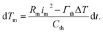 | (2) |
The first term in eqn (2) describes the temperature increase due to Joule heating, where Rm is the device resistance depending on the filament internal temperature Tm and the activation energy Ea according to eqn (1). im denotes the current through the memristor's filament, and Cth is the thermal capacitance. The second term describes the temperature reduction in the filament due to heat transfer in the oxide film as well as towards the electrodes, characterized by the thermal conductance Γth and the temperature difference ΔT = Tm − Tamb between ambient temperature Tamb and filament internal temperature Tm. Since the switching effect is volatile, diameter and length of the filament are treated as constants and are defined by the initial forming step. The heat capacitance Cth as well as the thermal conductance Γth of the filament are both temperature dependent. However, in the temperature range of interest their relative change is only moderate compared to the temperature dependence of other terms. Consequently, in a first-order approximation these physical quantities can be treated as constants as well. In the quasi-static case applies Rmi2m = ΓthΔT, and hence Cth has no influence on the shape of the quasi-static im–vm characteristic.
Ohm's law describes the relation between the applied voltage v, the voltage drop over the memristor vm and the current im, where Rser is a resistor connected in series to the device.
| | |
v = (Rm + Rsec)im = vm + Rsecim
| (3) |
Fig. 4(a) demonstrates a very good agreement between measurement and numerical calculation based on eqn (1)–(3) at two exemplary ambient temperatures. For the calculations we also assumed quasi-static conditions (t → ∞). Obviously, the model fits the data below as well as in the NDR region above the threshold. Table 1 summarizes the corresponding model parameters. The temperature dependence at currents below 0.05 mA of the device resistance is well described by the activation energy Ea. In addition, the model describes the change of the curvature in the NDR region at different temperatures. At higher temperatures the curvature becomes less pronounced. Since the curvature defines the hysteresis in the circuit without additional resistor, the model behavior is in good agreement with Fig. 1(a) where the hysteresis vanishes with increasing temperature. Fig. 4(b) plots the modeled filament internal temperature Tm over the device current which follows Tm = Tamb + Rmim2/Γth in steady state. Γth critically affects the modeled internal temperature and was carefully chosen to match the im–vm characteristic. At small currents well below 0.05 mA the temperature change due to Joule heating is very small and the filament internal temperature is close to ambient temperature. However, with increasing current the temperature rises, leading to a decrease in device resistance. Already a moderate increase in filament internal temperature (by just 150 K) can result in a significant reduction in device resistance, inducing the NDR based threshold switching effect. Although an underestimated Γth would lead to a much faster increase of Tm, the Frenkel–Poole induced threshold switching effect would still occur far below the MIT temperature of 1070 K, indicating that the MIT is not the dominant mechanism behind the threshold switching effect.
Table 1 Model parameters for the im–vm characteristic depicted in Fig. 4(a)
| Physical quantity |
Symbol |
Value |
Unit |
| Thermal capacitance |
Cth |
5.0 × 10⁻¹⁰ |
J K−1 |
| Thermal conductance |
Γth |
5.7 × 10⁻⁶ |
W K−1 |
| Series resistor |
Rser |
330 |
Ω |
| Bolzmann's constant |
k |
1.38 × 10⁻²³ |
J K−1 |
| Activation energy |
Ea |
0.215 |
eV |
| Electron charge |
q |
1.60 × 10⁻¹⁹ |
C |
| Fitting constant |
R0 |
34.0 |
Ω |
| Vacuum permittivity |
ε0 |
8.85 × 10⁻¹² |
F m−1 |
| Relative permittivity |
εr |
45 |
|
| Oxide thickness |
tox |
18 |
nm |
Conclusions
In this paper we developed a physical model, which describes the threshold switching effect in NbO2 based filamentary switching devices by a temperature activated Frenkel–Poole conduction mechanism. The threshold switching effect is disclosed to be of pure electronic nature in combination with a moderate temperature increase due to Joule heating in the range of 150 K. That is, the threshold switching effect occurs well below the onset of MIT in NbO2. Since our model is independent of material specific properties like the MIT effect, it might be adapted to explain the threshold switching effects which were observed in filamentary switching devices based on other transition metal oxides (i.e. Ta2O5, HfO2, TiO2 or oxides based on Mo and W).14,15
Acknowledgements
The authors acknowledge the Initiative and Network Fund of German Helmholtz Association, Helmholtz Virtual Institute VH-VI-442 MEMRIOX and the contribution and networking support of the EU COST Action IC1401.
References
- X. Liu, S. Md. Sadaf, M. Son, J. Park, J. Shin, W. Lee, K. Seo, D. Lee and H. Hwang, IEEE Electron Device Lett., 2012, 33, 236 CrossRef CAS.
- H. Mähne, H. Wylezich, S. Slesazeck, T. Mikolajick, J. Vesely, V. Klemm and D. Rafaja, IEEE International Memory Workshop (IMW), 2013, p. 174 Search PubMed.
- E. Cha, J. Woo, D. Lee, S. Lee, J. Song, Y. Koo, J. Lee, C. G. Park, M. Y. Yang; K. Kamiya, K. Shiraishi, B. Magyari-Kope, Y. Nishi and H. Hwang, IEDM, 2013, p. 268 Search PubMed.
- S. K. Nandi, X. Liu, D. K. Venkatachalam and R. G. Elliman, J. Phys. D: Appl. Phys., 2015, 48, 195105 CrossRef.
- A. Ascoli, S. Slesazeck, H. Mähne, R. Tetzlaff and T. Mikolajick, IEEE Transactions on Circuits and Systems I: Regular Papers, 2015, 62, 1165 CrossRef.
- S. Li, X. Liu, S. K. Nandi, D. K. Venkatachalam and R. G. Elliman, Appl. Phys. Lett., 2015, 106, 212902 CrossRef.
- M. D. Pickett, G. Medeiros-Ribeiro and R. S. Williams, Nat. Mater., 2013, 12, 114 CrossRef CAS PubMed.
- M. D. Pickett and R. S. Williams, Nanotechnology, 2013, 24, 384002 CrossRef PubMed.
- M. D. Pickett and R. S. Williams, Nanotechnology, 2012, 23, 215202 CrossRef PubMed.
- D. Ielmini and Y. Zhang, J. Appl. Phys., 2007, 102, 054517 CrossRef.
- Y. Nishi, S. Menzel, K. Fleck, U. Böttger and R. Waser, IEEE Electron Device Lett., 2014, 35, 259 CrossRef CAS.
- F.-C. Chiu, Adv. Mater. Sci. Eng., 2014, 2014, 578168 Search PubMed.
- S. Li, X. Liu, S. K. Nandi, D. Kumar Venkatachalam and R. G. Elliman, Optoelectronic and Microelectronic Materials & Devices (COMMAD), 2014, p. 138 Search PubMed.
- X. Saura, E. Miranda, D. Jiménez, S. Long, M. Liu, J. M. Rafí, F. Campabadal and J. Suné, Jpn. J. Appl. Phys., 2013, 52, 04CD06 CrossRef.
- V. P. Malinenko, A. L. Pergament, O. V. Spirin and V. I. Nikulshin, Journal on Selected Topics in Nano Electronics and Computing, 2014, 2, 45 Search PubMed.
|
| This journal is © The Royal Society of Chemistry 2015 |
Click here to see how this site uses Cookies. View our privacy policy here. 


