
Fabrication of a flexible copper pattern based on a sub-micro copper paste by a low temperature plasma technique†
Yue Gao,
Hao Zhang,
Jinting Jiu*,
Shijo Nagao,
Tohru Sugahara and
Katsuaki Suganuma
The Institute of Scientific and Industrial Research (ISIR), Osaka University, Mihogaoka 8-1, Ibaraki, Osaka 567-0047, Japan. E-mail: jiu@eco.sanken.osaka-u.ac.jp
First published on 8th October 2015
Abstract
Flexible devices have attracted much attention due to their great potential as next-generation electronics and for their applications in healthcare, fitness and AI robots. In these devices, the circuits composed of printed metal pastes are regarded as the key components on various flexible substrates. Although low temperature silver (Ag) paste has been applied in these devices, a high price and electromigration seriously limit their wide application. Copper (Cu), which has almost the same conductivity but is low cost and electromigration-resistant has been expected to be a substitute for the Ag-based paste. Herein, sub-micro copper particles with a suitable diameter were synthesized by a simple large-scale polyol method. A Cu paste was further formed from the Cu particles and printed onto a flexible substrate to form a Cu-based pattern. A reactive plasma process was used to sinter the copper pattern at low temperature. A high conductivity Cu pattern with a resistivity of 15.9 μΩ cm has been successfully fabricated with only 10 minutes sintering at 200 W due to an enhanced plasma effect. The temperature was below 75 °C during the plasma process. A V-shape Cu antenna pattern has also been arranged on PET to fabricate a flexible antenna device, and the results show that the pattern has the same sensitivity for high-frequency signals when compared to bulk commercial copper foil.
Introduction
Recently, a large scale roll-to-roll (R2R) industrial process based on solution paste1 has largely accelerated the development of printed electronics, which have attracted more and more interest for their potential applications in various electronic devices such as displays,2 transistors,3 sensors,4 electronic solar cell arrays,5 and radiofrequency identification (RFID) tags.6 In particular, due to the presence of smartwatches, market analysts believe that the global retail revenue from smart wearable devices will treble in 2016 and reach $53.2 billion in 2019, compared to $4.5 billion in 2015. In addition to the product design and sale, the quality of the product itself is a major factor in determining the market. As the key component of wearable devices, circuits have many functions and roles in these devices. Traditionally, bulk metal wires were used to connect every component. With the development of miniaturization and wearable devices fabricated by the rapid R2R process, printed metal pastes have become popular and powerful materials in these devices. Normally, these metal pastes, which are composed of metal particles, binder and solvent with a certain viscosity, are always coated or printed on the substrates. Then, the pastes are treated with heat energy to realize the conductivity and made into circuits in the devices.These days, silver pastes have been well studied due to excellent performance after sintering. Although a high temperature sintering process such as over 200 °C can make high conductivity circuits prepared from Ag pastes, the high temperature is extremely hazardous for most of the flexible substrates which are based on polymers and textiles (even paper). Therefore, various low temperature sintering methods, such as using microwave,7 flash light,8 and inert gas plasma,9,10 have been attempted to make high performance silver circuits. Cost-cutting is still an issue for the application of noble silver. Moreover, a short phenomenon due to the electromigration of silver-based circuits is also an inevitable problem, especially considering the microminiaturization trend of electronics products. In contrast, compared to silver, copper is only 6% less conductive but 1000 times more abundant and 100 times less expensive. More importantly, copper is also robust to electromigration. Therefore, copper paste has become a hot point and is considered a suitable alternative to silver paste these days.
Although copper has many advantages, it is susceptive to oxidation under ambient atmosphere. High temperature sintering under vacuum or reducing atmosphere are usually used to avoid oxidation.11–13 However, this process not only largely complicates the fabrication and increases the costs but it also limits the applications of most flexible substrates because the sintering temperature over 250 °C far exceeds the melt points of flexible substrates. Hence, the anti-oxidation method for copper pastes has been the burning question except for low-temperature sintering. Recently, some techniques, such as using a laser, intense light,14,15 etc., have been attempted to sinter copper nanoparticles in air and achieve high performance. In these processes, very small copper nanoparticles coated with a thick organic layer are utilized, and an extremely strong energy source has to be introduced to remove the organic layer and achieve the conductivity of the copper line with huge volume shrinkage. However, organic residues which would damage the devices in the last copper product were inevitable. Moreover, the preparation of very small copper nanoparticles not only increased the cost and difficulty but also initiated the rapid oxidization of small nanoparticles in the transport and storage steps. In order to mitigate the oxidization of copper nanoparticles and avoid the volume shrinkage, increasing the diameter of the particle to reduce the huge surface energy might be a suitable method. However, reducing surface energy also means there is a risk of reducing the sintering ability. Thus a corresponding effective sintering method is needed.
Plasma is an ionized gas consisting of approximately equal numbers of positively charged ions and negatively charged electrons. Due to its extremely active property, plasma has been proven to be very suitable for surface cleaning and chemical reaction. Although plasma has been used to prepare copper nanoparticles,16–18 the plasma sintering of copper particles is seldom reported. When compared to laser and intense light sintering,14,15 plasma sintering can use active species to firstly react and clean the surface of the copper particles, and then connect these net surfaces all together to achieve the annealing process. Moreover, these active plasma species also are expected to easily decompose the organic layer on the surface of the particles by chemical reaction which will largely decrease the sintering temperature. Based on the plasma sintering mechanism,19,20 not only nanoparticles but also sub even micro-particles with suitable diameter will undergo the process. Furthermore, compared to the normal plasma etching (PE) process, the reactive ion etching (RIE) process is expected to be a more effective method, which introduces a high-frequency electric field to accelerate the reaction between the active plasma species and copper particles.
In this study, sub-micro Cu particles were synthesized by a simple large-scale polyol method. The as-prepared Cu particles were made into a paste and printed on PET substrates by a simple printing method. The plasma process was applied to sinter the printed Cu pattern. An argon and hydrogen mixture was used as the feed gas to generate active species in the plasma process. The sintering parameters were observed, and a flexible antenna was designed to probe the return loss and performance based on these sintered Cu patterns. The result illuminates a promising route for the realization of flexible antennas that will be of great interest for a variety of applications, including wearable computers, flexible electronics, and healthcare sensors.
Experiment
Synthesis of copper paste
All reagents were purchased from Wako Pure Chemical Industries, Ltd. (Osaka, Japan) and were used without any further purification. 1.5 g polyvinyl pyrrolidone K90 (PVP) was used as a capping agent and dispersant, which was firstly dissolved into 1,3-propanediol (PPD), which was used as the solvent as well as reducing agent. Then 1.5 g copper hydroxide (Cu(OH)2), used as a copper source, also was dispersed in PPD following the addition of sodium sulfide (Na2S·5H2O) with a final concentration of 150 μM to control the morphology of the product. After that, the solution was put in a reactor under stirring at 190 °C for 90 min. With the general dissolution of the copper source, the color changed from blue to black and finally turned into bright red like bulk copper. Then the precipitates were washed with ethanol several times with centrifugation and kept in ethanol as a paste for further use. The paste was directly printed onto polyethylene terephthalate (PET) substrates by the doctor blade method with a size of 5 mm × 30 mm. After being dried in air at room temperature, all of the samples were sintered with a plasma process. The sintering temperature was detected by attaching a thermosensitive label on the back-side of the substrates. The plasma power and sintering time were clarified to look for optimized parameters. To make an antenna, the Cu paste was printed on the surface of PET with a V-shape. The length of the Cu patterns was 30 mm with an angle of about 30°.The plasma sintering and characterization of samples
The plasma was created by supporting a mixture gas of argon and hydrogen (H2 < 10 wt%) in a strong electromagnetic field with a RIE model (PC-RIE series, DENSHIGIKEN, Japan). Fig. 1a shows a schematic diagram of the RIE plasma system, which was composed of a couple of plate electrodes, a vacuum sample chamber and a radio-frequency power supply. When the power was applied between the plate electrodes and the ground, a glow discharge phenomenon emerged to generate plasma, which immediately surrounded and reacted with the samples in the chamber. The photos of the flexible copper pattern before and after plasma treatment are shown in Fig. 1b. It is clear that the color changed from deep-red to bright-red. These treated Cu samples were observed with a field emission scanning electron microscope (FE-SEM, SU8020, Hitachi) at an accelerating voltage of 5.0 kV and a working distance of 4 mm. The electrical resistance of the copper patterns was measured by a four-point probe analyzer (Loresta GP T610, Mitsubishi Chemical Analytech) and the resistivity was calculated considering the thickness confirmed by FE-SEM and a three-dimensional laser microscope (VK-9500, Keyence Corp.). The performance and return losses of the V-shaped antennas were evaluated under an electromagnetic shielding bag in the 0.5–4.0 GHz frequency range using a network analyzer (E5061A, Agilent Technologies, Inc.). The X-ray powder diffraction (XRD) patterns were recorded using a Rigaku RINT 2500 diffractometer with Cu Kα radiation and 2θ ranging from 20° to 80°. For XRD, precipitation samples in ethanol were dropped on the glass substrate to form a thin film and then scanned with X-rays. The Cu particle size distributions were measured by dynamic light scattering with an ELS-Z (Otsuka Electronics Co. LTD.) particle analyzer. | ||
| Fig. 1 Schematic diagram of the plasma process (a) and copper pattern photos before and after plasma treatment (b). | ||
Results and discussion
Polyol synthesis is a simple and large-scale method to prepare metal nanoparticles by adjusting parameters such as the reaction times and temperature, and by selecting suitable capping agents and additives.21–24 In particular, some additives were proven to largely control the morphology and size of the prepared nanoparticles.24–27 However, it is known that the smaller Cu particles are easily oxidized even at low temperature. The normal polyol process focused on minimizing the size and narrowing the size distribution of the nanoparticles by using large amounts of an organic dispersant. These dispersants were inevitably more difficult to remove before the following applications. Too small Cu particles also increased the difficulty to make a dense structure. Therefore, considering the oxidization and size effects of the Cu nanoparticles, a simple polyol process was selected to synthesize Cu particles combining the effect of the additive Na2S to control the morphology and diameter of the Cu particles.Fig. 2 shows the SEM images of the prepared Cu particles with and without the Na2S additive. These Cu particles were irregular with a round or long shape. The diameter of the Cu particles had a wide distribution from tens to hundreds of nanometers without the additive (Fig. 2a). When Na2S was introduced, the diameters of the Cu particles were all increased into a large size although it included some small particles (Fig. 2b). Moreover, those small particles seem to be in a more nearly spherical shape and larger than those seen in the sample without the additive. The big particles were so irregular that they seem to include several small particles which were melted to connect together. These results agreed with previous reports27–29 that the additive Na2S always controls the morphology and diameter of metal nanoparticles because of their relatively smaller nucleus sizes and increased ability to form complexes with reactive species in solution. In the present work, the Na2S was expected to firstly react with Cu ions released from the Cu(OH)2 source and form CuS, which might have catalyzed the reduction of Cu ions.27–29 With the enhanced reaction rate, the formation of large Cu particles would be dominated by the fast kinetic growth process. Fig. 2c shows the detailed diameter distribution of the two Cu products measured with dynamic light scattering (DLS). The Cu particles have two clear distribution peaks present in the nanoscale and sub-microscale. Without the Na2S additive, the two distribution peaks are present at 200–700 nm and 1000–3100 nm. By introducing the additive into the process, the Cu size increased to 2500–6500 nm except for the nanoparticles of 250–700 nm in diameter. The size distribution agreed with the SEM observations. The X-ray diffraction (XRD) patterns are shown in Fig. 2d. There were three main characteristic peaks located at 2θ = 43.3°, 50.4°, and 74.08°, which corresponded to the diffraction of planes (111), (200), and (220) of the face-centered cubic (fcc) Cu crystal, respectively.24 No impurity phases such as CuO, Cu2O, CuS, or Cu(OH)2 were observed.
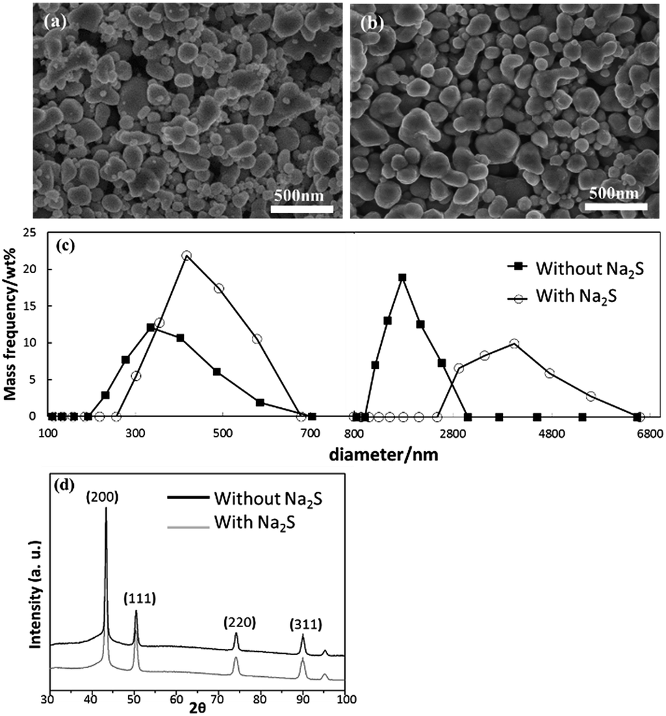 | ||
| Fig. 2 FE-SEM micrographs of Cu particles prepared without additive (a) and with additive (b), size distribution (c) and XRD pattern (d) of Cu particles. | ||
The two copper pastes were coated on the PET substrates with a size of 5 mm × 30 mm and dried in air for 5–10 minutes, and then treated with plasma at 300 W power. Three samples were treated for every condition to minimize error. Fig. 3 shows that the average resistivity evolution depended on the treatment time. It was found that the resistivity of the copper patterns generally decreased with the treatment time from an insulated state to high conductivity. At three minutes, the electrical resistivity was high and about 240 and 119 μΩ cm for the pastes with and without the Na2S additive, respectively. After that the resistivity drastically decreased to 40–50 μΩ cm in the two pastes. Further extension of the treatment time to over 20 minutes meant the resistivity slightly increased but it was still in the dozens of μΩ cm. As mentioned above, the copper without the Na2S additive included many small and big copper particles. Small nanoparticles are favored for sintering at low temperature. It agrees that these small Cu nanoparticles were sintered altogether in the beginning to achieve the high conductivity. For the Cu paste with the Na2S additive, the resistivity at three minutes was at a high of 240 μΩ cm. It related to the big and wide particle distribution shown in Fig. 2. However, with prolonging the treatment, these Cu patterns achieved a low resistivity of about 40 μΩ cm, which was lower than that of 49 μΩ cm for the Cu paste without the Na2S additive. The improvement might be attributed to the morphology of the Cu particles. From Fig. 2a and b, it suggests that the surface of the Cu particle was completely different. The former showed a sharp and clean-like surface, while the latter showed a rough and blurred surface. The rough surface means an increased surface area which is attributed to the sintering to achieve the high conductivity with treatment time. However, too long a treatment time caused a slight increase in the two copper pastes, which will be discussed later. However, these results suggest that the samples with the Na2S additive achieved high performance Cu patterns even with a big particle size and wide size distribution. It implies that suitable size design is key for high conductivity metal patterns.
 | ||
| Fig. 3 Resistivity of Cu patterns treated with plasma at 300 W. | ||
Fig. 4 gives the SEM images of the two Cu pastes after treatment with different times. At three minutes, the small particles in the Cu paste without Na2S were annealed and connected together, some small particles seem to melt into a big one or attach to a big particle. The particles in the Cu paste with Na2S, were also connected together but they still kept their original morphology, which suggested low resistivity in the former and high resistivity in the latter. When the treatment time was prolonged to 10 minutes, these Cu particles were further sintered to form a big grain size, which was attributed to the decreasing resistivity. When comparing the grain size, it was bigger in the Cu paste with Na2S than without the Na2S additive paste, which agreed with the lower resistivity (Fig. 3). When the treatment time was lengthened to over 20 minutes, some big voids seemed to occur although the grain size was further improved, which was consistent with the increase in resistivity for those Cu patterns. These voids might originate for two reasons, one might be the evaporation of organic compounds in the paste and substrates because plasma always cleans or reacts with those organic compounds. A long reaction time accelerated the production of organics to make large escaping spaces like voids. Another reason might be related to the stress coming from excessive sintering and a mismatched thermal expansion coefficient between copper and the substrates, which induced ruptures in the Cu pattern leading to high resistivity. However, the paste with the Na2S additive seems to achieve high conductivity in the plasma treatment process.
 | ||
| Fig. 4 Surface SEM images of the Cu pattern with Na2S sintered for 3 min (a), 10 min (b), 20 min (c) and without Na2S for 3 min (d), 10 min (e), 20 min (f) with the power at 300 W. | ||
Except for the treatment time, the power of the plasma is also an important parameter to make high conductivity Cu patterns. The Cu paste with the Na2S additive was used to optimize the plasma parameters. Fig. 5 shows the electrical resistivity of the Cu patterns with different power. The resistivity of the Cu patterns was decreased depending on the treatment time and applied power. For example, the Cu patterns presented the same high resistivity with only three minutes treatment with different power. When prolonging the treatment time, all of the Cu patterns showed a sharp decline in resistivity. It was very rapid in the low power case in the first ten minutes when compared to the high power case. After that, the resistivity was slightly increased when the power was over 200 W. In contrast, the resistivity was generally decreased with a low power of 100 W, however, only high resistivity Cu patterns were obtained. A lowest resistivity of about 15.9 μΩ cm was achieved at ten minutes with 200 W, which is superior to other reports.
 | ||
| Fig. 5 Electrical resistivity of Cu patterns depending on the plasma power and treatment time. | ||
Fig. 6 shows the surface and cross-section SEM micrographs of the Cu patterns after the RIE process with the power of 200 W for different times. As mentioned above, the sintering phenomenon clearly evolved with time. At three minutes, the neck growth between the particles started, especially for the small particles. With extending time, the neck growth was further enhanced to make a big grain size and gradually form a denser structure, which is attributed to the sharp decrease in resistivity seen in Fig. 5 at 10 min. When the time was extended to about 20 min, no significant difference was observed when comparing to the 10 min treated sample, which indicates that the real sintering process might be finished in about 10 min as mentioned above. It is known that the sintering phenomenon also is similar to the Ostwald ripening process, and suggests that the formation of a cluster corresponds to a decrease of total interfacial free energy between the small particle phases. In our case, high energy reactive plasma species bombarded the surface of the Cu particle and reacted with the organic layer covered on the surface of the Cu particles. These organics were cut or decomposed into smaller molecules or became gaseous, and escaped or evaporated to leave a very clean, active copper surface. Without the protection of the organic layer, the metal particles directly contacted with each other and then formed a big grain size or neck-growth due to surface atomic diffusion. The cross-section images also show that the neck-growth was enhanced with sintering time. And those small Cu particles were sintered together to become a big one from 3 to 10 min, after that no clear change was seen. It should be noted that these Cu patterns were a porous structure. Although the neck-growth achieved a conductive path which contributed to the current flowing, increasing the porous volume also weakened the path when compared to bulk copper. These voids originated from those organics escaping from the Cu surface which especially corresponded to the high plasma power due to excessive sintering, as mentioned above. With the power too high, a large amount of organics release made the big voids seen in Fig. 4, which led to high resistivity. Therefore, it is crucial to adjust the plasma parameters for the improvement of the Cu patterns.
 | ||
| Fig. 6 Surface and cross-section SEM micrographs of Cu patterns after the plasma process with the power at 200 W for 3 min (a and d), 10 min (b and e) and 20 min (c and f). | ||
For comparison, a standard plasma etching (PE) model was used to sinter these copper patterns. The resistivity difference of the copper patterns with the PE and RIE model is illustrated in Fig. S1.† The resistivity decreased with the treatment time, however, the applied power was very different. In the PE model, the Cu patterns were insulating when the power was low (below 500 W) even when treated for 20 min. When the applied power was 1000 W, the same evolution trend for resistivity was observed, however, it was still higher when compared to the RIE model with only 200 W power. From the cross-sections of the copper patterns (Fig. S2†), it was found that the sintering thickness was completely different in the two models. Although the surface of the Cu patterns was sintered together to make a big grain size, the substrate-side kept the original state with individual Cu particles in the PE model (Fig. S2†). On the contrary, apart from the surface-side, the substrate-side also suggests that many big-particles were grown with the RIE model (Fig. S3†). Moreover, the surface images of the RIE (Fig. 6) and PE models (Fig. S4†) were also distinguished. The grain size is still smaller in the PE model than the RIE model. It was clear that the surface in the PE model included some individual Cu particles without any changes. The results might be related to the different plasma reactions in the two models. The plasma species induced in the PE model were always freely distributed in the space of the chamber, and always invaded the Cu patterns from the surface and then generally permeated depending on the plasma power and the state of the Cu patterns. Hence, enough time was needed for the deeper sintering of the Cu patterns to decrease the resistivity, as seen in Fig. S1.† On the contrary, in the RIE model, a strong high frequency electric field was introduced to direct and accelerate the flow of plasma species to go into the Cu patterns, which rapidly and wholly sintered the Cu patterns. A low resistivity Cu pattern was obtained with a short sintering time even with low power (Fig. 5). A simple schematic diagram of the sintering mechanism in the two models is shown in Fig. S5.† However, the enhanced species flow might decompose the substrate to make contaminants or excessively sinter the Cu patterns to cause increasing resistivity (seen in Fig. 3 and 5). These results suggests that the RIE model was beneficial to the sintering of Cu patterns with short time and low power. Also it should be noted that a high power always increased the sample temperature with treatment time. For example, the temperature was over 100 °C when the treatment time was over 10 minutes, or even 120 °C with 20 minutes with the PE model and 1000 W. The temperature was only 75 °C when the treatment time was 10 minutes with the RIE model and 200 W. By combining the resistivity results of the Cu patterns, it shows that the RIE plasma model was a suitable and simple sintering method for many heat-sensitive substrates, which will largely spread the application of cheap copper paste in many intelligent next-generation devices.
In order to fabricate a flexible antenna, a V-shape antenna structure based on the Cu particles was printed onto a PET film and sintered with the RIE model. The thickness and resistivity of the antenna were about 10 μm and 20 μΩ cm, respectively. The return losses of these V-shaped antennas were evaluated at 0.5–4.0 GHz and are shown in Fig. 7. The frequency bands of the resonance peaks depended on the antenna length and a longer antenna corresponded to a higher frequency band.30 In our case, the length of the V-shaped antenna was 40 mm and the corresponding resonance peaks were located at around 2 GHz. Highly sensitive antennas should have low return losses at their resonance point, which are effected by the performance of the antenna, such as conductivity, surface roughness and so on. The copper pattern had a resonance point of about −22.2 dB, which was almost the same as a bulk copper foil antenna31 and far smaller than Cu-tape foil (shown in the Fig. 7). Smaller resonance points indicate a smaller signal power loss, which results from the reflection of the signal in the Cu pattern. The results suggest that our Cu pattern treated with plasma had the same performance as copper foil, and can replace the bulk Cu antennas used in many existing devices. Moreover, the Cu patterns fabricated with the Cu paste can be developed with various simple and easy printing techniques and applied in many flexible and wearable devices. Considering the low cost and simple sintering method of the Cu paste, Cu also is a suitable alternative to a silver antenna.
 | ||
| Fig. 7 The photo (a) and return loss (b) of the Cu V-shape pattern antenna. | ||
Conclusion
Sub-micro copper particles with different sizes and size distributions were successfully synthesized by a simple large scale polyol process with a trace amount of the Na2S additive. A Cu-paste based on these sub-micro copper particles was made and printed on flexible polymer substrates in air. A plasma technique was used to sinter these copper patterns in a vacuum chamber with the flow of argon and hydrogen. The resistivity of these copper patterns depended on the plasma model, power and treatment time. The copper patterns formed with Na2S additive Cu-paste always achieved low resistivity when compared to the Cu-paste without the additive, which corresponded to the size and size distribution of these sub-micro copper particles. The normal PE model plasma always gave high resistivity copper patterns when compared to the RIE model. A Cu pattern with a resistivity of 15.9 μΩ cm was achieved with RIE plasma treatment at 200 W and with only 10 min. Moreover, the temperature of the copper pattern treated with the RIE model plasma only had a slight increase up to 75 °C, which was far lower than the damage temperature of many polymer substrates. An antenna based Cu pattern was evaluated and it had the same high performance as copper foil. These results indicate that the cheap and large-scale synthesis of sub-micro Cu-paste can be used in many wearable devices to substitute an Ag pattern.Acknowledgements
This work was partly supported by the COI Stream Project, and Grant-in-Aid for Scientific Research (Kaken S, 24226017). The authors thank very much for the experiment support from DENSHI GIKEN Co., Ltd. in Japan, they have provided the plasma equipment and given many helpful comments about the plasma sintering. H. Zhang acknowledges the financial support from China Scholarship Council for his PhD research in Osaka University.References
- T. Araki, T. Sugahara, J. Jiu, S. Nagao, M. Nogi, H. Koga, H. Uchida, K. Shinozaki and K. Suganuma, Langmuir, 2013, 29, 11192–11197 CrossRef CAS PubMed.
- Y. Chen, J. Au, P. Kazlas, A. Ritenour, H. Gates and M. McCreary, Nature, 2003, 423, 136 CrossRef CAS PubMed.
- H. Okimoto, T. Takenobu, K. Yanagi, Y. Miyata, H. Shimotani, H. Kataura and Y. Iwasa, Adv. Mater., 2010, 22, 3981–3986 CrossRef CAS PubMed.
- S. H. Lim, J. W. Kemling, L. Feng and K. S. Suslick, Analyst, 2009, 134, 2453–2457 RSC.
- K. Otte, L. Makhova, A. Braun and I. Konovalov, Thin Solid Films, 2006, 511, 613–622 CrossRef PubMed.
- V. Subramanian, J. M. Fréchet, P. C. Chang, D. C. Huang, J. B. Lee, S. E. Molesa, A. R. Murphy, D. R. Redinger and S. K. Volkman, Proc. IEEE, 2005, 93, 1330–1338 CrossRef CAS.
- J. Perelaer, R. Abbel, S. Wünscher, R. Jani, T. van Lammeren and U. S. Schubert, Adv. Mater., 2012, 24, 2620–2625 CrossRef CAS PubMed.
- K. Yung, X. Gu, C. Lee and H. Choy, J. Mater. Process. Technol., 2010, 210, 2268–2272 CrossRef CAS PubMed.
- I. Reinhold, C. E. Hendriks, R. Eckardt, J. M. Kranenburg, J. Perelaer, R. R. Baumann and U. S. Schubert, J. Mater. Chem., 2009, 19, 3384–3388 RSC.
- S. Wünscher, S. Stumpf, A. Teichler, O. Pabst, J. Perelaer, E. Beckert and U. S. Schubert, J. Mater. Chem., 2012, 22, 24569–24576 RSC.
- S. Magdassi, M. Grouchko and A. Kamyshny, Materials, 2010, 3, 4626–4638 CrossRef CAS PubMed.
- S. Jang, Y. Seo, J. Choi, T. Kim, J. Cho, S. Kim and D. Kim, Scr. Mater., 2010, 62, 258–261 CrossRef CAS PubMed.
- E. Yu, L. Piao and S. Kim, Bull. Korean Chem. Soc., 2011, 32, 4099–4102 CrossRef CAS.
- J. Ryu, H.-S. Kim and H. T. Hahn, J. Electron. Mater., 2011, 40, 42–50 CrossRef CAS.
- M. Zenou, O. Ermak, A. Saar and Z. Kotler, J. Phys. D: Appl. Phys., 2014, 47, 025501 CrossRef.
- G. Saito, S. Hosokai, M. Tsubota and T. Akiyama, J. Appl. Phys., 2011, 110, 023302 CrossRef PubMed.
- S.-H. Kwon, D.-H. Han, H. J. Choe and J.-J. Lee, Nanotechnology, 2011, 22, 245608 CrossRef PubMed.
- H. Lee, S. H. Park, S.-G. Seo, S.-J. Kim, S.-C. Kim, Y.-K. Park and S.-C. Jung, Curr. Nanosci., 2014, 10, 7–10 CrossRef CAS.
- S. Wünscher, R. Abbel, J. Perelaer and U. S. Schubert, J. Mater. Chem. C, 2014, 2, 10232–10261 RSC.
- Y. Matsumoto, Y. Yamaguchi, J. Hombo, T. Hauber and W. Göpel, J. Solid State Chem., 1992, 98, 201–205 CrossRef CAS.
- J. Jiu, K. Murai, D. Kim, K. Kim and K. Suganuma, Mater. Chem. Phys., 2009, 114, 333–338 CrossRef CAS PubMed.
- S. E. Skrabalak, L. Au, X. Li and Y. Xia, Nat. Protoc., 2007, 2, 2182–2190 CrossRef CAS PubMed.
- D. Ung, G. Viau, C. Ricolleau, F. Warmont, P. Gredin and F. Fievet, Adv. Mater., 2005, 17, 338–344 CrossRef CAS PubMed.
- J. L. C. Huaman, K. Sato, S. Kurita, T. Matsumoto and B. Jeyadevan, J. Mater. Chem., 2011, 21, 7062–7069 RSC.
- K. E. Korte, S. E. Skrabalak and Y. Xia, J. Mater. Chem., 2008, 18, 437–441 RSC.
- J. Jiu, K. Murai, K. Kim and K. Suganuma, J. Mater. Sci.: Mater. Electron., 2010, 21, 713–718 CrossRef CAS.
- T. Zhao, J.-B. Fan, J. Cui, J.-H. Liu, X.-B. Xu and M.-Q. Zhu, Chem. Phys. Lett., 2011, 501, 414–418 CrossRef CAS PubMed.
- A. R. Siekkinen, J. M. McLellan, J. Chen and Y. Xia, Chem. Phys. Lett., 2006, 432, 491–496 CrossRef CAS PubMed.
- Z. Li, A. Gu, M. Guan, Q. Zhou and T. Shang, Colloid Polym. Sci., 2010, 288, 1185–1191 CAS.
- M. Nogpasteomoda, K. Otsuka and K. Suganuma, Nanoscale, 2013, 5, 4395–4399 RSC.
- N. Komoda, M. Nogi, K. Suganuma and K. Otsuka, ACS Appl. Mater. Interfaces, 2012, 4, 5732–5736 CAS.
Footnote |
| † Electronic supplementary information (ESI) available. See DOI: 10.1039/c5ra18583a |
| This journal is © The Royal Society of Chemistry 2015 |