CuInSe2 thin film solar cells prepared by low-cost electrodeposition techniques from a non-aqueous bath

Priyanka U. Londhe, Ashwini B. Rohom and Nandu B. Chaure*
Department of Physics, Savitribai Phule Pune University (formerly University of Pune), Pune-411007, India. E-mail: n.chaure@physics.unipune.ac.in; Fax: +91 20 2569 1684; Tel: +91 20 2569 9072

Received 8th September 2015 , Accepted 14th October 2015

First published on 14th October 2015


Abstract

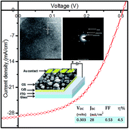
Polycrystalline CuInSe2 (CIS) thin films have been prepared by low-cost electrochemical method from non-aqueous ethylene glycol solvent onto cadmium sulfide (CdS) thin films. The co-deposition potential for Cu, In and Se was optimized with cyclic voltammetry measurements. CIS layers were electrodeposited at −1.1, −1.3 and −1.5 V versus Ag/AgCl references in an air-tight custom made electrodeposition cell. The films were selenized at 400 °C for 20 minutes. The optical, structural, morphological, compositional and optoelectronic properties of as-prepared and selenized samples were studied using UV-Vis spectrophotometery, X-ray diffractometery, transmission electron microscopy (TEM), scanning electron microscopy (SEM), energy dispersive X-ray analysis (EDAX) and current–voltage (IV) measurements. Three prominent sharp peaks of tetragonal CIS, (112), (204)/(220), and (312/116) were revealed in all as-prepared and selenized samples. Upon selenization the crystallinity of the samples was found to be improved remarkably. Compact, void free, and nearly uniform thin films of grain size ∼1 μm were deposited. The as-deposited and selenized CIS samples were Cu-rich whereas the content of Se was ∼50% obtained by EDAX analysis. The value of inter-planer distance, d = 3.339 Å, measured by HRTEM corresponds to the (112) plane of a tetragonal CIS crystal structure. The circular spotted rings observed in the selected area diffraction (SAD) pattern were confirmed as (112), (204)/(220) and (312)/(116) reflections of CIS. The solar cell parameters, Voc, Jsc, FF and efficiency (η) were found to be 303 mV, 28 mA cm−2, FF ∼ 53% and η = 4.5% for the CIS film deposited at −1.5 V. The values of shunt conductance, GD = 2.5 mS cm−2 and GL = 7.9 mS cm−2 and series resistance, RD = 0.81 Ω cm2 and RL = 0.19 Ω cm2 were calculated for dark and illuminated conditions. Mott–Schottky analysis was also carried out on the final solar cell in dark and illuminated conditions to study the carrier concentration and defects in the CdS/CIS interface.


Introduction

Chalcopyrite I–III–VI2 compounds have been the topic of intense research in recent years. Polycrystalline CuInSe2 (CIS) based absorber materials have emerged as leading candidate in thin film solar cell technology due to their applicability as absorber materials for highly efficient and cost effective solar electricity generation. Ideally, the absorber material of an efficient terrestrial photovoltaic cell should have a direct energy band gap in the range 1.2–1.5 eV, high optical absorption coefficient, and long diffusion length of minority carriers, which is fulfilled by CIS with Ga doping. Solar cells based on CIGS fabricated by vacuum evaporation technique are currently leading in terms of conversion efficiency of around 21.7% on the laboratory scale.1 CIS and CIGS can be deposited using vacuum deposition techniques like sputtering,2 co-evaporation,3 flash evaporation,4 molecular beam epitaxy,5 pulsed laser deposition6 and stacking elemental layers,7 which are reasonably expensive due to the capital investment and use of highly pure source materials. Highly crystalline and controlled stoichiometric binary, ternary and quaternary semiconductor thin films can be prepared by vacuum techniques, however the technical issues such as deposition over a large area and slow deposition rate, are unresolved. A non-vacuum technique such as, spray paralysis,8 chemical bath deposition (CBD),9 sol–gel and electrodeposition (ED)10–13 have also been used successfully for the preparation of CIS thin films. Electrodeposition is one of the low-cost techniques to deposit semiconductor/metal films over large area with high deposition rate. The controlled stoichiometry can be maintained in the precursor layer by electrochemical deposition.14 One step, multi-step, pulsed, stacked layer electrodeposition techniques are commonly adapted to prepared CIS, CIGS and CZTS chalcopyrite thin films.15–20 The power conversion efficiency 7.0% is reported by Qiu et al.21 using one-step electrodeposition from aqueous bath. A non-aqueous electrolyte can be used to deposit semiconductor, oxide and insulator thin films, which allows depositing layer at higher growth potentials which can be limited in aqueous medium due to hydrogen evolution. Besides this the layers can be deposited for higher bath temperature to enhance the homogeneity, crystallinity and particle size. There have been a very few reports available on the electrodeposition of CIS from non-aqueous medium.22–24 Bhattacharya et al.22 has reported the basic studies on the growth of CIGS from dimethyl sulfoxide (DMSO). Dharmadasa et al.22 have used ethylene glycol as a solvent to electrodeposit CIS thin film however, they have not reported the development solar cells. Nevertheless, the similar electrolyte had been used previously in the literature to prepare the CdTe,25 CdHgTe26 and CdZnTe27 material and their solar cell.

In the present studies we have potentiostatically electrodeposited CIS thin films from non-aqueous (ethylene glycol) bath onto cadmium sulfide thin films and investigated the effect of deposition potential on optical, structural, morphology and composition properties of CIS layer. The as-prepared CIS layers electrodeposited from ethylene glycol at high bath temperature (130 °C) are highly crystalline with large grains as compare to the layers prepared from aqueous bath.28 The reported procedure could be helpful to produce the low-cost solar cell devices on plastic (flexible) substrate.

Experimental details

CIS thin films were potentiostatically electrodeposited in ethylene glycol onto CdS substrates at 130 °C using Biologic potentiostat/galvanostat model SP150. CdS thin films were prepared by chemical bath deposition method on fluorine doped tin oxide (FTO) coated glass substrates. The detailed study is reported elsewhere.29 Prior to cyclic voltammetry (CV) and deposition of CIS, CdS layers were annealed at 400 °C for 20 min. A conventional three-electrode geometry with Ag/AgCl as reference, CdS coated on FTO as working and graphite as counter electrode were used. CuCl2, InCl3 and SeCl4 purchased from Sigma-Aldrich of purity at least 99.9% were used as received. LiCl was used as a supporting chemical compound to control the ionic conductivity of bath. Three different potentials, −1.1, −1.3 and −1.5 V versus Ag/AgCl reference optimized by CV measurement were chosen to electrodeposit CIS thin films. The temperature of bath was maintained at 130 °C during CV measurements and growth of thin films without agitation. The samples were selenized in a home-made selenization chamber at 400 °C for 20 min. Selenized CdS/CIS samples were etched in Br–methanol and NaCN solution to remove the unwanted secondary phases of Cu and Se. Finally, a circular Au contact of area 3 mm diameter were made by vacuum evaporation technique. The structural properties of films were studied by X-ray diffractometer, Model Bruker D8, with CuKα radiation of wavelength 1.5405 Å. The presence of crystallographic planes and inter-planner distance was measured directly with the help of transmission electron microscopy (TEM) model, TECNAI G2. The film morphology was examined using JEOL JSM-6360A Scanning electron microscopy (SEM) at accelerating voltage 20 kV and probe current 1 nA. The EDAX attachment available in above SEM instrument was employed to obtain the compositional analysis. The optical properties were studied by using JASCO UV-Vis-NIR spectrophotometer. IV and CV measurement were performed using Biologic Potentiostat attached with probe station and necessary software. The optoelectronic properties of complete solar cell device were measured under illumination with power intensity 100 mW cm−2 at room temperature ∼25 °C. Incident-photon-to-current conversion efficiency (IPCE) was measured by photon counting spectrometer, ISS Inc., and Kiethley 2400 source meter.

Results and discussion

CV measurement was carried out to investigate the electrochemical processes during electrodeposition of CuInSe2 in the range 0 V to −2.0 V versus Ag/AgCl reference electrode. The cyclic voltammogram recorded with scan 10 mV s−1 on CdS substrate without agitation is depicted in Fig. 1. Cathodic and anodic scans are marked by forward and reverse arrows, respectively. CV measurement was begin at 0 V to avoid the stripping of CdS layer, therefore the initial feature related to the reduction of Cu and Se have not been observed. A cathodic current was initially found to be increased could be due to the elemental deposition of Cu and/or Se by the following charge transfer reaction;
 
Cu2+ + 2e → Cu, Eo = +0.34 V versus SCE (1)
 
Se4+ + 4e → Se, Eo = +0.84 V versus SCE (2)
and/or
 
Se4+ + 6e → Se2−, Eo = +0.048 V versus SCE (3)

image file: c5ra18315d-f1.tif
Fig. 1 A typical cyclic voltammogram recorded in an electrolyte consisting ionic species CuCl2, InCl3 and SeCl4, with scan rate 10 mV s−1 at temperature 130 °C using Ag/AgCl reference electrode on CdS substrate. LiCl was used as supporting chemical compound to control the ionic conductivity of bath.

A plateau region observed up to −0.7 V is proposed due to the deposition of CuxSey compounds. Indeed, we have observed that the films electrodeposited in this region were brownish in color with powdery deposition. Further the cathodic current rises with increasing the cathodic potential due to the deposition of In along with Cu and Se by following charge transfer reaction,

 
In3+ + 3e → In, Eo = −0.34 V versus SCE (4)

An exponential increase in cathodic current beyond −1.0 V could be due to the co-deposition of Cu, In and Se. A sharp rise in the current around −1.0 V and higher cathodic potential was not observed, which confirms the absence of hydrogen evolution in non-aqueous bath. Note that we have not observed any bubbling from the cathode for higher cathodic potential up to −1.8 V versus Ag/AgCl. During anodic scan three different shoulder's observed at ∼−1.40 V, −0.85 V and −0.30 V are assigned for the stripping of In and Cu deposited at over potential depositions. The stripping peak of Se was not observed, which would be expected at lower cathodic potentials (+ve potential). As the clear plateau region was not observed in cyclic voltammogram, therefore, the CIS thin films have been electrodeposited at three different potentials −1.1 V, −1.3 V and −1.5 V versus Ag/AgCl onto CdS substrate.

The XRD pattern of as-prepared and selenized CIS films electrodeposited at −1.1 V, −1.3 V and −1.5 V on CdS substrate is depicted in Fig. 2A and B, respectively.


image file: c5ra18315d-f2.tif
Fig. 2 X-ray diffractogram of the CIS thin film deposited at −1.1 V (a), −1.3 V (b) and −1.5 V (c), [A] as-prepared and [B] selenized XRD spectra of the CIS layers deposited at above growth potentials.

Highly polycrystalline CIS thin films preferentially oriented along (112) plane are obtained for all growth potentials. Three prominent peaks corresponds to (112), (204)/(220) and (312)/(116) reflection are observed in as-prepared samples. A wider base observed in as-prepared CIS sample deposited at −1.1 V for reflections (112) and (204/220) is due to the presence of secondary phases of Cu2Se3 (JCPDS Card no. 72-1421) marked as solid square (■). The reflections associated to FTO are marked as solid circle (●). CIS sample electrodeposited at −1.5 V on to CdS substrate was found to be highly crystalline without secondary phases of CuxSey. Upon selenization the peak corresponds to CdS (101) reflection (JCPDS Card no. 41-1041) was attributed at 2θ = 28.20°. The crystallinity of as-prepared CIS thin films deposited for −1.3 V and −1.5 V in non-aqueous bath is much higher than the annealed CIS samples prepared in aqueous bath.28 Therefore, the electrodeposition of CIS in non-aqueous bath may be useful for the development of solar cell on flexible substrates without heat treatment or selenization.

The secondary peaks associated to CuxSey were not attributed after selenization in all samples grown at different potentials. An enhancement in the crystallinity of CIS peak was further observed upon selenization. The full width at half maximum (FWHM) calculated for (112) peak was found to be decreased substantially from 0.51°, 0.36° and 0.30° to 0.30°, 0.15° and 0.12° for the sample grown at −1.1 V, −1.3 V and −1.5 V, respectively. The enhancement in the crystallinity with selenization at higher temperature is proposed due to the re-crystallization of material along with the agglomeration of small grains.

The surface topographical images of as-prepared and selenized samples were recorded using the scanning electron microscope (SEM), Model-JEOL JSM-6360A. Fig. 3a–c are the SEM images of as-prepared CIS thin films deposited at potentials −1.1 V, −1.3 V and −1.5 V on to CdS substrates. The corresponding selenized images are depicted in Fig. 3d–f, respectively. The physical appearance of the samples was grayish-black in color with well adherent to the substrate.


image file: c5ra18315d-f3.tif
Fig. 3 SEM images of as-prepared (a–c) and the corresponding selenized (d–f) CIS films electrodeposited on at −1.1 V, −1.3 V and −1.5 V, respectively.

SEM images are clearly shows a void free deposition of CIS alloy over large area. The globular surface morphology of grain size ranging from ∼500 nm to l.5 μm was observed in the sample deposited at −1.1 V, whereas the mixed surface morphology consisting spherical particles as well as long needle like structure can be seen for the samples deposited at −1.3 V. Overgrowth of the particle of size ∼4–5 μm was observed for the sample deposited at −1.5 V. The overgrowth of the particle is associated to the mass-transfer coefficient. The large overgrowth is due to the higher deposition rate of diffusion limiting species. The deposition time for all samples was kept 30 minute. Diffused uniform grains can be clearly seen upon selenization. The enhancement observed in the grain is associated to the re-crystallization of material. The compositional analysis of as-prepared and selenized CIS thin films deposited for −1.1 V, −1.3 V and −1.5 V were obtained by EDAX. All as-prepared samples were Cu-rich and the content of Se was nearly similar close to 50 atomic percentages. After selenization the atomic percentage concentration of Cu was found to be reduced and nearly stoichiometric CIS thin films are obtained at −1.5 V growth potential. The Cu/In ratio was systematically decreased for selenized sample from 2.09 to 1.34 with increasing the cathodic potential. The elemental composition (atomic percentage) obtained by EDAX analysis is tabulated in Table 1.

Table 1 A summary of compositional analysis of CuInSe2 thin films electrodeposited on CdS substrate
Deposition potential versus Ag/AgCl (V) Composition (atomic percentage)
Cu In Se Cu/In ratio
As-deposited Selenized As-deposited Selenized As-deposited Selenized As-deposited Selenized
−1.1 36.10 35.81 22.00 17.10 41.91 47.10 1.64 2.09
−1.3 40.41 29.74 25.12 21.53 34.47 48.73 1.60 1.38
−1.5 35.13 28.62 26.46 21.30 38.41 50.09 1.33 1.34


Fig. 4 shows the plots of (αhν)2 versus energy () for CIS thin films deposited for −1.1 V, −1.3 V and −1.5 V versus Ag/AgCl reference. The optical band gap was found to be in the range of 1.06 eV to 1.01 eV (±0.05) and 0.98 eV to 0.95 eV (±0.05) for as-deposited and selenized samples, respectively. The band gap estimated for as-deposited and selenized sample was nearly similar within an error ± 0.05. Sharp fundamental absorption edge could be seen upon selenization. This could be due to the re-crystallization of thin films along with the homogeneous phase formation. The values of the band-gap estimated from the optical absorption spectra are summarized in Table 2.


image file: c5ra18315d-f4.tif
Fig. 4 Optical absorption spectra recoded for as-deposited and selenization (a–c) CIS thin film deposited on CdS at −1.1 V, −1.3 V and −1.5 V, respectively.
Table 2 A summary of band gap calculated for CuInSe2 thin films deposited on FTO/CdS at various deposition potentials
Deposition potential (V) Band gap (eV)
As-deposited Selenized
−1.1 V 1.06 ± 0.05 0.98 ± 0.05
−1.3 V 1.03 ± 0.05 0.96 ± 0.05
−1.5 V 1.01 ± 0.05 0.95 ± 0.05


Fig. 5 shows the HRTEM (a) and SAD pattern (b) of the selenized CIS thin film deposited at −1.5 V. The ‘d’ spacing obtained by HRTEM analysis is 3.339 Å, which corresponds to (112) reflection of tetragonal structure of CIS. Three dotted circular rings correspond to (112), (204)/(220) and (312)/(116) planes of CIS are observed is selected area diffraction pattern. This is in good agreement with the structural data obtained by XRD.


image file: c5ra18315d-f5.tif
Fig. 5 (a) HRTEM image of selenized CIS layer deposited at −1.5 V and the corresponding (b) selected area diffraction (SAD) pattern.

The film deposited at −1.5 V shows good optical and structural properties. Moreover, the stoichiometric CIS layers were obtained upon selenization. Therefore, we have studied the optoelectronic properties of CdS/CIS solar cell wherein CIS was electrodeposited at −1.5 V versus Ag/AgCl reference electrode. The most common tool for solar cell analysis is the current–voltage (JV) measurements under standard illumination 100 mW cm−2 (AM 1.5). The JV measurement results four solar cell parameters, short circuit current (Jsc), open circuit voltage (Voc), fill factor (FF) and power conversion efficiency (η), which are often used to characterize the photovoltaic device. Jsc depends on the absorption of photons and collection of carriers, whereas Voc is ruled by the band gap of the absorber and the degree of recombination in the cell. These parameters are well accepted indicators of solar cell performance and are particularly valuable for comparing and qualifying cells.

The JV behavior of a thin film solar cell (TFSC) can be described by a general single exponential diode equation,30

 
image file: c5ra18315d-t1.tif(5)
where R, the series resistance, and G shunt conductance that occur in series or parallel with the primary diode, respectively.

The behavior of device and diode parameters were studied with the plots of JV, dJ/dV versus V and dV/dJ versus (J + Jsc)−1, each comparing the data measured under dark and illumination conditions. Fig. 6 shows the current–voltage graph of CIS solar cell under dark and illuminated condition. The values of solar cell parameters (Jsc, Voc, FF and η) obtained from graph 6 are summarized in Table 3. The cross-over observed between the dark and illuminated IV curve, which is commonly seen in TFSC. This may be due to the defect states present in the absorber or at the hetero-interface or in the CdS layer.31–34 The stability of the absorber material (CIS) can be further improved by optimizing the selenization parameters, which will not only prevent the crossover but also improve the solar cell performance.


image file: c5ra18315d-f6.tif
Fig. 6 Dark and illuminated JV curves of CdS/CIS heterostructure solar cell device. CIS layer was electrodeposited at −1.5 V versus Ag/AgCl reference electrode.
Table 3 A solar cell parameters obtained under dark and illuminated conditions
Cell Voc (volts) Jsc (mA cm−2) FF η % GD (mS cm−2) GL (mS cm−2) RD Ω cm2 RL Ω cm2 nD nL ND cm−3 NL cm−3
FTO/CdS/CIS/Au 0.303 28 0.53 4.5 2.5 7.9 0.81 0.19 1.9 1.5 1.09 × 10¹⁶ 1.05 × 10¹⁸


Some non-ideal effects, such as current blocking behavior or light-to-dark crossover in forward bias or breakdown in reverse bias commonly observed in TFSCs are not explained by the JV curve. The plots of dJ/dV versus V, dV/dJ versus (J + Jsc)−1 are derived from the JV curves in dark and illuminated condition. The diode term in the eqn (5) becomes negligible for the plot dJ/dV against V (Fig. 7) near Jsc and in reverse bias. If the shunt term is ohmic and JL is constant, G(V) will be flat with the value in reverse bias equal to G. The values of G for dark and illuminated condition is found to be GD = 2.5 mS cm−2 and GL = 7.9 mS cm−2, respectively.


image file: c5ra18315d-f7.tif
Fig. 7 A graph of dJ/dV vs. V for CdS/CIS heterostructure solar cell device. The experimental data depicted in Fig. 6 is processed to obtain these graphs.

A plot of dV/dJ against (J + Jsc)−1 yield a straight line if JL is independent of voltage. A linear fit to the data gives an intercept to y-axis and slope are equivalent to series resistance ‘R’ and ideality factor ‘n’. The values of series resistance, RD and RL and ideality factor, nD and nL deduced from Fig. 8a and b under dark and illuminated condition, respectively are given Table 3. The suffix ‘D’ and ‘L’ indicates the parameters calculated for dark and illuminated condition of solar cell. Generally, the ideality factor is ∼2 when the recombination current dominates and ∼1 when the diffusion current dominates which determined for the forward bias current at lower potential region. The values of nD and nL have been found between 1 and 2 indicates both currents are comparable.35


image file: c5ra18315d-f8.tif
Fig. 8 A graph of dV/dJ vs. (J + Jsc)−1 for CdS/CIS solar measured in dark (a) and illuminated (b) conditions. The experimental data depicted in Fig. 6 is processed to obtain these graphs.

The IPCE measurement of the above solar cell device was performed and results are depicted in Fig. 9. The CIS cell exhibited a high response to visible light in the wavelength 450–600 nm. However, in the near-infrared wavelength region the IPCE response was poor. The loss in the IPCE for higher wavelength (<600 nm) region could be due to the thin (1.5–2 μm) CIS absorber layer. Thin absorber layer directly affect the absorption coefficient, which gives rise to the incomplete generation of electron–hole pair in CIS layer.30 The other reason for the loss in QE in the above region may be the trap states (defects) present in the bulk CIS layer, which leads to the recombination of electrons and holes.


image file: c5ra18315d-f9.tif
Fig. 9 Incident photon-to-current efficiency (IPCE) curve for superstrate (FTO/CdS/CIS/Au) structured solar cell.

CV measurement on diode is normally analyzed using the depletion approximation. According to this approximation the capacitance response of the junction originates solely from the edge of the depletion region which means that the junction is modeled as a plate capacitor.

For an ideal abrupt homo-junction diode the inverse of the capacitance is given by

 
image file: c5ra18315d-t2.tif(6)
where, q is the unit charge, εs the static permittivity of semiconductor, Vbi the built-in voltage and V the applied voltage. The value of εs is calculated by considering the dielectric constant of material, εr = 13.5 36 and the permittivity of free space, εo.

Ideally, it yields a straight line whose intersect with the voltage axis gives the junction built in potential and slope determines the acceptor concentration of the absorber material. The Fig. 10a and b represents the Mott–Schottky plots for CdS/CIS thin film solar cell device measured under dark and illuminated conditions, respectively. The calculated values of carrier density in dark (NAD) and illuminated (NAL) condition are consistent with reported values for CIS prepared by various methods.12,37–39 As expected the higher carrier density was obtained upon illumination of solar cell. These values are tabulated in Table 3. Capacitance under illumination was found to be increased could be due to the trapping of photo generated charge carriers at the irrelevant states within the band gap.


image file: c5ra18315d-f10.tif
Fig. 10 Mott–Schottky, 1/C2 versus voltage plot for CdS/CIS thin film solar cell, (a) dark and (b) illuminated condition recorded for frequency 50 kHz.

Conclusion

Highly polycrystalline chalcopyrite CIS thin films have been electrodeposited from non-aqueous bath on CdS substrates for higher cathodic potentials (∼1.5 V) versus Ag/AgCl reference electrode. This process could be effective for the electrodeposition of CIGS thin films, where the deposition of Ga is difficult along with Cu, In and Se. Selenization procedure not only support to enhance the crystallinity but also helped to obtained nearly stoichiometric CIS films. The sharp fundamental absorption edge with energy gap ∼0.98 (±0.05) eV was estimated from selenized CIS thin films. Compact, well adherent and void free CIS layers were electrodeposited for all reported potentials. The dotted circular rings correspond to (112), (204)/(220) and (312)/(116) planes of tetragonal CIS are revealed in SAD pattern. The inter-planer distance ‘d’ obtained by HRTEM corresponds to (112) reflection of CIS. The solar cell parameters, Voc, Jsc, FF and efficiency were found to be 303 mV, 28 mA cm−2 and FF ∼ 53% and η = 4.5% for the CIS film deposited at −1.5 V. The values of shunt conductance, GD = 2.5 mS cm−2 and GL = 7.9 mS cm−2 and series resistance, RD = 0.81 Ω cm2 and RL = 0.19 Ω cm2 were calculated for dark and illuminated conditions. The increased capacitance observed in Mott–Schottky plot upon illumination may be due the presence of trap states (defects) within the material or at the interface.

Acknowledgements

The authors would like to thank the Defence research and development organization (DRDO), New Delhi, India (ERIP/ER/10003866/M/01/1388) for providing the financial support under major research grant.

References

  1. M. A. Green, K. Emery, Y. Hishikawa, W. Warta and E. D. Dunlop, Progress in Photovoltaics : Research and Applications, 2015, 23, 1–9 CrossRef PubMed.
  2. R. Ingrid, A. C. Miguel, E. Brian, B. Egaas, C. DeHart, J. Scharf, C. L. Perkins, B. To and R. Noufi, Progress in Photovoltaics : Research and Applications, 2008, 16, 235–239 CrossRef PubMed.
  3. A. H. Moharram, M. M. Hafiz and A. Salem, Appl. Surf. Sci., 2001, 172, 61–67 CrossRef CAS.
  4. A. Ashida, Y. Hachiuma, N. Yamamoyo and Y. Cho, J. Mater. Sci. Lett., 1994, 13, 1181–1184 CrossRef CAS.
  5. S. Niki, A. Yamada, R. Hunger, P. J. Fonsa, K. Iwataa, K. Matsubara, A. Nishiob and H. Nakanishi, J. Cryst. Growth, 2002, 237–239, 1993–1999 CrossRef CAS.
  6. X. L. Wang, G. J. Wang, B. L. Tian and Z. L. Du, Chin. Sci. Bull., 2010, 55, 1854–1858 CrossRef CAS.
  7. A. N. Tiwari, M. Krejci, F. J. Haug and H. Zogg, Progress in Photovoltaics : Research and Applications, 1999, 7, 393–397 CrossRef CAS.
  8. T. Terasako, Y. Uno, T. Kariya and S. Shirakata, Sol. Energy Mater. Sol. Cells, 2006, 90, 262–275 CrossRef CAS PubMed.
  9. H. M. Pathan and C. D. Lokhande, Appl. Surf. Sci., 2005, 245, 328–334 CrossRef CAS PubMed.
  10. H. Lee, W. Lee, J. Kim, M. Ko, K. Kim, K. Seo, D. Lee and H. Kim, Electrochim. Acta, 2013, 87, 450–456 CrossRef CAS PubMed.
  11. R. N. Bhattacharya, J. Electrochem. Soc., 1983, 130, 2040–2042 CrossRef CAS PubMed.
  12. N. B. Chaure, A. P. Samantilleke, R. P. Burton, J. Young and I. M. Dharmadasa, Thin Solid Films, 2005, 472, 212–216 CrossRef CAS PubMed.
  13. X. Donglin, X. Man, L. J. Zhuang and Z. Xiujian, J. Mater. Sci., 2006, 41, 1875–1878 CrossRef.
  14. N. B. Chaure, J. Young, A. P. Samantilleke and I. M. Dharmadasa, Sol. Energy Mater. Sol. Cells, 2004, 81, 125–133 CrossRef CAS PubMed.
  15. J. Tao, J. Liu, J. He, K. Zhang, J. Jiang, L. Sun, P. Yang and J. Chu, RSC Adv., 2014, 4, 23977–23984 RSC.
  16. J. Tao, K. Zhang, C. Zhang, L. Chen, H. Cao, J. Liu, J. Jiang, L. Sun, P. Yang and J. Chu, Chem. Commun., 2015, 51, 10337–10340 RSC.
  17. J. C. Malaquias, D. Regesch, P. J. Dale and M. Steichen, Phys. Chem. Chem. Phys., 2014, 16, 2561 RSC.
  18. A. B. Rohom, P. U. Londhe and N. B. Chaure, J. Solid State Electrochem., 2015, 19, 201–210 CrossRef CAS.
  19. M. Lakhe and N. B. Chaure, Sol. Energy Mater. Sol. Cells, 2014, 123, 122–129 CrossRef CAS PubMed.
  20. P. U. Londhe, A. B. Rohom and N. B. Chaure, J. Mater. Sci.: Mater. Electron., 2014, 25, 4643–4649 CrossRef CAS.
  21. S. N. Qiu, L. Li, C. X. Qiu, I. Shih and C. H. Champness, Sol. Energy Mater. Sol. Cells, 1995, 37, 389–393 CrossRef CAS.
  22. R. N. Bhattacharya, M. A. Contreras, J. Keane, A. L. Tennant, J. R. Tuttle, K. Ramanathan and R. Noufi, US Pat., 5 804 054, 1998.
  23. J. S. Wellings, A. P. Samantilleke, S. N. Heavens, P. Warren and I. M. Dharmadasa, Sol. Energy Mater. Sol. Cells, 2009, 93, 1518–1523 CrossRef CAS PubMed.
  24. N. B. Chaure, J. Renewable Sustainable Energy, 2013, 5, 0316041–0316047 Search PubMed.
  25. R. K. Pandey, S. Maffi and L. P. Bicelli, Mater. Chem. Phys., 1993, 35, 15–20 CrossRef CAS.
  26. J. P. Nair, R. Jayakrishnan, N. B. Chaure, S. Gohkale, A. Lobo, S. K. Kulkarni and R. K. Pandey, J. Phys. Chem. Solids, 1999, 60, 1693–1703 CrossRef CAS.
  27. N. B. Chaure, S. Chaure and R. K. Pandey, Electrochim. Acta, 2008, 54, 296–304 CrossRef CAS PubMed.
  28. N. B. Chaure, J. Young, A. P. Samantilleke and I. M. Dharmadasa, Sol. Energy Mater. Sol. Cells, 2004, 81, 125–133 CrossRef CAS PubMed.
  29. N. B. Chaure, S. Bordas, A. P. Samantilleke, S. N. Chaure, J. Haigh and I. M. Dharmadasa, Thin Solid Films, 2003, 437, 10–17 CrossRef CAS.
  30. S. S. Hegedus and W. N. Shafarman, Progress in Photovoltaics : Research and Applications, 2004, 12, 155–176 CrossRef CAS PubMed.
  31. M. Nichterwitz, R. Caballero, C. A. Kaufmann, H. W. Schock and T. Unold, J. Appl. Phys., 2013, 113, 44515–44524 CrossRef PubMed.
  32. A. O. Pudov, A. Kanevce, H. A. Al-Thani, J. R. Sites and F. S. Hasoon, J. Appl. Phys., 2005, 97, 064901–064902 CrossRef PubMed.
  33. I. L. Eisgruber, J. E. Granata, J. R. Sites, J. Hou and J. Kessler, Sol. Energy Mater. Sol. Cells, 1998, 53, 367–377 CrossRef CAS.
  34. K. B. Messaoud, M. Buffière, G. Brammertz, H. ElAnzeery, S. Oueslati, J. Hamon, B. J. Kniknie, M. Meuris, M. Amlouk and J. Poortmans, Progress in Photovoltaics : Research and Applications, 2015, 23, 1608–1620 CrossRef PubMed.
  35. S. M. Sze, Physics of Semiconductor Devices, Jonh Wiley and sons, Inc., 1993 Search PubMed.
  36. S. Ouédraogo, F. Zougmoré and J. M. Ndjaka, Int. J. Photoenergy, 2013, 9,  DOI:10.1155/2013/421076.
  37. S. M. Hasan, M. A. Subhan and K. M. Mannan, Opt. Mater., 2000, 14, 329–336 CrossRef.
  38. B. J. Stanbery, Crit. Rev. Solid State Mater. Sci., 2002, 27(2), 73–117 CrossRef CAS PubMed.
  39. K. Bindu, C. S. Kartha, K. P. Vijayakumar, T. Abe and Y. Kashiwaba, Sol. Energy Mater. Sol. Cells, 2003, 79, 67–79 CrossRef CAS.

This journal is © The Royal Society of Chemistry 2015
Click here to see how this site uses Cookies. View our privacy policy here.