Yang Liua,
Haizhou Hea,
Jie Lia,
Wenzhang Li*a,
Yahui Yangb,
Yaomin Lic and
Qiyuan Chena
aSchool of Chemistry and Chemical Engineering, Central South University, Changsha 410083, China. E-mail: liwenzhang@csu.edu.cn; Fax: +86 731 8887 9616; Tel: +86 731 8887 9616
bCollege of Resources and Environment, Hunan Agricultural University, Changsha 410128, China
cDepartment of Chemistry, University College London, 20 Gordon Street, London, WC1H 0AJ, UK
First published on 13th November 2015
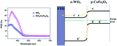
In this work, a p–n heterojunction film consisting of n-type WO3 and p-type CuFe2O4 was synthesized via two steps. The n-type WO3 film was deposited on the FTO substrate by a doctor-blade method and then modified with p-type CuFe2O4 nanoparticles by a deposition-annealing method. The composite film was characterized by X-ray powder diffraction, scanning electron microscopy, transmission electron microscopy, X-ray photoelectron spectroscopy and UV-vis diffuse reflectance spectroscopy, showing that the CuFe2O4 nanoparticles were deposited on the surface of WO3 film. Meanwhile, photoelectrochemical measurements were used to investigate the photoelectrochemical properties. A photocurrent of 0.75 mA cm−2 at 0.6 V (vs. Ag/AgCl) was achieved with CuFe2O4/WO3, resulting in a 2.68 fold increase compared to pristine WO3. The presence of a p–n heterojunction facilitates the separation of photoinduced electrons and holes, leading to more efficient charge transfer, resulting in a significant improvement in PEC performance.
Even though WO3 has these promising characteristics, further improving the photoelectrochemical performance is necessary in order to satisfy practical application requirements. Besides loading WO3 on the conductive substrates (FTO or ITO) is in favor of the reuse and recycle of photocatalyst, most of the researchers have focused on broadening the photoresponse region of semiconductor or improving the separation of the photo-generated electrons and holes.5–7 The main methods for achieving the goal have included noble metal deposition,8,9 metal or non-metal element doping,5,6,10,11 surface modification,12 or coupled with other semiconductors.13–18 Among them, coupled with other semiconductors, which can promote the separation of the photoinduced electron–hole pairs via the different position of valence and conduction band from each other, is an effective method to improve the efficiency of water splitting.
MFe2O4 (M = Cu, Zn, Co etc.), which is a high thermal stable material with effective catalytic activity, has been used extensively in photocatalysis and solar water-splitting.19–21 Since most of the ferrates are p-type semiconductors, some of them can couple with n-type semiconductors to form p–n heterojunction composite particles (CuFe2O4/CdS, CuFe2O4/SnO2, CuFe2O4/TiO2 and CaFe2O4/WO3).14,22–24 For example, Miyauchi et al. prepared CaFe2O4/WO3 composite powders by mechanically mixing n-type WO3 with p-type CaFe2O4 particles, and the composite photocatalyst showed better performance than WO3 on the photocatalytic decomposition of acetaldehyde.14 The enhanced photocatalysis activity can be ascribed to the separation of the photo-generated electron–hole pairs by their potential difference at the p–n heterojunction. Even though the powdered composite photocatalyst is a great candidate in photocatalysis, its application is limited due to the low recyclability. To cover the shortage, loading p-type ferrate on the surface of n-type semiconductor film is expected to be an efficient route. Even though several works on the photocatalysis or photoelectrochemical property of n-type semi-conductor with p-type semiconductor (ferrate,25,26 Cu2O,27–30 NiO,31 Si,32 CdTe33 and BiOI34 etc.) film have been reported, the n-type WO3 film loaded with ferrate is lack of attention. To the best of our knowledge, this is the first report to study the photoelectrochemical performance of WO3 film loaded with CuFe2O4 nanoparticles.
In this paper, we fabricated the CuFe2O4/WO3 p–n heterojunction film by doctor-blade method and deposition-annealing method. Meanwhile, the photoelectrochemical properties had been systematically characterized by several methods, including linear sweep voltammetry, electrochemical impedance spectroscopy (EIS), Mott–Schottky and incident photon to current conversion efficiency (IPCE).
A deposition-annealing method was used to synthesize the CuFe2O4 nanoparticles on the as-prepared WO3 film (1.5 cm × 1 cm). In detail, 0.060 g of Cu(CH3COO)2·H2O was dissolved into 10 mL of de-ionized (DI) water to form a transparent solution firstly (solution A). Then, 0.196 g of K3Fe(CN)6 was dissolved into another 30 mL of DI water to form a transparent solution (solution B). After the two solutions were stirred for 10 min in the ice bath, respectively, the solution A was added into the solution B drop by drop under vigorously stirred in the ice bath. After further stirred in the ice bath for another 1 h, the as-prepared WO3 film was put into the solution. The mixture was transferred into a refrigerator, keeping at 0–4 °C in a refrigerator for 2 h. Then the film was taken out and washed by dipping in the DI water for 30 seconds. After drying at 60 °C, the CuFe2O4/WO3 film was calcined at 500 °C for 1 h. For comparison, the pristine WO3 film and the mixed solution were also calcined to prepare pure WO3 and bare CuFe2O4, respectively.
The SEM images of the WO3 and CuFe2O4/WO3 films are presented in Fig. 2. In Fig. 2a and b, the top-view of SEM images exhibit that both samples are nanoporous network composed of spherical particles, which are agglomerate and interconnected with each other. As can be seen in the cross sectional images (Fig. 2c and d), the thickness of both WO3 and CuFe2O4/WO3 films are about 3.2 μm however, the layer of CuFe2O4 can not be found. It means that CuFe2O4 may compactly deposit on the surface of WO3 film. Furthermore, the energy dispersive X-ray (EDX) analyses were recorded as shown in the Fig. S2,† and Cu and Fe can be detected in the sample of CuFe2O4/WO3 (Fig. S2b†).
![]() | ||
Fig. 2 SEM images of the surface morphology of (a) WO3 and (b) CuFe2O4/WO3 films; cross-sectional micrographs of (c) WO3 and (d) CuFe2O4/WO3 films. |
To get more detailed information on the crystalline structure of the composite, the TEM images of CuFe2O4/WO3 at different magnifications are displayed in Fig. 3. The low resolution image (Fig. 3a) shows the particles are spheres that are highly agglomerated, and the size of the sphere is approximately 40 nm. It can also be seen that a smaller particle with irregular size adhere to the sphere. Fig. 3b displays the lattice fringes of the smaller particle and sphere. The interplanar distances observed in the smaller particle and the sphere are 0.254 and 0.365 nm, which correspond to the 311- and 200-planes of tetragonal CuFe2O4 and monoclinic WO3, respectively. It is proved that CuFe2O4 nanoparticles are attaching to the WO3 to form CuFe2O4/WO3 composite.
![]() | ||
Fig. 3 (a) Transmission electron micrographs and (b) high resolution TEM (HRTEM) image of CuFe2O4/WO3. |
The presence of CuFe2O4 on the surface of WO3 film was further confirmed by the XPS spectra (Fig. 4). In Fig. 4a, the survey spectrum of WO3 and CuFe2O4/WO3 indicates peaks of elements W and O. The carbon peak is attributed to adventitious hydrocarbon from the XPS instrument itself, which is not indicated in the figure. Fig. 3b shows the XPS spectrum of the tungsten core level (W 4f). The two peaks at 35.47 and 37.62 eV in the spectrum can be assigned to W 4f7/2 and W 4f5/2, respectively, which are consistent with the reported values.36 Fig. 4c and d show the high-resolution XPS spectra for Fe 2p and Cu 2p, respectively. From the Fe 2p spectrum, it was found that the peaks at 711.2 and 724.7 eV are from Fe 2p3/2 and Fe 2p1/2, and a accompanying satellite peak visible at binding energie of around 718.4 eV is indicative of the presence of Fe3+ cations.37 Two distinct and intense peaks were appeared for the Cu 2p spectrum, which are Cu 2p3/2 = 932.6 eV and Cu 2p1/2 = 952.4 eV (ΔBE = 19.8 eV).38 A satellite peak at about 942.0 eV can also be seen, which provides evidence for the presence of Cu2+.37 The ICP analysis was employed to determine the concentration of various metals (Cu, Fe and W), and [Cu]:
[Fe]
:
[W] value of 1.51
:
3.12
:
100 was estimated, so the ratio of p semiconductor to n semiconductor is about 1.51
:
100 in this system.
The UV-visible spectra of pure WO3 and CuFe2O4/WO3 films are presented in Fig. 5. The bare WO3 film absorbs light with wavelengths smaller than 455 nm, corresponding to 2.72 eV of band gap energy.39 The absorbance edge of CuFe2O4/WO3 is 463 nm, corresponding to 2.68 eV of band gap energy. The slightly shift of absorbance edge is probably due to the higher absorption coefficient of CuFe2O4 for visible light (Fig. S3†). To investigate the flat band potential (Vfb) of samples, Mott–Schottky plots were employed with a frequency of 500 Hz as shown in Fig. 6. The value of Vfb is approximately equal to the value of x-intercept, which are 0.08 and 0.19 V (vs. Ag/AgCl) for WO3 and CuFe2O4/WO3, respectively. It can be found that a positive shift of flat band potential, and a shift of the Fermi level to positive potential. It is because that CuFe2O4 is a p-type semiconductor with a negative slope, whose flat band potential is about 0.5 V (vs. Ag/AgCl) (Fig. S4†).31 Moreover, the potential of Fermi levels of WO3 and CuFe2O4 is in equilibrium after forming the p–n heterojunction.24 So the CuFe2O4/WO3 has a positive flat band potential compared with pure WO3 film.
To further study the effect of the valence band maximum (VBM) of the WO3 and CuFe2O4/WO3, the valence band X-ray photoelectron spectroscopy (VB XPS) was employed to determine the electronic structure. Fig. 7 indicates that the VBM of CuFe2O4/WO3 moves to higher potential compared with that of WO3. That is to say, the VBM of the WO3 changes after coupling with CuFe2O4, in agreement with the changing of flat band potential.
To investigate the photoresponsivity of the films, the photocurrent–potential was measured using a linear sweep voltammetry method as shown in Fig. 8. The current values of two samples are about zero under dark condition. In the range of 0.3–1.0 V (vs. Ag/AgCl), a significant improvement of photocurrent under irradiation indicates the enhanced PEC activity after loading of CuFe2O4. A photocurrent of 0.75 mA cm−2 (0.6 V vs. Ag/AgCl) was achieved with CuFe2O4/WO3, which is 1.68 times higher than that of bare WO3 (0.28 mA cm−2), the conversion efficiency is about 0.48% (Fig. S5†), and it is higher than the results reported in the similar system.35,40 For a semiconductor thin film photoanode, the magnitude of photocurrent is determined by the competition of photo-generated carriers migration and recombination.41 At the same time, most of the photogenerated electron/hole pairs recombine generating heat and/or light after excitation.42 In fact, p–n junction can greatly enhance the charge separation owing to the internal electric field.43 Hence, the p–n heterojunction formed by n-type WO3 and p-type CuFe2O4 has a beneficial effect on the separation of the photo-generated carriers and decreasing the recombination of electrons and holes. In addition, the onset potential of CuFe2O4/WO3 (Fig. S6†) shows a positive shift compared with pure WO3, which is consistent with the results of flat band potentials in Fig. 6a. To observe the effect of composition (ratio of p/n) on the photoelectrochemical performance, various composite films were fabricated by changing the concentration of Cu(CH3COO)2·H2O and K3Fe(CN)6 (the details in the ESI†), and the photocurrent curves are shown in Fig. S7.† It can be concluded that the ratio of p/n ≈ 1.51:
100 might be the optimized composition in our system. Transient photocurrent were also measured at 0.4 V (vs. Ag/AgCl) with chopped light, as shown in Fig. 6b. The photocurrent of both samples are about zero when the light is chopped, and the photocurrent show decay mode under irradiation, meaning that the recombination process occurs. The transient time constant (τtran) were calculated from the equation: exp(−t/τtran) = (It − If)/(Ii − If).44,45 It is 3.5 s for WO3 and 4.5 s for CuFe2O4/WO3, respectively, indicating the p–n heterojunction accelerates the separation of photoinduced electrons and holes. The stability of WO3 and CuFe2O4/WO3 were also investigated, as shown in Fig. S8.† After irradiation of 1140 s, the photocurrents of WO3 and CuFe2O4/WO3 decrease with 64.1% (from 0.100 to 0.036 mA cm−2) and 56.2% (from 0.442 to 0.194 mA cm−2), respectively. It means that the CuFe2O4/WO3 film shows a little better stability compared to the bare WO3 film.
![]() | ||
Fig. 8 (a) Linear sweep voltammograms of WO3 and CuFe2O4/WO3, (b) transient photocurrent of WO3 and CuFe2O4/WO3. |
EIS measurement was employed to study the electron transfer resistance across the electrode–electrolyte interfaces under visible irradiation. Fig. 9a shows the Nyquist plots which can be used to characterize the charge transfer resistance and the separation efficiency of the photo-generated electrons and holes.45 The impedance spectra, consisting of a semicircle, can be fitted with an appropriate equivalent circuit. As shown in Fig. 9b, the equivalent circuit includes a series resistance (Rs), a charge transfer resistance (Rct) and a constant phase element (CPE). The semicircle of CuFe2O4/WO3 is smaller than that of WO3, and the fitting results of Rs are 2479 and 364 ohm for WO3 and CuFe2O4/WO3, respectively. It means that the p–n heterojunction decrease the charge transfer resistance at the interface of electrode and electrolyte, leading to more efficient charge separation. Correspondingly, the characteristic frequency peaks for WO3 and CuFe2O4/WO3 in Bode phase plots are shown in Fig. 9c. The peak of CuFe2O4/WO3 shifts to low frequency from 53.5 Hz to 10.0 Hz compared with WO3. Therefore, the lifetime of photoelectrons (τ) for the films can be estimated by the equation: τ = 1/2πfmax,45 where fmax is the peak frequency, and the τ are 3.0 and 15.9 ms for WO3 and CuFe2O4/WO3, respectively. The presence of p–n heterojunction facilitates the separation of photoinduced electrons and holes, leading to prolongation of photoelectrons lifetime, resulting in a significant improvement in PEC performance.
![]() | ||
Fig. 9 EIS plots of the WO3 and CuFe2O4/WO3: (a) Nyquist plots, (b) equivalent circuit and (c) Bode plots, the inset of (a) is the full plot of WO3. |
In order to further explore the quantitative correlation of light absorption on the films, IPCE measurements were performed at the bias of 1.0 V (Fig. 10). The light response region of WO3 and CuFe2O4/WO3 are both at 310–475 nm. The CuFe2O4/WO3 film shows a higher IPCE value compared with WO3 film in the whole photoresponse region. Moreover, the maximum IPCE value of CuFe2O4/WO3 is 47.27% at 350 nm, which is 1.21 times higher than that of WO3. As the number of electrons in the external circuit produced by an incident photon at a given wavelength divided by the number of incident photons, IPCE is determined by three microscopic processes: light harvesting (LH), separation of opposing charges (CS), and a collection of the charges (CC) at the electrodes. Considering the similar light absorbance of two samples as shown in Fig. 5, the different value of IPCE at the whole light response region indicates that the separation of opposing charges is the main factor. So the improvement of photoelectrochemical performance is ascribed to the presence of p–n heterojunction.
Based on the above results, a simple mechanism of the conduction and valence band positions for CuFe2O4/WO3 is shown in Fig. 11. The space charge region caused by p–n heterojunction has a beneficial effect of improving the charges separation.22 In this way, photo-generated holes transfer to CuFe2O4, and more photo-generated electrons can transfer to conductive substrates without recombination. Therefore, it can be concluded that the p–n heterojunction promotes electron/hole separation, leading to an enhanced photoelectrochemical performance.
Footnote |
† Electronic supplementary information (ESI) available. See DOI: 10.1039/c5ra18279d |
This journal is © The Royal Society of Chemistry 2015 |