
Fabrication of three dimensional layered vertically aligned carbon nanotube structures and their potential applications
J. D. Beard*,
K. E. Evans and
O. R. Ghita
Exeter Advanced Technologies, College of Engineering, Mathematics and Physical Sciences, University of Exeter, Harrison Building, Exeter, EX4 4QF, UK. E-mail: j.beard@exeter.ac.uk
First published on 1st December 2015
Abstract
This paper proposes a new technique for fabrication of vertically aligned carbon nanotube (VACNT) structures, controlled in shape, height and functionality, through continuous successive growth of VACNT layers by chemical vapour deposition (CVD) combined with patterning strategies. This was achieved by vacuum deposition of additional catalyst material onto the original VACNT “forest” layer. A second forest layer is then observed to grow underneath the first by CVD. It is proposed that the new catalyst material diffuses through the porous nanotube forest to coat the growth substrate underneath. The enhanced height, coating, and vertical alignment of the nanotube forests were verified by electron microscope observation. By repeating this process, aligned nanotube bi-layers and tri-layers were grown, producing a “stack” of nanotube layers. By using a “shadow mask” patterning technique to screen areas of the original forest from catalyst deposition, the growth can be confined to specific areas of the substrate. Potentially, these multilayer nanotube structures would have diverse applications as long composite reinforcements, p–n junctions for electronic devices, or to allow the production of near net shape complex multilayer nanotube structures.
Introduction
Vertically aligned carbon nanotube clusters, described as “forests”, are desirable for a diverse range of applications, such as supercapacitor electrodes, sensing devices, thermoelectric devices and reinforcements in composite materials.1–4 Vertically-aligned forests are particularly desirable for composite reinforcement due to ideal parallel alignment of the nanotube fibres.5 These forests can be produced from catalyst-coated substrates using chemical vapour deposition (CVD) of hydrocarbon precursors such as methane or ethylene,6,7 up to heights of several millimetres.8,9In general, nanotube growth by CVD uses a thin film metal catalyst deposited on a substrate (e.g. silicon) and annealed at high temperatures (600–1000 °C) in a reducing atmosphere. The catalyst used is typically a vacuum-deposited metal film supported by an aluminium oxide (Al2O3) sublayer. When heated to the reaction temperature, the metal film is annealed to form isolated nanoparticles. The presence of the Al2O3 layer prevents migration of the catalyst metal into the silicon substrate, and provides an ideal surface for the nanoparticle formation. Introduction of hydrocarbon gas to the nanoparticle catalyst nucleates carbon at the nanoparticle growth sites, forming carbon nanotubes. The tube stiffness and mutual van der Waals attraction between adjacent tubes causes them to grow perpendicular to the growth substrate and form self-aligned forests, with strong parallel intertube alignment.6 Patterning of the catalyst layer using microfabrication techniques e.g. electron beam lithography or photolithography has previously been extensively demonstrated to localize the nanotube growth at chosen sites, creating a diverse range of nanotube structures with many applications.10 However, previously only single layers of nanotubes have been patterned in this way.
CNT forest height is limited by the catalyst's active lifetime, with the growth abruptly ceasing to leave a dense vertically-aligned forest of nanotubes of uniform height with a level upper surface. Much research aiming to enhance the forest height has focused on increasing the growth time or rate by careful control of reaction conditions,8 or the use of oxygen-donating substances such as water11 to remove amorphous carbon from the catalyst substrate, as the buildup of amorphous carbon is known to limit the catalyst effectiveness.12
This paper describes a novel approach to enhance the functionality and height of a nanotube forest by growing a second forest layer beneath the original forest, and demonstrates that the second-layer growth can also be localized and patterned by use of a shadow-mask technique. This was achieved by an additional catalyst deposition onto the pre-existing nanotube forest, followed by the fabrication of the second layer by CVD under similar conditions as were used to produce the first layer. It was expected initially that this new growth would occur on top of the original forest due to the deposited catalyst layer. However, electron microscope observation showed the formation of additional aligned nanotubes beneath the original layer. This surprising result can be explained in terms of diffusion of the catalyst material during vacuum deposition, with the material passing through the original porous nanotube forest to reach the silicon growth substrate.
Growth of such multilayer structures could have a wide range of applications, both due to the enhanced nanotube length, localization of growth, and the multilayer nature of the resulting forests. Multilayer nanotube structures could be used as p–n junctions in electronic devices, and patterned growth would allow the fabrication of complex devices. Patterning the nanotube layers could also be used as a route to produce three-dimensional CNT structures by additive manufacturing. These potential applications are illustrated diagrammatically in Fig. 1 and described in more detail in the Results & discussion section of this paper.
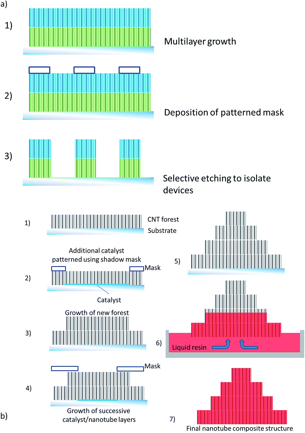 | ||
| Fig. 1 Potential applications of multilayer nanotube stacks. (a) Schematic of potential method of device fabrication. (1) Growth of nanotube multilayer with nanotube layers of different electronic properties (2) patterning of a shadow mask to expose specific regions of the layer by lithographic techniques (3) etching (e.g. by laser ablation) to remove nanotubes and isolate layered device structures. (b) Schematic of a potential additive layer manufacturing (ALM) process using layer-by-layer nanotube growth. (1) Deposition of initial nanotube layer (2) deposition of patterned catalyst in desired region (3) growth of new layers (4) further patterning and catalyst deposition to create successive layers (5) nanotube stack structure (6) infusion of liquid resin into structure by capillary flow (7) final composite structure. | ||
Experimental
Catalyst films of iron with an aluminium oxide supporting layer (2/25–45 nm thickness respectively) were deposited on clean silicon wafers with a 100 nm silicon dioxide surface layer by electron beam evaporation. Carbon nanotube growth was carried out by CVD using a SabreTube furnace (Absolute Nano) with external gas preheater8 and suspended silicon platform heater.13 Following flushing of the quartz tube with helium gas, substrates were annealed for 2 minutes in a helium/hydrogen atmosphere. Ethylene was then introduced as a carbon source for the growth of carbon nanotubes. The external preheater in this system allows pre-treatment of all reactant gases at 975–1050 °C, while the catalyst was annealed at a substrate temperature of ∼800 °C. A “cap” consisting of a single-side polished silicon wafer (0.525 mm thick) was placed with the unpolished side down on top of the catalyst substrate – the presence of the cap is known to moderate gas flow over the substrate surface and results in increased nanotube yield.14 This method is discussed in more detail in our previous papers.15 A schematic of the growth process is shown in Fig. 2a. | ||
| Fig. 2 (a) Schematic of the nanotube growth process by chemical vapour deposition (CVD). (b) Schematic of additional catalyst deposition and nanotube growth. (1) Catalyst is deposited by electron beam evaporation onto a silicon substrate (2) the first nanotube forest layer is grown by CVD (3) a new catalyst layer is deposited (4) an additional forest layer is grown beneath the pre-existing forest due to the diffusion of the re-deposited catalyst to the silicon substrate. | ||
The SabreTube system allows full optical observation of the sample during growth. The thickness of the CNT forest film can be monitored during growth using a laser rangefinder system, with the beam “spot” reflected from the silicon wafer cap (see Fig. 2a).
Following the growth of nanotubes, the samples were cleaved perpendicular to the plane of the growth substrate, creating identical control samples and samples for additional catalyst coating. The samples for coating were transferred back to the electron beam evaporator and an additional catalyst film (Al2O3/Fe with a nominal thickness of 15–25/1.5 nm respectively; in reality the thickness may vary due to a masking effect from diffusion through the nanotube forest) deposited onto the nanotube forest. In some cases, areas of the samples were masked during the second deposition process using glass cover slips to cover areas of the sample.
The nanotube forest was then returned to the SabreTube CVD system and the second nanotube film grown under the same conditions as for the first film, including the use of a silicon wafer cap. This process was repeated using the control samples. A schematic of this process is shown in Fig. 2b. For tri-layer sample growth, the catalyst deposition/CVD process was repeated with the bi-layer forests, depositing catalyst onto the forests and repeating the CVD growth.
For SEM observation, samples were cleaved again to allow imaging in cross-section and imaged using a Hitachi S3200N SEM-EDS system at a 20 kV accelerating voltage. EDS measurement was carried out using the SEM on partially-masked coated samples using the same accelerating voltage. Higher-magnification imaging was carried out using a field-emission SEM (FE-SEM) system (FEI Nova 600). For observation in cross-section, samples were mounted perpendicular to the SEM stage.
For TEM observation, small quantities of nanotubes were removed from the silicon substrates by hand using a scalpel blade and dispersed in ethanol in an ultrasonic bath. The resulting suspension was pipetted onto standard holey carbon TEM grids and allowed to dry overnight in ambient conditions. TEM imaging was carried out using a JEM-2100 LaB6 TEM system at 200 kV accelerating voltage. Nanotube diameters were measured using ImageJ software (v1.46r).
Raman spectroscopy was carried out using a Renishaw Raman microscope with a laser wavelength of 532 nm, at 1% of maximum power to avoid oxidation of the nanotubes. Each spectrum was an average of 5 scans of 10 s duration each.
Results & discussion
TEM imaging was carried out to examine the structure of individual nanotubes. Examples of TEM images of the as-grown uncoated nanotubes are shown in Fig. 3a and b; measurement of nanotube diameters showed them to have a mean diameter of 7.8 nm, with a standard deviation of 1.2 nm. A histogram of measured nanotube diameters is shown in Fig. 3c. Imaging at increased magnification showed the nanotubes to have a multiwall structure, as shown in Fig. 3b.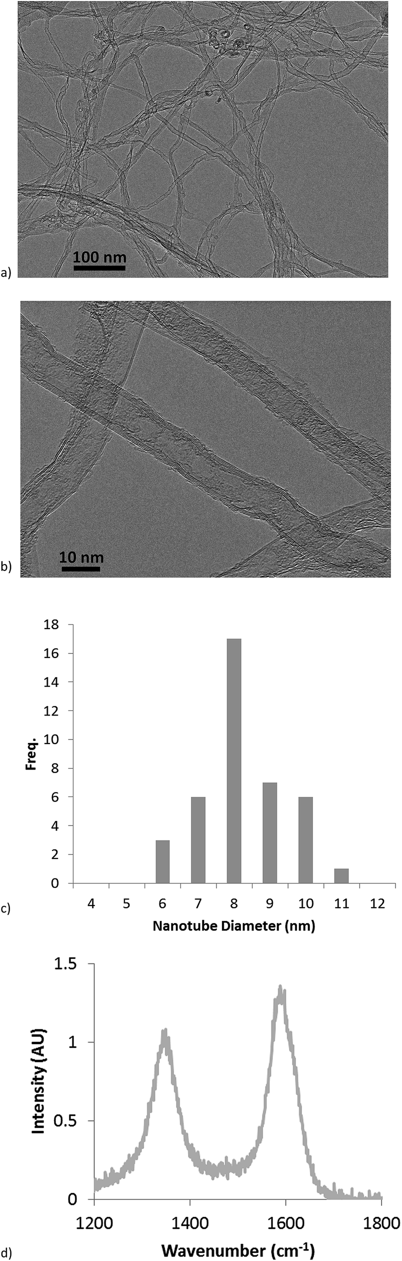 | ||
| Fig. 3 (a) TEM image of carbon nanotubes. (b) Image at higher magnification, showing multiwall structure. (c) Histogram of carbon nanotube diameters. (d) Raman spectrum (intensity normalised to D-band peak at 1300–1400 cm−1) recorded on as-grown nanotube forest, showing G- and D-bands. | ||
Raman spectroscopy measurements on the as-grown nanotube forests showed clear peaks in the range of 1300–1400 and ∼1600 cm−1, known as G- and D-bands. A typical spectrum is shown in Fig. 3d. The G-band is associated with the sp2-bonded carbon found in nanotubes, while the D-band is known to arise from the presence of amorphous carbon formed as an undesired by-product of the CVD process, and also from defects in the nanotubes. Therefore, the ratio of intensities (Ig/Id) of the G- and D-peaks is commonly used as an indication of nanotube quality. For the measured nanotube forests, Ig/Id = 1.2 ± 0.1, a similar value to that seen in the study by Meshot et al. for aligned nanotubes produced under similar CVD conditions.8 This indicates the presence of some defects and/or amorphous carbon in the nanotube forests; however, this could be overcome by refinement of the CVD reaction conditions (as also demonstrated in the study by Meshot et al.).
Fig. 4a shows SEM images and distribution of elements detected by EDS on the upper surfaces of the nanotube forests following the second catalyst deposition process and 2 minute annealing in He/H2. The alignment of the nanotubes is not clearly visible when viewed from the upper surface of the forest, due to the presence of a thin tangled layer at the forest top as commonly observed in vertically-aligned forests of nanotubes fabricated by CVD.16 A strong contrast between coated regions and those left uncoated due to masking was observed. The boundary between these regions is clearly visible by SEM, as seen in Fig. 4a. Imaging using SEM and FE-SEM showed increased diameter of the nanotubes in the coated regions compared to those in the uncoated areas due to the presence of the Al2O3/Fe coating, as shown in Fig. 4b–d. Energy-dispersive X-ray spectroscopy (EDS) mapping showed an increase in Al and O abundance in the coated region, as shown in Fig. 4a; the abundance of Fe may be too small to detect by EDS due to the extremely low thickness of the deposited Fe layer. These images and measurements confirmed the successful coating of the nanotubes. There was also a difference in colour between the coated and uncoated nanotubes visible using the unaided eye as shown in the photographs with enhanced brightness in Fig. 4e.
 | ||
| Fig. 4 (a) SEM image of carbon nanotube forest upper surface after re-deposition of catalyst and annealing (but no second layer growth). The Al2O3/Fe coating is visible on the nanotubes in the unmasked regions of the sample. EDS maps demonstrate increased abundance of Al and O in the coated regions. (b) SEM images at higher magnification showing carbon nanotubes in forest top surface. Nanotubes in the coated region show increased diameters due to the presence of coating. (c) and (d) FE-SEM images of nanotubes in uncoated (c) and coated (d) regions. Note that these images present the upper surface of the aligned nanotube forests, which shows a tangled appearance, as opposed to the strongly aligned nanotubes visible when imaged from the side of the forest (see Fig. 5–7). The nanotube diameter is again seen to increase in the coated regions. (e) Photographs of coated CNT forest, masked so that the central portion of the CNTs was coated. Upon enhancement of the image brightness, the coated region can be seen as a brighter band. | ||
The coated samples were measured to increase in thickness by 0.1–0.4 mm during the second CVD growth phase using the laser rangefinder system (see Fig. 2a). Observation by scanning electron microscope (SEM) of samples which were cleaved for imaging in cross-section showed the presence of the additional forest layer, and also allowed the observation of parallel filaments in the side walls of the forests, indicating that all the forest layers consist of vertically aligned nanotubes. An example of a bilayer forest is shown in Fig. 5a. The boundary between forest layers is clearly visible by SEM, as shown in Fig. 5b. The control samples displayed no new nanotube growth after identical CVD growth processes; an example is shown in Fig. 5c. This illustrates that the new growth is attributable to the re-deposition of the Fe/Al2O3 catalyst.
 | ||
| Fig. 5 (a) SEM image showing side view of sample with an additional catalyst layer post-growth, after cleaving the sample to allow imaging in cross-section. The nanotube bilayer is visible. (b) Image of interlayer boundary, showing nanotube alignment. (c) Control sample with no addition catalyst layer, which does not demonstrate the bilayer structure. | ||
Samples with masked areas showed growth of additional nanotubes within the unmasked regions (as shown in Fig. 6a), while no additional growth was observed in the masked regions away from the masked/unmasked region boundaries (as shown in Fig. 6b). This result demonstrates that the deposition of the second and subsequent layers can be patterned using a shadow mask to localise the catalyst and nanotube growth at specific sites on the substrate. Growth of single-layered patterned nanotube forests has been widely demonstrated;14 this result shows that patterning techniques can also be applied to multilayer growth, which could open up a wide range of potential applications (see below; see also Fig. 1).
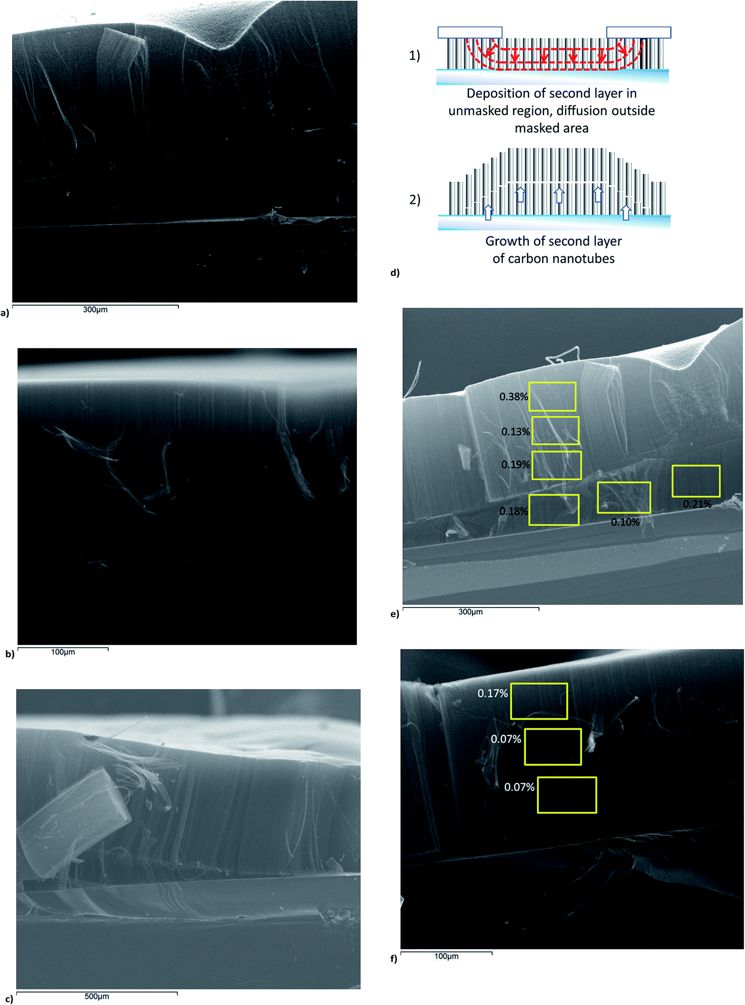 | ||
| Fig. 6 Cross-sectional SEM images showing restriction of nanotube growth away from coated regions of the substrate on a sample. (a) In coated regions, two layers are visible. (b) In masked, uncoated areas away from the masked/unmasked boundary, only one layer of nanotubes is visible. (c) Tail-off of CNT height close to boundary in masked region. (d) Schematic representation of diffusion into boundary of unmasked region, and resulting nanotube growth. (e) EDS mapping images showing abundance of aluminium from Al2O3 coating in upper and lower layers in coated region. (f) Distribution of aluminium in masked region, showing comparatively lower abundance. | ||
At the boundary between masked and unmasked regions, a region in which the second layer increased smoothly in thickness was observed, from zero thickness (no second layer growth) in the masked region to 0.2–0.3 mm in the unmasked region. Nanotube growth close to the boundaries between masked and unmasked areas is shown in Fig. 6c. As discussed in more detail below, the formation of new nanotube layers is due to diffusion of Al2O3/Fe catalyst through the original forest layer to reach the substrate, allowing the initiation of additional nanotube growth. This variation in height may be due to diffusion of the catalyst a short distance into the unmasked areas through the inter-nanotube gaps in the nanotube forest, creating an area of sparser catalyst density extending into the unmasked regions, and so causing reduced nanotube growth in this region. This effect is illustrated diagrammatically in Fig. 6d.
EDS measurements were also carried out on cross-sectional views of the nanotube forest. These measurements showed that aluminium was more abundant in the top layer of the CNT forest bilayer in the coated area, and furthermore increased abundance was seen towards the top of the CNT forest. This further supports diffusion of the Al2O3 catalyst into the forest during the second catalyst deposition, as the diffusion process would result in a decreasing concentration of Al2O3 further from the forest top. In the uncoated areas, the concentration of aluminium observed is lower, and close to the detection threshold of the EDS system (∼0.1%). Abundance of aluminium in these different regions is shown in Fig. 6e and f.
The patterning of the nanotube growth in the second layer illustrates that the additional growth is not due to catalyst re-activation, where the annealing process and introduction of additional carbonaceous gas causes the original catalyst film to produce additional CNT growth. Such catalyst re-use has been reported after mechanical removal of nanotubes from growth substrates,17 where it was reported that nanotube yield decreases with each re-use of the catalyst. However, in the case of the patterned samples nanotube growth is not observed within the masked regions away from the boundaries of the unmasked regions, indicating that the catalyst in these areas did not re-activate and the growth of additional CNT layers is due to the re-deposition of catalyst rather than to catalyst re-activation.
Imaging of the samples which had undergone three catalyst deposition/CVD stages showed the presence of three separate layers of nanotubes, as shown in Fig. 7a. During growth, the thickness of each layer was measured using the laser rangefinder system. This allows the layer associated with a given growth stage to be identified. For example, in the sample shown in Fig. 7, the layers were measured at three different thicknesses when grown. The thickest layer was grown last, and when imaged by SEM was observed to have formed underneath the previous, thinner layers. This illustrates, together with the results from samples with masked and unmasked regions, that the nanotube growth occurs from beneath the original forest, displacing the original forest upwards.
 | ||
| Fig. 7 (a) Growth of a sample with three layers. Measurement of the different layer thicknesses during growth shows that the thickest, bottom layer is deposited last, indicating that the growth occurs from the substrate beneath the original forests. (b) Carbon nanotubes in successive layers imaged at high magnification. The nanotubes become increasingly tangled in successively lower layers. | ||
The growth of new nanotube layers beneath the original layer can be explained as follows. Nanotube growth occurs due the formation of iron nanoparticles during the annealing of the Al2O3/Fe catalyst layers. Upon introduction of hydrocarbon precursor gas, each nanoparticle nucleates carbon decomposed from the precursor gas, acting as a “seed” for the growth of a carbon nanotube. The nanotube forests which demonstrated additional growth were subjected to a second vacuum deposition of Al2O3/Fe catalyst after growth of the original nanotube layer. Carbon nanotubes are known to occupy only 1–2% of the volume of nanotube forests produced by CVD; the remainder is empty space.18,19 Most of the surface of the growth substrate beneath the original forest layer thus remains unoccupied by the nanotubes. It is likely, therefore, that during the vacuum deposition process additional catalyst material is able to diffuse through the forest layer(s) and coat the substrate even through the original nanotube forest. Upon re-annealing of the catalyst, this new catalyst layer forms new nanoparticle seeds, which re-initiate the growth of nanotubes upon introduction of carbonaceous gas and lead to the creation of new nanotubes. The growth of this layer displaces the original nanotube layer upwards forming a new aligned layer below the original forest.
Imaging at higher magnification showed different morphologies in the individual nanotubes, with lower layers appearing more “tangled” and disordered, with increased waviness of the nanotubes (see Fig. 7b). This can potentially be attributed to a masking effect by the nanotube forest, which reduces the amount of catalyst which diffuses to the substrate and so decreases the surface density of catalyst nanoparticles. This results in a reduced density of nanotubes in the forest, allowing greater space for nanotube growth away from the forests' vertical axis and producing a more disordered forest.
It was also considered whether the increased disorder of the nanotubes was due to the weight of the pre-existing layers above the new layer, which could cause buckling and tangling of the nanotubes below. However, the growing nanotubes in the first and subsequent layers are able to push against the weight of the silicon “cap”, which is used to moderate gas flow during CVD, without buckling or loss of parallel alignment. Previous studies have shown that CVD grown nanotubes are each able to exert approximately 0.16 nN of force during growth, at least 104 times the nanotube's own weight; acting together, the combined force from the nanotubes in the forest are easily able to displace the silicon cap.20 Since the density of the cap is much greater than that of the highly porous nanotube forest, its weight is much larger and each new forest layer does not add significantly to the weight above the next layer. For this reason, the increased tangling observed in the lower layers is unlikely to be due to the weight of the nanotube layers above each new layer.
Previous studies in successive growth of VACNT layers concentrated on the re-activation of the catalyst by etching methods that remove the amorphous carbon “cap” that inhibits the nanotube growth.21,22 However this method has principally been used to produce only short CNT growth, for example to interrupt and restart nanotube growth to allow measurement of the growth rate at different stages during the CVD growth.22 Other studies have shown that nanotubes can be used as growth scaffolds for further nanostructures, for example for the growth of ZnO nanowires.23
The growth of multilayer aligned nanotube forests demonstrated here potentially allows for a large range of applications. Adaptation of this method could allow for the layer-by-layer fabrication of complex nanotube structures. The electronic properties of nanotubes vary depending on their composition, doping and structure. For example, adventitious oxygen-doping causes single-walled nanotubes to behave as p-type semiconductors in air;24 they can be converted to n-type by surface modification with organic monolayers,25 or doped by addition of other elements during the CVD process, in a similar manner to silicon doping for semiconductor applications.26
In addition, the properties of nanotube forests, such as the diameter of nanotubes and whether the nanotubes are single-walled or multi-walled, is known to depend on both the CVD growth conditions and the catalyst composition. Therefore by deposition of different catalysts, it is possible that this technique could be used to deposit nanotube layers with different properties in each layer.27,28
There has been significant past research in the fabrication of p–n and transistor junctions between nanotubes of different electronic characteristics29 or between nanotubes and other materials.30–33 By varying the properties of nanotubes in individual layers, layer-by-layer fabrication of CNT forests by CVD would allow intertube junction fabrication to be carried out on a wafer scale, and so would be scalable to current mass production methods for electronic chips.34–37 This would also have the advantage of not requiring additional nanotube film transfer steps. Nanotube forests can be patterned and selectively etched post-production by laser ablation using lithographically patterned masks,38 or, more commonly, patterned by localisation of the catalyst at specific sites on the substrate using lithography methods.7 In this study we have shown that patterning techniques using shadow masks can also be used to localise the second (and probably also subsequent) layers at desired sites (see Fig. 6). This would potentially allow nanotube-based circuits or other devices (such as thermoelectric junctions) to be fabricated in the same manner as current silicon chips. p–n junctions represent a key element in the manufacturing process of semiconductor devices, solar cells and LEDs, therefore these developments could impact on these industries. A proposed route for this process is illustrated in Fig. 1a.
Functionalization of nanotube forests has also been used for other applications. For example, fluorination of the nanotube sidewall can be used to provide a basis for attachment of further functional groups, e.g. specific biomolecules for biosensing applications.39 Another approach is to attach functional groups such as carboxylic acid groups to the nanotube ends as anchoring sites for other molecules.40 The growth of a layer-by-layer forest structure would potentially allow for each layer to be functionalised differently, increasing the versatility of functionalised nanotubes for novel applications. A limitation of this method is that functionalization in one layer would need to be preserved during the high temperatures required for CVD of the second layer; however CVD production of carbon nanotubes has recently been demonstrated at lower temperatures (∼400 °C) and so this limitation may be avoided by this technique.41 The high stability of fluorine–carbon bonds also means this type of functionalization should survive CVD of additional layers, allowing selective addition of other functional groups onto the fluorinated layers post-CVD.
In addition, there is the potential for enhancement of nanotube forest height. Repeating the catalyst deposition and CVD processes would allow the growth of multi-layers of CNTs up to arbitrary forest heights and in well-defined forms to fabricate specific structures. Due to their high aspect ratio and the high tensile strength of nanotubes, these stacked CNTs would be ideal for reinforcement of composite materials3,5 or for cold spinning of CNT fibres.42
A further potential application would be the construction of three-dimensional structures in an additive manufacturing or 3D-printing method by patterning successive stacked nanotube layers. This would allow the fabrication of complex three-dimensional structures composed of nanotubes. Infusion of polymer resin into the nanotubes by capillary action could then be applied to fabricate a near net shape aligned nanotube composite structure. This proposed application is shown schematically in Fig. 1b.
Conclusions
We have been able to enhance the height of a pre-existing CVD-grown carbon nanotube forest, and develop multilayered patterned CNT forest structures, by deposition of an additional Al2O3/Fe catalyst, allowing the growth of an additional nanotube forest beneath the original nanotube layer. Observation by electron microscope verified the presence of the additional layer as well as the parallel alignment of the carbon nanotubes. This process was shown to be also able to produce tri-layer samples, and in theory could be applied to produce nanotube “stacks” with an arbitrary number of layers. In addition, we were able to localize the growth at selected sites by masking the surface of the nanotube forest during the second catalyst deposition stage.We conclude that this extra growth arises from diffusion of the Fe catalyst through the pre-existing nanotube forest layer to the substrate during the deposition of the layer by electron beam evaporation, where it is able to form a new catalyst layer and initiate the growth of a new nanotube layer during CVD.
The resulting stacked forests would have numerous applications. This layer-by-layer fabrication technique is similar to the deposition processes used in the fabrication of integrated circuits and could potentially allow for fabrication of nanotube-based electronic devices on a wafer scale. In addition, the enhancement of the aligned nanotube forest height would allow for increased reinforcement effectiveness in polymer composites and nanotube fibres. Layer-by-layer patterning of the forest layers would also allow the additive manufacture of large-scale aligned nanotube structures, creating a new method for the fabrication of three dimensional nanotube architectures.
The CVD process is highly scalable and adaptable to production on an industrial scale, with the capacity for complex process control (e.g. using the in situ optical film thickness monitoring used in this and other studies8). There is also potential for combination with other methods of catalyst deposition, such as inkjet printing, which has been shown to be suitable for deposition of nanoparticle catalysts for the production of high quality aligned nanotube forests.15
Acknowledgements
The authors would like to thank Dr Lesley Wears, Mr Tom Loughran, Ms Ke Bao, and Dr Hong Chang of the University of Exeter for their assistance in our electron microscopy imaging, and Dr Anna Lewandowska for assistance in Raman spectroscopy.Notes and references
- B. Kim, H. Chung and W. Kim, Nanotechnology, 2012, 23, 155401 CrossRef PubMed.
- Y. Wang and J. Yeow, J. Sens., 2009, 2009, 493904 Search PubMed.
- R. Allen, O. Ghita, B. Farmer, M. Beard and K. Evans, Compos. Sci. Technol., 2013, 77, 1–7 CrossRef CAS.
- X. Li, H. Gao, W. Scrivens, D. Fei, X. Xu, M. Sutton, A. Reynolds and M. Myrick, Nanotechnology, 2004, 15, 1416 CrossRef CAS.
- E. Garcia, A. Hart, B. Wardle and A. Slocum, Adv. Mater., 2007, 19, 2151–2156 CrossRef CAS.
- M. Jose-Yacaman, M. Miki-Yoshida, L. Rendon and J. Santiesteban, Appl. Phys. Lett., 1993, 62, 202–204 CrossRef CAS.
- A. Hart and A. Slocum, J. Phys. Chem. B, 2006, 110, 8250–8257 CrossRef CAS PubMed.
- E. Meshot, D. Plata, S. Tawfick, Y. Zhang, E. A. Verploegen and A. J. Hart, ACS Nano, 2009, 3, 2477–2486 CrossRef CAS PubMed.
- K. Hata, D. Futaba, K. Mizuno, T. Namai, M. Yumuru and S. Iijima, Science, 2004, 306, 1362–1364 CrossRef.
- H. Chen, A. Roy, J.-B. Baek, L. Zhu, J. Qu and L. Dai, Mater. Sci. Eng., R, 2010, 70, 63–91 CrossRef.
- K. Hata, D. Futaba, K. Mizuno, T. Namai, M. Yumura and S. Iijima, Science, 2004, 306, 1362–1364 CrossRef CAS PubMed.
- S. Pattinson, K. Prehn, I. Kinloch, D. Eder, K. Koziol, K. Schulte and A. Windle, RSC Adv., 2012, 2, 2909–2913 RSC.
- L. van Laake, A. Hart and A. Slocum, Rev. Sci. Instrum., 2007, 78, 083901 CrossRef PubMed.
- A. Hart and A. Slocum, J. Phys. Chem. B, 2006, 110, 8250–8257 CrossRef CAS PubMed.
- J. Beard, J. Stringer, O. Ghita and P. Smith, ACS Appl. Mater. Interfaces, 2013, 5, 9785–9790 CAS.
- E. R. Meshot, E. Verploegen, M. Bedewy, S. Tawick, A. R. Woll, K. S. Green, M. Hromalik, L. J. KKoerner, H. T. Philipp, M. W. Tate, S. M. Gruner and A. J. Hart, ACS Nano, 2012, 6, 5091–5101 CrossRef CAS PubMed.
- E. Polsen, S. Tawfick, E. Meshot, and A. Hart, presented at 38th North American Manufacturing Research Conference (NAMRC38), Kingston, Ontario, 2010 Search PubMed.
- R. Allen, O. Ghita, B. Farmer, M. Beard and K. Evans, Compos. Sci. Technol., 2013, 77, 1–7 CrossRef CAS.
- B. Wardle, D. Saito, E. Garcia, A. Hart, R. de Villoria and E. Verploegen, Adv. Mater., 2008, 20, 2707–2714 CrossRef CAS PubMed.
- A. Hart and A. Slocum, Nano Lett., 2006, 6, 1254–1260 CrossRef CAS PubMed.
- J. AuBuchon, L.-H. Chen and S. Jin, J. Phys. Chem. B, 2005, 109, 6044–6048 CrossRef CAS PubMed.
- L. Zhu, J. Xu, F. Xiao, H. Jiang, D. Hess and C. Wong, Carbon, 2007, 45, 344–348 CrossRef CAS.
- W.-D. Zhang, Nanotechnology, 2006, 17, 1036–1040 CrossRef CAS PubMed.
- P. Collins, K. Bradley, M. Ishigami and A. Zettl, Science, 2000, 287, 1801–1804 CrossRef CAS.
- M. Shim, A. Javey, N. Kam and H. Dai, J. Am. Chem. Soc., 2001, 123, 11512–11513 CrossRef CAS PubMed.
- Y. Jin, W. Hsu, Y. Zhu, P. Watts, Y. L. Chueh, L. Chou, H. Kroto and D. Walton, AIP Conf. Proc., 2004, 723, 53 CrossRef CAS.
- R. Xiang, E. Erik Einarsson, Y. Murakami, J. Shiomi, S. Chiashi, Z. Tang and S. Maruyama, ACS Nano, 2012, 6, 7472–7479 CrossRef CAS PubMed.
- Y. Murakami, S. Chiashi, Y. Miyauchi and M. Hu, Chem. Phys. Lett., 2004, 385, 298–303 CrossRef CAS.
- X. He, X. Wang, S. Nanot, K. Cong, Q. Jiang, A. Kane, J. Goldsmith, R. Hauge, F. Leonard and J. Kono, ACS Nano, 2013, 7, 7271–7277 CrossRef CAS PubMed.
- Y. Jung, X. Li, N. Rajan, A. Taylor and M. Reed, Nano Lett., 2013, 13, 95–99 CrossRef CAS PubMed.
- J. Lee, P. Gipp and C. Heller, Appl. Phys. Lett., 2004, 85, 145–147 CrossRef CAS.
- C. Hewitt, A. Kaiser, S. Roth, M. Craps, R. Czerw and D. Carroll, Nano Lett., 2012, 12, 1307–1310 CrossRef CAS PubMed.
- Q. Cao, H.-S. Kim, N. Pimparkar, J. Kulkarni, C. Wang, M. Shim, K. Roy, M. Alam and J. Rogers, Nature, 2008, 454, 495–500 CrossRef CAS PubMed.
- R. G. de Villoria, A. J. Hart and B. L. Wardle, ACS Nano, 2011, 6, 4850–4857 CrossRef PubMed.
- S. S. Meysami, F. Dillon, A. A. Koós, Z. Aslam and N. Grobert, Carbon, 2013, 58, 151–158 CrossRef CAS.
- S. S. Meysami, A. A. Koós, F. Dillon and N. Grobert, Carbon, 2013, 58, 159–169 CrossRef CAS.
- S. S. Meysami, A. A. Koós, F. Dillon, M. Dutta and N. Grobert, Carbon, 2015, 88, 148–156 CrossRef CAS.
- F. Cheong, K. Lim, C. Sow, J. Lin and C. Ong, Nanotechnology, 2003, 14, 433–437 CrossRef CAS.
- E. Hooijdonk, C. Bittencourt, R. Snyders and J.-F. Colomer, Beilstein J. Nanotechnol., 2013, 4, 129–152 CrossRef PubMed.
- S. Baker, P. Colavita, K.-Y. Tse and R. Hamers, Chem. Mater., 2006, 18, 4415 CrossRef CAS.
- N. Na, Y.-G. So, Y. Ikuhara and S. Noda, IEICE Tech. Rep., 2014, vol. 113, pp. 35–38.
- Y.-L. Li, I. Kinloch and A. Windle, Science, 2004, 304, 276–278 CrossRef CAS PubMed.
| This journal is © The Royal Society of Chemistry 2015 |