
Physicochemical interface effect in Cu2O–ZnO heterojunction on photocurrent spectrum
Kiryung Eoma,
Seunghwan Kimb,
Dongyoon Leeb and
Hyungtak Seo*a
aDepartment of Energy Systems Research, Department of Materials Science & Engineering, Ajou University, Suwon 443-739, Republic of Korea. E-mail: hseo@ajou.ac.kr
bGyeonggi Science High School, Suwon 440-800, Republic of Korea
First published on 19th November 2015
Abstract
This study reports the effect of oxide heterojunction solar cell (HSC) arrangement on the solar photocurrent spectra and the physical correlation to the interfacial band electronic structure. Based on the p-Cu2O/n-ZnO oxide junction, two types of stack arrangements were prepared to observe the solar photocurrent spectral change: FTO/Cu2O/ZnO/Al and FTO/ZnO/Cu2O/Al structures. In the photovoltaic cell structure, FTO was utilized as the p-type electrode, Cu2O as the p-type semiconductor, ZnO for the n-type semiconductor and Al as the n-type electrode. The HSC characteristics were characterized using ultraviolet-visible spectroscopy, X-ray photoelectron spectroscopy (XPS), diode current–voltage measurements, and finally, incident photon-to-current efficiency (IPCE). As a result, the IPCE spectra of the HSC were largely affected by (1) the bandgap of the first layer semiconductor, which is the first layer receiving incidence light regardless of the bandgap energy, and (2) the interfacial electronic band offset values in each stack. Therefore, this result offers a possible mechanism for why the HSC consisting of the FTO/Cu2O/ZnO stack shows better IPCE response than the FTO/ZnO/Cu2O stack in the view of electronic band-alignment.
1. Introduction
Research on oxide heterojunction solar cells (HSCs), consisting of a p–n junction with different bandgap oxide layers, has been actively performed due to their cost-effectiveness, facile manufacturing process control, and reliable material properties. These merits place the oxide HSC as a potential future solar cell, which can offer technical solutions to meet the current requirements in the commercial solar cell industry, such as low raw material prices, low manufacturing costs, and easy mass-production processes. Nevertheless, the power conversion efficiency (PCE) of oxide HSCs is much lower than that of Si and chalcogenide thin film solar cells. Although the merit of oxide HSCs is related to the abundance of metal oxide species such as Cu-oxide and Zn-oxide, the best PCE levels of oxide HSCs have been reported only at 1–5% unless rare-earth p- or n-type metal oxides are used.1 Therefore, research activities on oxide HSCs are mainly focused on the improvement of the PCE level.2,3 Among the many oxides considered as the absorber layer, Cu2O is highlighted as a p-type semiconductor with a bandgap of 2.1 eV and a PCE level that is theoretically expected to reach up to 17%. Since Cu2O is non-toxic, naturally abundant, and can be fabricated and processed at low cost, its application to light emitting diodes, gas sensors, and p-type absorber materials in solar cells is being studied.4–7In conventional homo-junction solar cells like Si p–n junction cells, the interfacial properties are well predicted and modelled, so that they come with easily controllable design factors.8–10 However, for oxide HSCs, the interface is the most challenging part due to the significant chemical mixing of elements, non-stoichiometry, and defect/trap-site generation. In view of solar cell operation, this gives rise to a large uncertainty about the interfacial band offset, which determines the effective carrier separation at the junction. Although theoretical predictions were made on the band-alignment model based on a previous report, the degree of precision based on such predicted models is not so high at all in the case of oxide HSCs.11 This raises the need for experimental approaches to investigate the interfacial physicochemical properties using appropriate spectroscopic techniques.
In this study, we investigated the effect of the interfacial properties on the photon energy dependent PCE in p-Cu2O/n-ZnO HSCs by changing the stack arrangement. In a typical thin film HSC cell, there is a top window layer comprising a large bandgap n-type semiconductor and an absorber layer with a small bandgap p-type semiconductor at the bottom. However, we noticed a significant solar photocurrent spectral change in the incident photon-to-current efficiency (IPCE) when the stacking order was reversed compared to that in a conventional cell. In order to investigate this, focusing on the interfacial chemical properties and band-alignments in both p/n and metal–semiconductor junctions, ultraviolet-visible (UV-vis) spectroscopic and X-ray photoelectron spectroscopic (XPS) measurements were carried out. This result provides a valuable guideline for Cu2O-based oxide HSC structure optimization based on the electronic band-alignment.
2. Experimental
A 0.7–4 μm thick p-type cupric oxide layer, Cu2O was fabricated on fluorine doped tin oxide (FTO) glass using an electrodeposition method, applying −3 V of bias at 60 °C in a pH 9 solution consisting of 0.2 M copper sulfate (>99.9%, Sigma Aldrich) and 3 M lactic acid (88–92%, Sigma Aldrich) for 40 min.12–15 The 120 nm thick n-type ZnO layer was deposited using RF magnetron sputtering under the conditions of preheating for 10 min, pre-sputter for 5 min, 300 °C, and 1.00 × 10⁻² Torr under Ar 10 sccm flow. In addition, for the fabrication of the reverse layer, ZnO was deposited under vacuum on FTO followed by Cu2O which was applied to minimize the subcutaneous oxidation of Cu2O due to high temperature ZnO sputtering. For the p–n junction, an Al electrode with a thickness of 50 nm and a diameter of 100 μm was deposited using electron-beam deposition.The diode I–V characteristics were evaluated using a Keithley 2612 current–voltage (I–V) source meter. The photocurrent spectra, as a function of the wavelength (from 1200 to 300 nm) of monochromatic incident light generated by a xenon lamp onto the Al electrode in the HSC, were measured to achieve the IPCE results. A standard Si solar cell (BS-500, BUNKOUKEIKI Co., Japan) was utilized to calculate the IPCE. The crystal structures were analyzed using X-ray diffraction (XRD, UltimaIII, Rigaku, Japan) and the surface chemical binding state, valence band-edge state, and depth-profile were obtained by X-ray photoelectron spectroscopy (XPS, theta probe base system, Thermo Fisher Scientific Co., USA). The bandgap of each layer was determined using a UV-vis spectrometer (Cary 5000, Agilent, USA).
3. Results and discussion
The crystallinity of Cu2O (at a thickness of 4.2 μm, 1.9 μm, and 720 nm) on FTO (at a thickness of 250 nm) glass as a function of thickness was evaluated using XRD at diffraction angles from 20 to 50° and an angle interval of 0.02° (Fig. 1(a)). The XRD data reveals diffraction peaks for Cu2O corresponding to the cubic structure (JCPDS-01-071-3645, a = 0.42685 nm) having (110), (111) and (200) planes at diffraction angles of 29.66°, 36.54° and 42.33° respectively. The 1.9 μm thick sample shows the strongest XRD peaks among the samples, even stronger than the thickest (4.2 μm) sample, indicating that the crystallinity does not correlate with the thickness of the film deposited using vacuum deposition. Based on the XRD peak intensity, the preferential crystal plane of Cu2O is also changed from (200) for the 720 nm and 1.9 μm thick films to (111) for the 4.2 μm thick film. Upon fabrication of the diodes, the best diode results were obtained with the 720 nm thick Cu2O film while diodes with other Cu2O films exhibited poor performance (not shown here). This indicates that the bulk crystallinity of the Cu2O films is not a deciding factor, but only a partial effect in controlling the diode characteristics. Instead, we propose that the interface of Cu2O/ZnO is more relevant to the diode properties. The SEM data in Fig. 1(b) and (c) reveal the cross-sectional morphology of the FTO/ZnO/Cu2O and FTO/Cu2O/ZnO stacks respectively. In order to distinguish each layer easily, the target thickness of each layer was set to 200 nm for ZnO and 500 nm for Cu2O. However, the interface formation leads to variation in the resulting thickness as seen in the SEM images. Each layer was formed as a continuous film and energy dispersive spectroscopic analysis on specific spots identified distinctive Cu and Zn concentrations in the CuO and ZnO layers respectively as shown in the atomic% plots of Fig. 1(b) and (c). | ||
| Fig. 1 (a) XRD patterns of Cu2O layers with different thicknesses (red: 720 nm, black: 1.9 μm, blue: 4.2 μm) and SEM images (left) and atomic fraction graphs (right) extracted from EDS spot analyses at each layer (spectrum 1–3) of (b) FTO/ZnO/Cu2O and (c) FTO/Cu2O/ZnO stacks. In the XRD pattern, reference diffraction peaks from a JCPDS card are also shown. | ||
UV-vis spectroscopic analysis was performed to achieve the optical bandgap to be used for the electronic band structure model by measuring absorbance and transmission data (Fig. 2). In Fig. 2(a) and (b), Cu2O has a high absorbance at 300–500 nm, corresponding to UV and the visible range and this confirms that Cu2O has a clear advantage for absorbing the incident light and producing photo-carriers in the visible range. In Fig. 2(c) and (d), ZnO reveals a strong absorbance at <400 nm and a high transparency at >80% in the visible range, which makes ZnO an ideal material for the window layer of solar cells. The optical bandgap from the UV-vis absorbance data was extracted using the Tauc plot shown in Fig. 3. Tauc plot curves were plotted for different values of n (n = 1/2, in the case of direct bandgap) and α (the absorption coefficient calculated from absorption spectra and photon energy).16 The direct bandgaps of Cu2O and ZnO were 1.4 and 3.2 eV respectively.17–19 However, the typical Cu2O optical bandgap is ∼2.1 eV and this bandgap difference is related to the formation of CuO at the electrodeposited Cu2O surface, which rapidly occurs in ambient air. Indeed, the absorbance data in Fig. 2(a) shows the marked absorbance in the wavelength down to 1100 nm, which is due to light absorption in the surface CuO subphase.20 The effect of the stack arrangement of Cu2O and ZnO layers on the optical properties was investigated by UV-vis analysis shown in Fig. 4. The stack of FTO/Cu2O/ZnO/Al shows a lower absorbance in the range of 600–1000 nm than that of the reverse stack arrangement (FTO/ZnO/Cu2O/Al), but no difference in the range of 300–500 nm is observed, which is the high absorbance band. Therefore, it is deduced from Fig. 4 that the stacking arrangement has an outstanding impact on the degree of CuO phase formation on the Cu2O surface, leading to absorbance at 500–1100 nm but having no effect on the strong absorption region due to the ZnO and Cu2O phases.
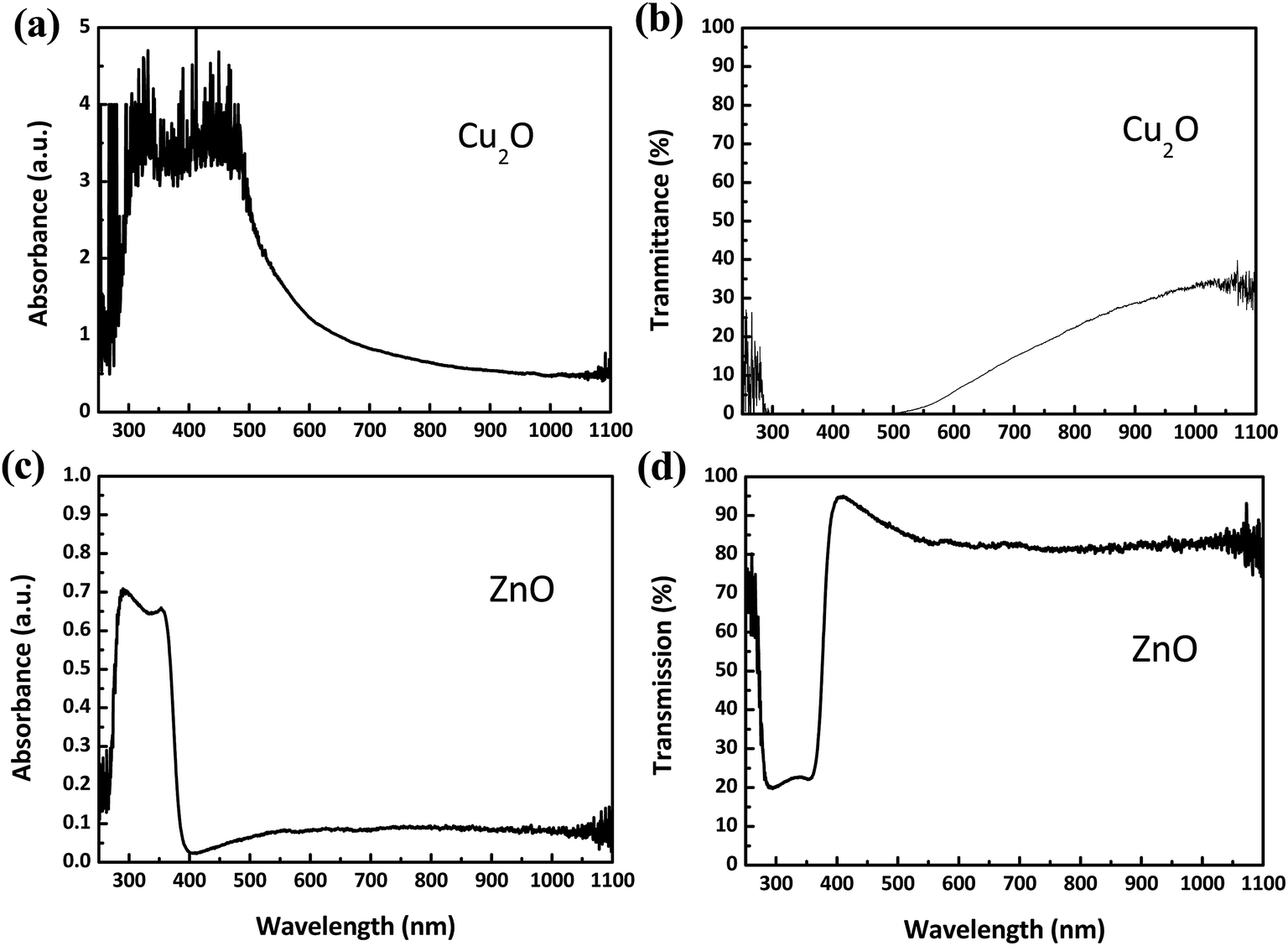 | ||
| Fig. 2 UV-vis absorbance and transmittance spectra: (a) absorbance and (b) transmittance of Cu2O, (c) absorbance and (d) transmittance of ZnO. | ||
 | ||
| Fig. 3 The extracted optical bandgap of (a) Cu2O and (b) ZnO from the Tauc plot. | ||
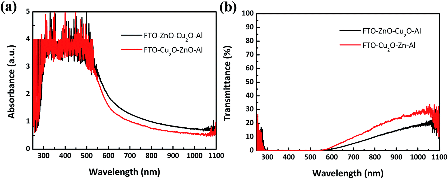 | ||
| Fig. 4 (a) Absorbance and (b) transmittance spectra of the whole stacks of FTO/ZnO/Cu2O/Al and FTO/Cu2O/ZnO/Al. | ||
The I–V results in Fig. 5 show the p/n diode characteristics of differently stacked oxide junctions. Both junctions reveal regular diode properties with asymmetric I–V behavior with bias polarity. However, the bias polarity using a forward current is different depending on the junction type; −bias for the ZnO/Cu2O (n/p) junction (Fig. 5(a)) and +bias for the Cu2O/ZnO (p/n) junction (Fig. 5(b)). It is noted that the diode rectification of ZnO/Cu2O is inferior to that of Cu2O/ZnO since the CuO subphase formed on Cu2O generates additional energy barriers for charge transport.21,22 Under the dark-current condition, the rectification factor of each diode at ±5 V is 2 for the ZnO/Cu2O stack and 30 for the Cu2O/ZnO stack. The photo-current is clearly observed in both diodes upon light exposure, and notably, the ratio of photo-current/dark-current for Cu2O/ZnO is >∼103, offering a good visible photo-response performance. The repeated I–V curves with 10 cyclic sweeps and time-dependent transient photo-current traces under a continuous bias of 2 V are shown in Fig. 5(c) and (d) for each stack. It turns out that the Cu2O/ZnO stack has an outstanding dark-current baseline drift compared to ZnO/Cu2O, (1) without a noticeable change in the net photo-current level and (2) showing no residual lag in the time-dependent photo-current transition. This suggests that the FTO/Cu2O/ZnO stack has a high number of non-photoactive charge trap sites, which are considered to be intrinsically formed at the FTO/Cu2O interface, which is different compared to the FTO/ZnO interface in the FTO/ZnO/Cu2O stack.
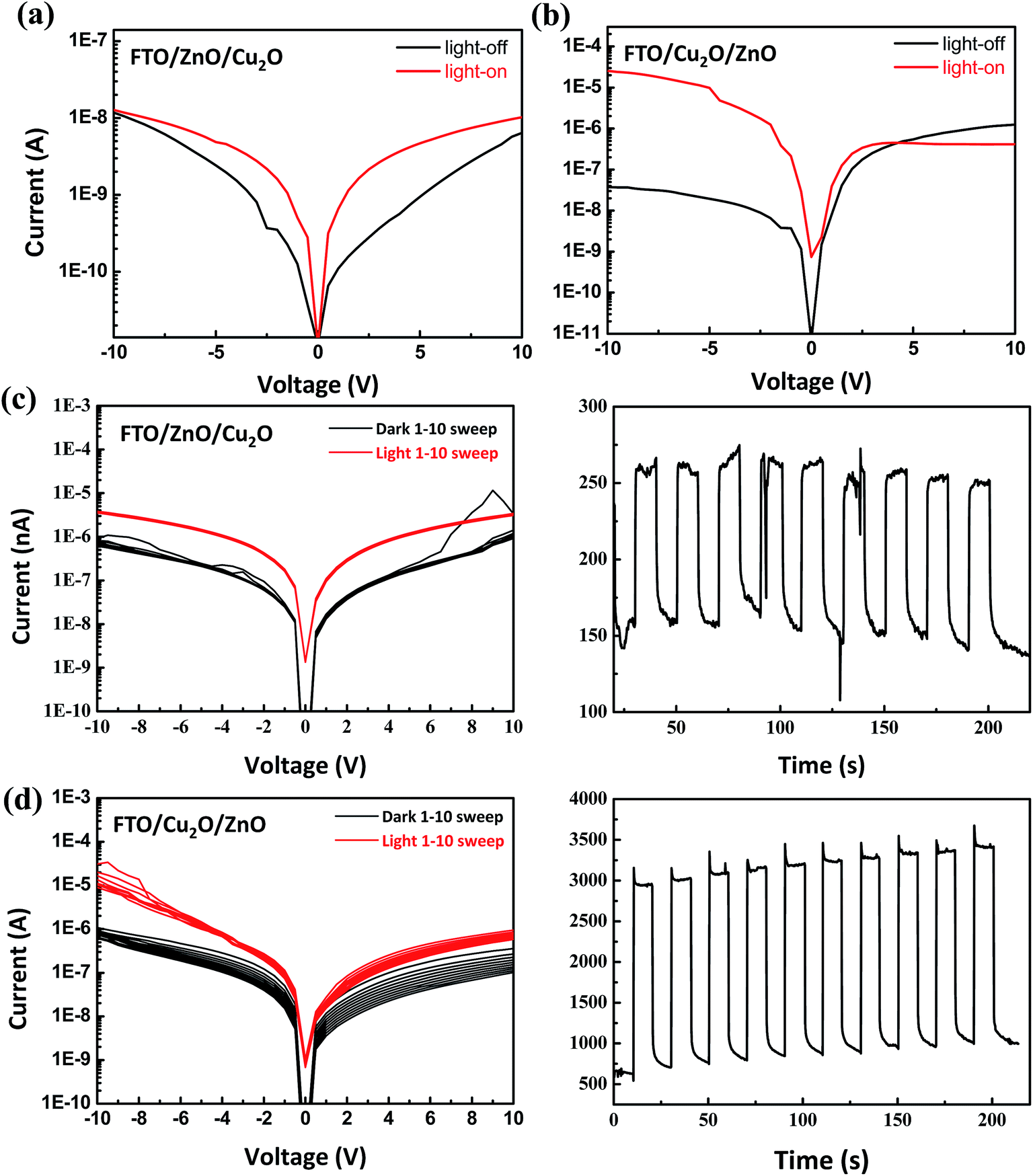 | ||
| Fig. 5 I–V characteristics of (a) FTO/ZnO/Cu2O/Al and (b) FTO/Cu2O/ZnO/Al under light-off (dark-current) and light-on (photo-current) conditions. The repeated I–V (left) and I–t curves (right) of (c) FTO/ZnO/Cu2O/Al and (d) FTO/Cu2O/ZnO/Al. | ||
Fig. 6 shows IPCE spectra to investigate the spectral response of the photocurrent with changing the stack arrangement. In the IPCE spectrum for the Cu2O/ZnO junction, three distinctive photo-current bands are observed at <400, 400–600, and 900–1200 nm of wavelength. Based on the optical absorption data in Fig. 4, each band corresponds to the photo-carrier generation in ZnO (<400 nm) and Cu2O (400–600, 900–1200 nm). However, the ZnO/Cu2O junction shows an overall low IPCE spectrum except in the wavelength range of 1000–1200 nm, in spite of the fact that the optical absorption in ZnO/Cu2O is almost same as that of Cu2O/ZnO and its optical absorption in the long wavelength range at 1000–1200 nm is even higher than that of the Cu2O/ZnO junction. The relatively high IPCE at 1000–1200 nm in the ZnO/Cu2O junction is presumed to be due to the CuO subphase, the bandgap of which is 1036 nm or 1.2 eV.15,21,22 The lower IPCE in the ZnO/Cu2O junction compared to the Cu2O/ZnO junction over most of the wavelength range indicates that the electronic band alignment affected by the CuO subphase on Cu2O plays a crucial role in IPCE. Therefore, XPS analysis was performed to evaluate the band alignment structure of each junction. PCEs of the Cu2O/ZnO HSC are reported to be 0.1–3%.2,3,14,23 The PCE level of the Cu2O/ZnO HSC in this study is ∼0.1%, requiring more optimization. Nevertheless, an IPCE reaching 25% in the wavelength range of 800–1200 nm has not been reported in other works,1,3,24 so that can be considered to compensate for the low PCE level in the long wavelength range.
 | ||
| Fig. 6 IPCE spectra of (red) FTO/ZnO/Cu2O/Al and (black) FTO/Cu2O/ZnO/Al. | ||
Fig. 7(a) and (b) represent the XPS depth profiles (atomic elemental percent as a function of Ar sputtering time) for (1) FTO/Cu2O and (2) Cu2O/ZnO respectively. For sample (1), the FTO–Cu2O interfacial band alignment and CuO band structures are determined and for sample (2), the Cu2O/ZnO interfacial band alignment is obtained. The Ar sputtering condition was 0.2 nm s−1 (referenced to SiO2) and the sputtering raster area was 1 mm2. In Fig. 7(a) for FTO/Cu2O, the position at a sputter time (or etch time) of 0 s corresponds to the Cu2O top surface and a sputter time of 150 s corresponds to FTO with a reduction of the atomic percentage of Cu-2p. In Fig. 7(b) for Cu2O/ZnO, the position at a sputter time of 0 s corresponds to the ZnO top surface with a high atomic percentage of Zn-2p, 300–400 s is the interfacial region, and >500 corresponds to Cu2O with a rapid increase in the atomic percentage of Cu-2p. From the XPS depth profile, the elemental information along the depth position was identified and Cu-2p binding states were analyzed at specific points at the surface and bulk of each sample. As shown in Fig. 7(c), at the Cu2O top surface in sample 1 (0 s of sputter time), CuO (933.4 eV) and Cu(OH)2 (934.7 eV) binding states are resolved and satellite peaks of CuO (Cu(2+)) appear at 943.8 and 941.3 eV. This bond character clearly indicates that the Cu2O surface in sample 1 has a CuO subphase. In the bulk region of sample 1 (150 s of sputter time), only the Cu2O binding state (932.6 eV) is resolved without the CuO subphase features (Fig. 7(c)). On the other hand, sample 2 revealed only the Cu2O binding state (932.6 eV) in both the surface and bulk regions without any CuO-associated binding states or satellite peaks (Fig. 7(d)). This confirms the formation of a subcutaneous CuO-free Cu2O/ZnO interface in sample 2 due to the deposition of ZnO under vacuum onto CuO in the sputtering chamber without air exposure.
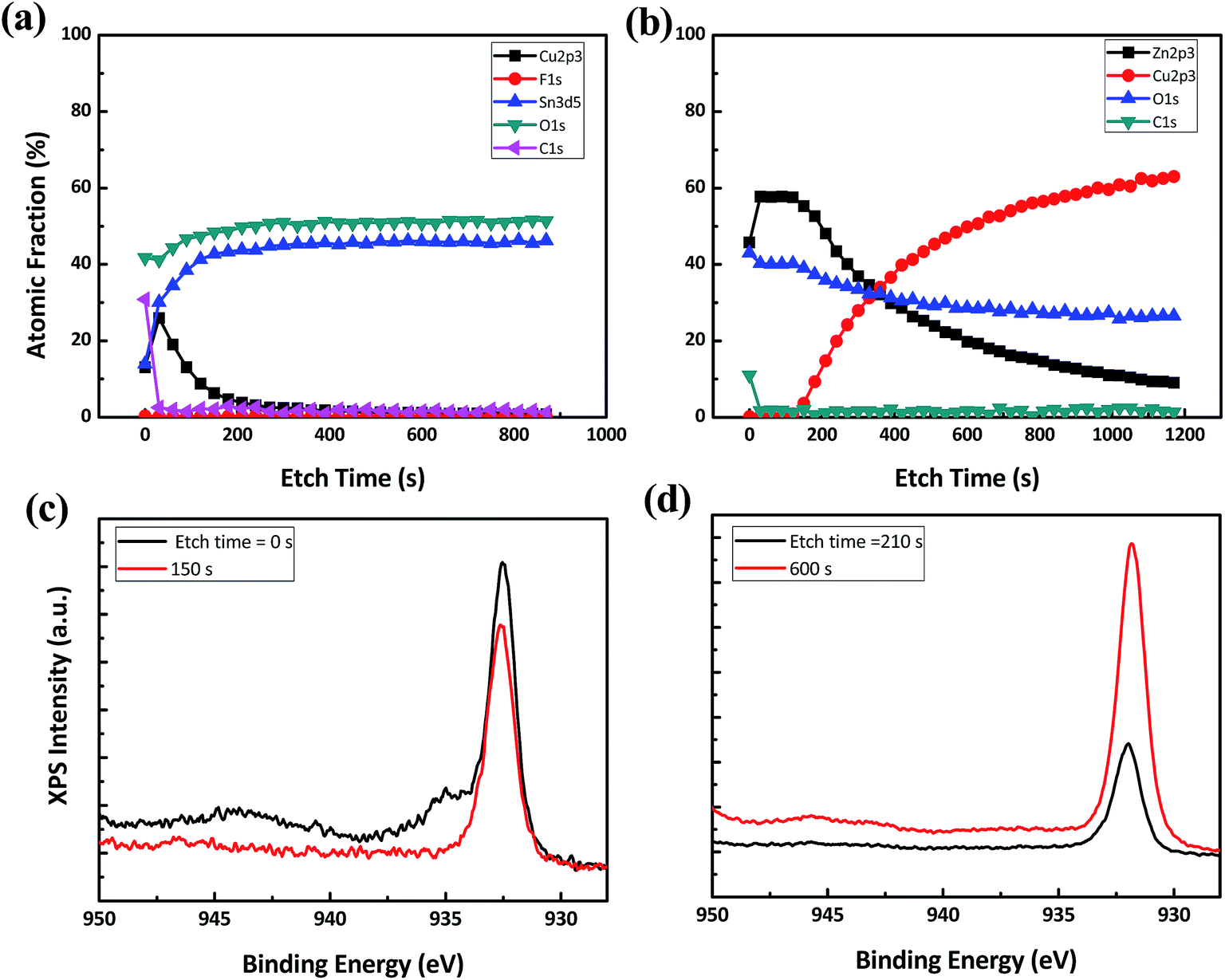 | ||
| Fig. 7 XPS depth profile of (a) FTO/Cu2O atomic %, (b) ZnO/Cu2O atomic % and Cu-2p narrow scan in the surface and bulk in (c) FTO/Cu2O (etch time at 0 s for the surface and 150 s for the bulk) and (d) ZnO/Cu2O (etch time at 210 s for the surface and 600 s for the bulk). | ||
At a specific point of the sample, the valence band maximum (VBM) as referenced to the Fermi energy level (EF) was extracted by inspecting the onset energy of the valence band edge XPS spectra. VBMs at the ZnO bulk (30 s of sputter time in Fig. 7(b)) and at the Cu2O bulk (1170 s of sputter time) are 1.75 eV (Fig. 8(a)) and 0.18 eV (Fig. 8(b)) respectively. Using a similar experimental approach combined with the optical bandgap data in Fig. 3 and the reference data for metal work functions and electron affinities,25–29 band alignments containing the conduction band offset (CBO) and valence band offset (VBO) as referenced to the EF level are calculated for FTO/ZnO, FTO/Cu2O, CuO/Al and ZnO/Al interfaces to construct the band alignment model in Fig. 8(c) and (d) for the FTO/Cu2O/ZnO/Al (i.e., stack 1) and FTO/ZnO/Cu2O/Al (i.e., stack 2) arrangements respectively. First, when the semiconductor work function is larger than the metal electrodes at the interface of the electrodes and the semiconductor junctions such as FTO/ZnO and Al/Cu2O, calculation of the barrier height (Vo) of the Schottky diode is done using eqn (1).30,31 This gives the Schottky barrier at each interface (0.04 eV at the interface between FTO/Cu2O, 1.6 eV at Al/ZnO, 0.59 eV at Al/CuO).
| Φs − Φm = Vo(Φm < Φs) | (1) |
 | ||
| Fig. 8 Valence band-edge XPS spectra with VBM values for (a) ZnO (at 30 s of etch time) for and (b) Cu2O (at 1170 s of etch time) in the FTO/Cu2O/ZnO stack. The electronic band structure and alignment of the (c) FTO/Cu2O/ZnO/Al and (d) FTO/ZnO/Cu2O/Al stacks. In the FTO/Cu2O/ZnO stack, there is no marked CBO and VBO to inhibit the charge separation at each interface. However, in the FTO/ZnO/Cu2O stack, hole transport toward FTO is blocked by the large VBO at ZnO/Cu2O and the CuO subphase present at the Cu2O surface leads to significantly different electronic band alignment from that in FTO/Cu2O/ZnO. | ||
Also, from the theory introduced by Kraut,32 the VBO (ΔEv) can be calculated using eqn (2) and (3) as following:
| ΔEv = EBVB − EAVB + [(EACL − EA/BCL) + (EB/ACL − EBCL)] | (2) |
| ΔEc = EBg − EAg + ΔEv | (3) |
4. Conclusions
This article reports the spectral changes in the solar photocurrent upon altering the arrangement of the Cu2O and ZnO layers in oxide HSCs. Based on XPS analysis, the top surface of Cu2O has a subcutaneous CuO subphase layer upon ambient air exposure in the case of FTO/ZnO/Cu2O arrangement, which diminishes the light absorption in Cu2O because of the high light absorption in the small bandgap (1.4 eV) subcutaneous CuO surface layer. As a result, the FTO/ZnO/Cu2O/Al HSC stack has a much lower IPCE over the entire wavelength range than the FTO/Cu2O/ZnO/Al stack. The band-alignment analysis, combining VB-edge XPS spectra (for VBM), UV-vis data (for optical bandgap), and reported work function and electron affinity values, yields the full electronic band-structure and alignment for each stack. From this, the first layer receiving incident light is the most important for the solar photocurrent spectra since it directly affects the IPCE by altering the dominant light absorption features in the stack and the VBO and CBO in the band electronic structure for charge transport. The CuO subphase in the ZnO/Cu2O stack is negative in all these respects but the CuO/ZnO stack has a clear advantage in band-alignment with no CBO and very small VBO values. This study therefore highlights the importance of band-alignment characterization to clarify the photo-current mechanism in oxide HSCs based on experimental analysis for efficiency optimization.Acknowledgements
This work was supported by the National Research Foundation (NRF), the Basic Science Program (NRF-2015R1A2A2A01003790 and NRF-2009-0094046) and by the C1 Gas Refinery Program (2015M3D3A1A01064899) funded by the Ministry of Education and the Ministry of Science, ICT, and Future Planning, Republic of Korea. K. Uhm and S. Kim and equally contributed to this work.References
- Y. Ievskaya, R. L. Z. Hoye, A. Sadhanala, K. P. Musselman and J. L. MacManus-Driscoll, Sol. Energy Mater. Sol. Cells, 2015, 135, 43–48 CrossRef CAS.
- A. Mittiga, E. Salza, F. Sarto, M. Tucci and R. Vasanthi, Appl. Phys. Lett., 2006, 88, 163502 CrossRef CAS.
- K. P. Musselman, A. Wisnet, D. C. Iza, H. C. Hesse, C. Scheu, J. L. MacManus-Driscoll and L. Schmidt-Mende, Adv. Mater., 2010, 22, E254–E258 CrossRef CAS PubMed.
- Y. Y. Kim, C. H. An, H. K. Cho, J. H. Kim, H. S. Lee, E. S. Jung and H. S. Kim, Thin Solid Films, 2008, 516, 5602–5606 CrossRef CAS.
- C. Malerba, F. Biccari, C. Leonor Azanza Ricardo, M. D′Incau, P. Scardi and A. Mittiga, Sol. Energy Mater. Sol. Cells, 2011, 95, 2848–2854 CrossRef.
- K. Matsuzaki, K. Nomura, H. Yanagi, T. Kamiya, M. Hirano and H. Hosono, Appl. Phys. Lett., 2008, 93, 202107 CrossRef.
- S. T. Shishiyanu, T. S. Shishiyanu and O. I. Lupan, Sens. Actuators, B, 2006, 113, 468–476 CrossRef CAS.
- L. Y. Isseroff and E. A. Carter, Chem. Mater., 2013, 25, 253–265 CrossRef CAS.
- L. Papadimitriou, C. A. Dimitriadis and L. Dozsa, Solid-State Electron., 1988, 31, 1477–1482 CrossRef CAS.
- O. Lupan, S. Shishiyanu, V. Ursaki, H. Khallaf, L. Chow, T. Shishiyanu, V. Sontea, E. Monaico and S. Railean, Sol. Energy Mater. Sol. Cells, 2009, 93, 1417–1422 CrossRef CAS.
- S. Calnan, Coatings, 2014, 4, 162 CrossRef.
- V. Georgieva and M. Ristov, Sol. Energy Mater. Sol. Cells, 2002, 73, 67–73 CrossRef.
- W. Septina, S. Ikeda, M. A. Khan, T. Hirai, T. Harada, M. Matsumura and L. M. Peter, Electrochim. Acta, 2011, 56, 4882–4888 CrossRef CAS.
- S. W. Lee, Y. S. Lee, J. Heo, S. C. Siah, D. Chua, R. E. Brandt, S. B. Kim, J. P. Mailoa, T. Buonassisi and R. G. Gordon, Adv. Energy Mater., 2014, 4, 1301916 Search PubMed.
- P. E. de Jongh, D. Vanmaekelbergh and J. J. Kelly, Chem. Mater., 1999, 11, 3512–3517 CrossRef CAS.
- Y. Nakano, S. Saeki and T. Morikawa, Appl. Phys. Lett., 2009, 94, 22111 CrossRef.
- Y. Nakano, S. Saeki and T. Morikawa, Appl. Phys. Lett., 2009, 94, 022111 CrossRef.
- J. Mass, P. Bhattacharya and R. S. Katiyar, J. Mater. Sci. Eng. B, 2003, 103, 9–15 CrossRef.
- G. Kaur, A. Mitra and K. L. Yadav, Prog. Nat. Sci., 2015, 25, 12–21 CrossRef.
- B. Kramm, A. Laufer, D. Reppin, A. Kronenberger, P. Hering, A. Polity and B. K. Meyer, Appl. Phys. Lett., 2012, 100, 094102 CrossRef.
- S. S. Wilson, J. P. Bosco, Y. Tolstova, D. O. Scanlon, G. W. Watson and H. A. Atwater, Energy Environ. Sci., 2014, 7, 3606–3610 CAS.
- R. E. Brandt, M. Young, H. H. Park, A. Dameron, D. Chua, Y. S. Lee, G. Teeter, R. G. Gordon and T. Buonassisi, Appl. Phys. Lett., 2014, 105, 263901 CrossRef.
- I. Masanobu, S. Tsutomu, M. Ko-Taro, I. Yuya, I. Minoru and T. Akimasa, J. Phys. D: Appl. Phys., 2007, 40, 3326 CrossRef.
- A. S. Zoolfakar, R. A. Rani, A. J. Morfa, S. Balendhran, A. P. O’Mullane, S. Zhuiykov and K. Kalantar-zadeh, J. Mater. Chem., 2012, 22, 21767–21775 RSC.
- I. Mora-Sero, L. Bertoluzzi, V. Gonzalez-Pedro, S. Gimenez, F. Fabregat-Santiago, K. W. Kemp, E. H. Sargent and J. Bisquert, Nat. Commun., 2013, 4, 2839 Search PubMed.
- M. Uda, A. Nakamura, T. Yamamoto and Y. Fujimoto, J. Electron Spectrosc. Relat. Phenom., 1998, 88, 643–648 CrossRef.
- A. Zainelabdin, S. Zaman, G. Amin, O. Nur and M. Willander, Appl. Phys. A: Mater. Sci. Process., 2012, 108, 921–928 CrossRef CAS.
- A. Mittiga, F. Biccari and C. Malerba, Thin Solid Films, 2009, 517, 2469–2472 CrossRef CAS.
- K. Jacobi, G. Zwicker and A. Gutmann, Surf. Sci., 1984, 141, 109–125 CrossRef CAS.
- A. M. Cowley and S. M. Sze, J. Appl. Phys., 1965, 36, 3212–3220 CrossRef CAS.
- W. Mönch, Surf. Sci., 1994, 299, 928–944 CrossRef.
- E. Kraut, R. Grant, J. Waldrop and S. Kowalczyk, Phys. Rev. B: Condens. Matter Mater. Phys., 1983, 28, 1965 CrossRef CAS.
- W. Wei, Z. Qin, S. Fan, Z. Li, K. Shi, Q. Zhu and G. Zhang, Nanoscale Res. Lett., 2012, 7, 1–5 CrossRef PubMed.
- T. D. Veal, P. King, S. Hatfield, L. R. Bailey, C. F. McConville, B. Martel, J. Moreno, E. Frayssinet, F. Semond and J. Zúñiga-Pérez, Appl. Phys. Lett., 2008, 93, 202108 CrossRef.
| This journal is © The Royal Society of Chemistry 2015 |