c-Si solar cells and Si n-MOSFETs prepared by ICP assisted hot wire implantation doping

Yi-Hao Chena, Shoou-Jinn Changa, Cheng-Liang Hsub, Yao-Kun Wub and Ting-Jen Hsueh*c
aInstitute of Microelectronics & Department of Electrical Engineering, Center for Micro/Nano Science and Technology, Advanced Optoelectronic Technology Center, National Cheng Kung University, Tainan 701, Taiwan, Republic of China
bDepartment of Electrical Engineering, National University of Tainan, Tainan 700, Taiwan, Republic of China
cNational Nano Device Laboratories, Tainan 741, Taiwan, Republic of China. E-mail: tj.hsueh@gmail.com

Received 27th August 2015 , Accepted 3rd November 2015

First published on 6th November 2015


Abstract

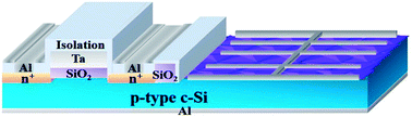
In this work, ICP-assisted hot wire implantation doping was carried out to fabricate c-Si solar cells. The obtained junction depth obtained was around 70 nm and the carrier concentration of the phosphorus was approximately 9.34 × 1020 cm−3. The efficiency of the fabricated SiNx/textured c-Si photovoltaic device was 16.08%. ICP-assisted hot wire implantation doping was also utilized to prepare Si n-MOSFETs. Experimental results indicate that the sub-threshold slope and on-off current ratio of the Si n-MOSFETs were about 0.39 V decade−1 and over 104, respectively.


Introduction

Various types of solar cells, such as silicon-based (crystalline, amorphous, and microcrystalline),1 GaAs,2 organic,3 and copper indium gallium selenide (CIGS)4 cells, have recently been developed. Among all solar cells, the crystalline silicon (c-Si) solar cell is the most widely used and has the largest global market share. In recent years, extensive research into high-performance and low-cost crystalline silicon solar cells has been performed.5 A c-Si solar cell has an anti-reflective coating (ARC) layer, an emitter layer, a p-base layer, and a metal contact layer.6 These layers have different chemical and physical properties. The formation of the p–n junction formation is one of the most critical steps in the fabrication of a solar cell. A solar cells also depends on the formation of a uniformly doped, emitter layer with low a sheet resistance.

Recently, many various doping methods were studied except the conventional fabrication. For example, Singh et al. used the solid phosphorous source (a 2′′ ceramic wafer that contains phosphorous pentoxide) to fabricate ∼13% c-Si solar cell.7 Other group has reported that using a thin film of phosphorus doped spin on dopant (SOD) technique to fabricate 15.6% c-Si solar cell.8 Lee et al. proposed ion implanted method and achieved an efficiency of 18.77%.9 In addition, the ion implantation technique which uses high energy ion beam to implant dopant into Si wafer has been widely used in IC industry. However, there are some problems for ion implantation such as crystallographic damage, damage recovery, amorphization, ion channeling, and high voltage safety. Ion implantation uses point or thread ion beam to fabricate semiconductor device on a Si wafer. Therefore, it is difficult to process a large area (such as LCD) and an entire batch. The equipment mainly included ion source, pre-acceleration, mass spectrometer, acceleration and magnets lenses so it is more expansive. However, for the produce of the solar cell, how to decrease cost is very important.

HWCVD only need an ion source, and it is easy to process a large area and an entire batch. It's easy to integrate with the in-line and the multi-chamber process, for example, ULVAC Corp. provided a prototype apparatus for mass-production of solar cells.10 As a result, the cost is cheaper. This work develops an ICP-assisted hot wire implantation doping (IHWID) technique for fabricating c-Si solar cells. The proposed method is simple, cost-effective, and suitable for mass production. With the growth of the internet of things (IoTs), self-powered11 devices are becoming more extensively investigated the IHWID technique can also be used to fabricate n-type MOSFETs (n-MOSFETs) for integration into c-Si solar cells. This work discusses the doping of Si-based devices.

Experiment

Fig. 1 schematically depicts the fabrication of pyramid-like structured c-Si photovoltaic devices and related processing steps. Prior to the fabrication of pyramid-like structured c-Si photovoltaic devices, 2.5 cm × 2.5 cm samples were cut from a (100)-oriented p-type silicon wafer with ρ = 1–10 Ω cm and a thickness of 200 μm. All samples were cleaned using a standard wet cleaning process. Subsequently, NaOH and IPA were diluted and used to etch isotropically the silicon wafer to form a surface with a pyramid texture, as shown in Fig. 2. The 100 nm thick SiO2 barrier layer was deposited on Si back surface via plasma-enhanced chemical vapor deposition (PECVD). The p–n junction was formed by phosphorus implantation with an ICP-assisted hot wire CVD system. In the phosphorus implantation process, the ICP power, filament temperature, substrate temperature, PH3 flow rate, Ar flow rate, distance between the hot wire filament and the substrate, and chamber pressure were 75 W, 1800 °C, 200 °C, 2 sccm, 20 sccm, 3.5 cm, and 50 mTorr, respectively. The sample was then placed into an RTA system and annealed at 900 °C for 3 min. A SiO2 film was etched is by wet etch (buffered oxide etch, BOE). Next, DC sputtering was used to deposit Al (2 μm) onto the back of the Si substrates and then annealed at 450 °C for 30 min to form an Al–Si back surface field (BSF) alloy layer on the backside. A 0.1 μm/2 μm thick Ag/Al layer was deposited on the front of the substrate to form an ohmic contact. Then, a metal mask was carefully put onto the Ag/Al layer to preserve the bus line. Finally, an 80 nm thick SiNx layer was deposited by ICPCVD on the surface of the device as an anti-reflection and isolation layer. The surface morphology was characterized using a JEOL JSM-6700F field emission scanning electron microscope that was operated at 10 keV. The junction depth (Xj) was obtained by from transmission electron microscopy (TEM). The crystal defects in the substrate were studied using Raman spectroscopy. The electrical characteristics of the n-MOSFET were measured using a Keithley 4200 semiconductor parameter analyzer under ambient conditions. The reflection by the sample was analyzed using a JASCO V-670 ultraviolet-visible spectrophotometer with an integrating sphere. With respect to photovoltaic measurements, the current–voltage IV characteristics of the sample were measured using a Keithley 2400 sourcemeter with a solar simulator with a power of 100 mW cm−2 at an air-mass 1.5 as a light source.
image file: c5ra17403a-f1.tif
Fig. 1 Fabrication of pyramid-like structured c-Si photovoltaic devices and related processing steps.

image file: c5ra17403a-f2.tif
Fig. 2 Surface morphology of c-Si wafer following anisotropic texturization; (a) top view, (b) cross-section.

Results and discussion

Fig. 3(a) presents the room-temperature micro-Raman spectra of samples that were doped using IHWID with a 2 sccm PH3 flow rate following RTA at 900 °C. The bulk-Si sample that was doped using IHWID had one clear peak at a frequency of 520 cm−1. The peak in the Raman spectrum of crystalline silicon (c-Si) was centered at 520 cm−1, and arose from the scattering of the first-order optical phonons of c-Si.12 In addition, the IHWID's fabrication won't have problems of crystallographic damage and amorphization as shown in Fig. 3(a). Fig. 3(b) presents the Auger electron spectroscopy (AES) depth profile of the sample that was doped phosphorus by IHWID at a 2 sccm PH3 flow rate, and then annealed by RTA at 900 °C for 3 minutes. The depth of the junction was approximately 70 nm. The carrier concentration of the phosphorus was about 9.34 × 1020 cm−3 (as determined from room-temperature Hall measurements).
image file: c5ra17403a-f3.tif
Fig. 3 (a) Room-temperature micro-Raman spectra and (b) AES depth profiles of phosphorus in samples that were doped by IHWID.

Fig. 4(a) shows a cross-sectional TEM image of the sample. The single crystalline Si wafer was preserved after IHWID and RTA, as indicated by the lattice fringes in the image. Fig. 4(b) shows the energy-dispersive X-ray (EDX) spectrum of the sample. A clear phosphorus peak signal was observed. The percentage of phosphorus atoms was approximately 0.44% so, even though the same numbers of phosphorus atoms were doped into the IHWID sample, more of the phosphorus atoms in the RTA-IHWID sample were involved in recrystallization by the substitutional mechanism.


image file: c5ra17403a-f4.tif
Fig. 4 (a) TEM image and (b) EDX spectrum of sample.

Fig. 5(a) displays the reflectance spectra of SiNx/textured c-Si substrates. The SiNx/textured c-Si substrate had the lowest reflectance for green (visible) light. The average reflectance was about 2% in the range of visible light. These results indicate that the SiNx/textured c-Si substrates absorbed the most sunlight, owing to the decreasing reflectance of SiNx/textured for visible light. Fig. 5(b) plots the illuminated (AM1.5G) current–voltage (IV) characteristics of the Si-based photovoltaic devices herein. The efficiency of the SiNx/textured c-Si photovoltaic devices was 16.08%. The fill factor (FF) and short-circuit current density (Jsc) were 77% and 35.98 (mA cm−2) respectively. The IHWID system thus produced the SiNx/textured c-Si photovoltaic device with the highest efficiency and Jsc values. The ICP-assisted hot wire implantation dopant technique is simply and provides uniform doping because surface texturization reduces reflectance and increases the short-circuit current. Moreover, the IHWID method causes no defects in the crystalline phase in the system and the ion bombardment of the silicon is low. In addition, the devices are not optimized yet in this study. This device can modify an ARC layer, an emitter layer, a p-base layer, and a metal contact layer to improve the transfer efficiency of the photovoltaic.


image file: c5ra17403a-f5.tif
Fig. 5 (a) Reflectance spectra of SiNx/textured c-Si substrate. (b) Measured photovoltaic properties of fabricated photovoltaic devices.

The ICP-assisted hot wire implantation doping technique can be integrated with n-MOSFETs, as displayed in Fig. 6. The n-MOSFETs (L = 3 μm and W = 3 μm) were fabricated on p-type (100) Si wafers. Then, a 100 nm thick SiO2 gate insulator layer was deposited by PECVD. Standard photolithography was used to define the gate electrode regions, and then a 300 nm thick tantalum (Ta) layer was deposited via radio-frequency sputtering. A lift off process was subsequently used to form the gate electrodes. Phosphorus (P) was implanted into the wafer to form the source and drain by using IHWID technique. Fig. 7(a) plots the room-temperature drain current–drain voltage (IDVD) characteristics of the n-MOSFETs device in the dark. The n-MOSFET exhibits excellent saturation and pinch-off characteristics, indicating that the entire channel region under the gate metal can be completely depleted. When the source was grounded and the drain was positively biased, electrons were locally depleted close to the drain. Fig. 7(b) plots saturation drain current, IDSat, versus gate voltage, VG. The sub-threshold slope and the on-off current ratio were about 0.39 V decade−1 and over 104, respectively. However, a slope in the transfer characteristic and an exponential increase in ID were observed. Fig. 7(b) plots the transfer characteristic of the samples at VDS = 4 V. The field-effect mobility (μs) in the saturation region can be calculated using the following equation.

 
IDS = W/2sCox(VGSVth)2 (1)
where μs denotes the field-effect mobility; Cox is the capacitance per unit area of the gate insulator (SiO2), and Vth is the threshold voltage that is obtained by linear fitting to the pots of IDS1/2 versus VGS. The threshold voltage of MOSFET was 2.2 V, indicating that the fabricated device was an enhancement-mode transistor. With a fixed gate voltage, VG, the total charge is given by
 
Qtot = Cox|VGVth| (2)
where Cox is the gate capacitance and Vth is the threshold voltage that is required to deplete the channel. Cox is the gate oxide capacitance per unit area, and is defined as,
 
Cox = εrε0/tox (3)
where tox is the gate oxide thickness (100 nm), and εr (3.9) is the relative dielectric constant of SiO2. From eqn (3), Cox is around 3.45 × 10⁻⁸ F cm−2. The field-effect mobility (μs) and the threshold voltage (Vth) can be obtained from the current–voltage characteristics in the saturation regime, since VGS = VDS. The electron mobility (μs) can be estimated using eqn (1) to be 292.95 cm2 V−1 s−1 at VGS = 8 V.


image file: c5ra17403a-f6.tif
Fig. 6 Fabrication of hybrid MOSFT and crystalline silicon (c-Si) solar cell.

image file: c5ra17403a-f7.tif
Fig. 7 (a) IDVD characteristics and (b) IDSatVG relationship of n-MOSFET device.

Conclusions

A c-Si solar cell was prepared by ICP-assisted hot wire implantation doping. The obtained junction depth was approximately 70 nm. The carrier concentration of the phosphorus was about 9.34 × 1020 cm−3. The efficiency, FF, and Jsc of the c-Si photovoltaic device were around 16.08%, 77% and 35.98 (mA cm−2), respectively. The ICP-assisted hot wire implantation doping technique was also utilized to produce Si n-MOSFETs. Experimental results indicated that the sub-threshold slope and on-off current ratio were about 0.39 V decade−1 and over 104, respectively.

Acknowledgements

The authors thank the Ministry of Science and Technology, Taiwan (103-2221-E-492-047-MY3); National Nano Devices Laboratories, Tainan, Taiwan, Republic of China, Taiwan.

Notes and references

  1. I. P. Wurfl, X. J. Hao, A. Gentle, D. H. Kim, G. Conibeer and M. A. Green, Appl. Phys. Lett., 2009, 95, 153506-1–153506-3 Search PubMed.
  2. J. Wu, D. L. Shao, Z. H. Li, M. O. Manasreh, V. P. Kunets, Z. M. Wang and G. J. Salamo, Appl. Phys. Lett., 2009, 95, 071908-1–071908-3 Search PubMed.
  3. X. H. Chen, J. X. Yang, J. O. Lu, K. K. Manga, K. P. Loh and F. R. Zhu, Appl. Phys. Lett., 2009, 95, 133305-1–133305-3 Search PubMed.
  4. Q. Guo, G. M. Ford, H. W. Hillhouse and R. Agrawal, Nano Lett., 2009, 9, 3060–3065 CrossRef CAS PubMed.
  5. D. Bouhafs, A. Moussi, M. Boumaour, S. E. K. Abaidia and L. Mahiou, Thin Solid Films, 2006, 510, 325–328 CrossRef CAS.
  6. C. L. Cheng, C. W. Liu, J. T. Jeng, B. T. Dai and Y. H. Lee, J. Electrochem. Soc., 2009, 156, H356–H360 CrossRef CAS.
  7. G. Singh, V. Amit and R. Jeyakumar, RSC Adv., 2014, 4, 4225–4229 RSC.
  8. V. V. Iyengar, B. K. Nayak and M. C. Gupta, Sol. Energy Mater. Sol. Cells, 2010, 94, 2205–2211 CrossRef CAS.
  9. C. M. Lee, S. P. Chang, S. J. Chang and C. I. Wu, Int. J. Electrochem. Sci., 2013, 8, 7634–7645 CAS.
  10. H. Matsumura and K. Ohdaira, 216th ECS Meeting, 2009, p. 2471 Search PubMed.
  11. Z. L. Wang and W. Z. Wu, Angew. Chem., Int. Ed., 2012, 51, 11700–11721 CrossRef CAS PubMed.
  12. S. B. Concari and R. H. Buitrago, Semicond. Sci. Technol., 2003, 18, 864–869 CrossRef CAS.

This journal is © The Royal Society of Chemistry 2015
Click here to see how this site uses Cookies. View our privacy policy here.