DOI:
10.1039/C5RA16710H
(Paper)
RSC Adv., 2015,
5, 84776-84781
Effects of humidity and ultraviolet characteristics on β-Ga2O3 nanowire sensor
Received
19th August 2015
, Accepted 30th September 2015
First published on 30th September 2015
Abstract
Monoclinic gallium oxide (β-Ga2O3) nanowires (NWs) were synthesized via a vapor–liquid–solid mechanism by heating a GaN/sapphire template. The average diameter and length of the β-Ga2O3 NWs were around 100 nm and 10 μm, respectively. It was found that the conductivity of the β-Ga2O3 NW humidity sensors increased monotonically when the relative humidity (RH) was increased from 30% to 95%. To determine the relationship between ultraviolet (UV) light and humidity sensing properties, the humidity was measured with and without UV illumination, and the UV photoresponse was measured at various RH values, respectively. With UV illumination, the water molecules captured the electrons and holes generated by UV light in a high-RH environment, thus resulting in lower humidity sensitivity than that in the dark. The β-Ga2O3 NW UV photoresponse results indicate that the dissociated ions of water at high RH decrease the photoresponse of the NWs.
Introduction
Relative humidity sensors have been used extensively in the past decades. They are used for monitoring environmental moisture in the automotive, medical, construction, semiconductor, and food processing industries.1–4 In recent years, one-dimensional (1-D) nanowire (NW)-based devices have attracted considerable attention due to their much larger surface-to-volume ratio compared to those of bulk- and film-based devices. 1-D NW-based chemical sensors typically exhibit a large response, especially for semiconducting metal oxide sensors. Gas and/or humidity sensors fabricated using ZnO, TiO2, WO3, SnO2, and CuO have also been demonstrated.5–9
Monoclinic gallium oxide (β-Ga2O3) is an n-type semiconductor with good chemical and thermal stability. It has been shown that β-Ga2O3 can be used for phosphors, transparent conductors, and gas sensors.10–12 With its wide direct band gap energy of 4.9 eV, β-Ga2O3 also has good characteristics for application in solar-blind photodetectors.13 Liu et al. demonstrated the enhanced humidity sensitivity of core/shell structures with β-Ga2O3 and SnO2.14 β-Ga2O3 is sensitive to both humidity and ultraviolet (UV) illumination. To measure the humidity sensing or photodetection characteristics of a material, its capacitance or resistance can be changed via a chemical reaction with environmental water molecules or UV illumination. To understand the effects of humidity on photodetectors, Lai et al. discussed the variation of photo-current at various RH values for ZnO nanofibers. Oxygen and water molecules were found to affect the photo-response significantly, with the photo-current decreasing with increasing RH.15 However, the effects of UV illumination on humidity sensors have not been reported in previous studies, to our knowledge. It is important to measure the humidity characteristics in the UV environment if the sensor is also sensitive to UV illumination. For example, the humidity sensor in our daily environment may be illuminated by UV light from sunlight. Thus, the effects of UV illumination on humidity sensing are also important factors to understand the relationship between UV and humidity. The present study reports the growth of β-Ga2O3 NWs achieved by heating a GaN/sapphire template. The interactive effects of humidity and UV illumination on the sensing characteristics of β-Ga2O3 NWs are discussed.
Experimental
GaN/sapphire templates were prepared by depositing a 30 nm-thick low-temperature GaN nucleation layer and a 2 μm-thick GaN epitaxial layer on a sapphire substrate using metal-organic chemical vapor deposition. β-Ga2O3 NWs were then grown via a vapor–liquid–solid (VLS) mechanism by heating the GaN/sapphire template. Prior to the growth of β-Ga2O3 NWs, the GaN/sapphire was dipped in a diluted hydrochloric acid-water solution for 5 min to remove the native oxide layer on the surface. A 3 nm-thick Au film was then deposited onto the GaN surface via e-beam evaporation. The template was subsequently placed on an alumina boat and inserted into a quartz tube furnace, which was purged with 30 sccm Ar gas. The temperature in the furnace was then ramped up at 30 °C min−1 to 500 °C, and kept at 500 °C for 20 min to form Au nanoparticles. Then, O2 gas was introduced into the system at a flow rate of 0.8 sccm and the furnace temperature was raised to 1050 °C. After the growth of β-Ga2O3 NWs, the furnace was allowed to naturally cool down to room temperature.
The crystallographic properties and surface morphology of the as-synthesized and thermally reduced β-Ga2O3 NWs were examined using X-ray diffraction (XRD, MAC MXP18) and field-emission scanning electron microscopy (FE-SEM, JEOL JSM-7001F). For the fabrication of the humidity sensor and photodetector, an interdigitated shadow mask was used to deposit a 100 nm-thick Pt layer onto the β-Ga2O3 NWs to serve as contact electrodes via e-beam evaporation (Fig. 1). The humidity sensing properties of the sensor were measured in a sealed chamber with controllable RH. The current–voltage (I–V) characteristics of the samples were measured using a Keithley 237 source-measure unit. UV spectral response measurements were performed using a JOBIN-YVON SPEX system with a 300 W xenon lamp as the light source and a standard synchronous detection scheme.
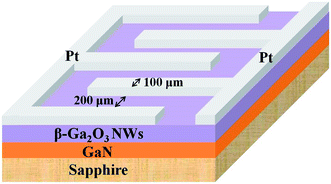 |
| | Fig. 1 Schematic diagram of fabricated β-Ga2O3 NW humidity sensor. | |
Results and discussion
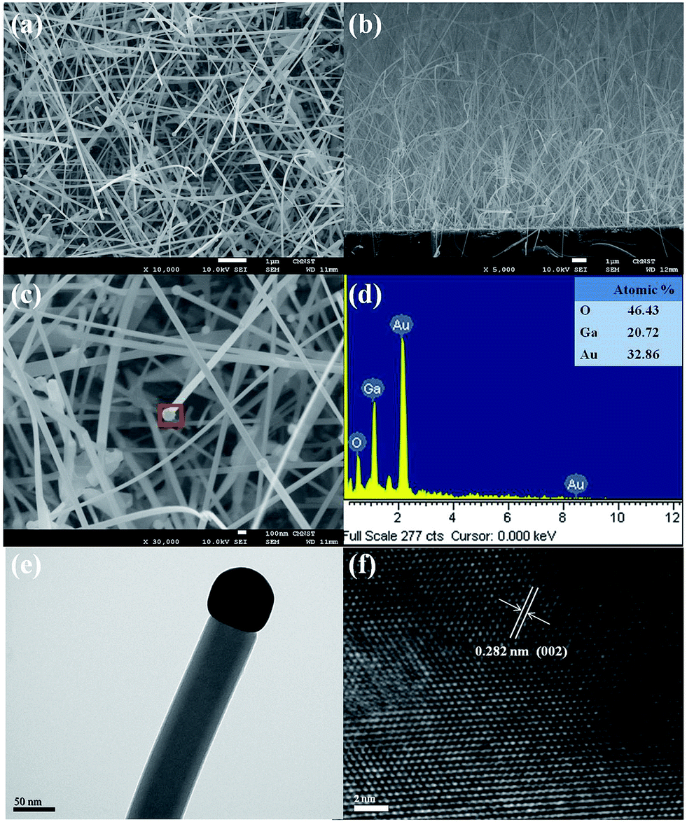
Fig. 2(a) and (b) show the top-view and cross-sectional SEM images of the as-synthesized NWs, respectively. It can be observed that randomly oriented NWs were grown on the entire GaN/sapphire template. The average diameter and length of the NWs were around 100 nm and 10 μm, respectively. As shown of Fig. 2(c) and (e), a round-shaped globule formed at the tip of the NW, which confirms that the growth of β-Ga2O3 NWs indeed occurred via the VLS process. Fig. 2(d) shows EDX spectrum taken from the red rectangle area shown in Fig. 2(c). Other than the Au-related signal, Ga- and O-related signals were also observed from the eutectic Au nanoparticle. It should be noted that only Ga- and O-related signals can be observed from the nanowires. This again indicates that the growth mechanism of Ga2O3 NWs was Au-catalyzed VLS process. Fig. 2(f) shows HRTEM image the Ga2O3 NW. The 0.282 nm lattice spacing observed from Fig. 2(f) corresponds to the d_002 spacing of β-Ga2O3. Fig. 3 shows the XRD patterns of the as-grown NWs. The sharp XRD peaks located at 2θ = 24.2°, 30.3°, 31.7°, 33.5°, 35.2°, 37.4°, 38.4°, 42.8°, 45.8°, 48.4°, 49.5°, 54.6°, 57.6°, 59.9°, 60.9°, 64.7°, 67.4°, and 77.9° can be indexed to the (201), (110), (002), (![[1 with combining macron]](https://www.rsc.org/images/entities/char_0031_0304.gif) 11), (111), (401), (
11), (111), (401), (![[3 with combining macron]](https://www.rsc.org/images/entities/char_0033_0304.gif) 11), (311), (112), (003), (402), (203), (13), (113), (020), (512), (313), and (603) planes of the β-Ga2O3 NWs, respectively. All the peaks can be assigned to monoclinic Ga2O3 with lattice constants a = 12.23 Å, b = 3.04 Å, and c = 5.8 Å (JCPDS file no. 76-0573). During the growth of the NWs, the GaN epitaxial layer decomposed into metallic Ga and N2 gas since the growth temperature was up to 1050 °C. The metallic Ga and O atoms reacted with the Au nanoparticles to form the Au–Ga2O3 alloy. This nanosized alloy acted as the catalyst to absorb gas-phase reactants, and then formed the eutectic alloy. As the concentration of the reactant in the liquidized globules became oversaturated, precipitation began and 1-D Ga2O3 NWs formed.
11), (311), (112), (003), (402), (203), (13), (113), (020), (512), (313), and (603) planes of the β-Ga2O3 NWs, respectively. All the peaks can be assigned to monoclinic Ga2O3 with lattice constants a = 12.23 Å, b = 3.04 Å, and c = 5.8 Å (JCPDS file no. 76-0573). During the growth of the NWs, the GaN epitaxial layer decomposed into metallic Ga and N2 gas since the growth temperature was up to 1050 °C. The metallic Ga and O atoms reacted with the Au nanoparticles to form the Au–Ga2O3 alloy. This nanosized alloy acted as the catalyst to absorb gas-phase reactants, and then formed the eutectic alloy. As the concentration of the reactant in the liquidized globules became oversaturated, precipitation began and 1-D Ga2O3 NWs formed.
 |
| | Fig. 2 (a) Top-view and (b) cross-sectional SEM images of as-synthesized β-Ga2O3 NWs. (c) Magnified SEM image of (a), and (d) EDX spectrum taken from red rectangle area in (c). (e) TEM image of a single β-Ga2O3 NW, and (f) high-resolution TEM image. | |
 |
| | Fig. 3 XRD patterns of as-synthesized β-Ga2O3 NWs. | |
Fig. 4(a) shows the currents measured for the β-Ga2O3 NWs with a 5 V applied bias for various RH values at 25 °C. The measured current increased monotonically when RH was increased from 30% to 95%. The measured current was stable with negligible fluctuation after 20 min of testing. For n-type β-Ga2O3 NW humidity sensors, it has been reported that water vapor adsorbs onto the surface, replacing the previously adsorbed ionized oxygen. The reactive mechanism is:15,16
| | |
H2O(ads) + O2− ↔ 2H2O2 + e−
| (1) |
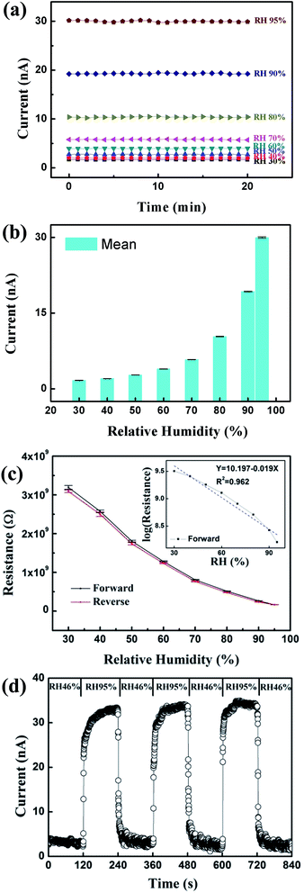 |
| | Fig. 4 (a) Current measured for β-Ga2O3 NW humidity sensor at various RH values. (b) Mean values of current with error bars at various RH values. (c) Forward and reverse resistance measured in range of RH 30–95%. Inset plots the log resistance as a function of RH. (d) Dynamic response measured for β-Ga2O3 NWs humidity sensor between RH 46% and 95%. | |
This reaction releases trapped electrons, which increases the concentration of electrons and thus decreases the resistance of the surface layer of β-Ga2O3 NWs. At low RH, the adsorbed water molecules are distributed on the NW surface. The trapped electrons are released by the adsorption of water, which contributes to the increase of conductivity at low RH. With high RH, it has been reported that the adsorbed water may gradually form a monolayer on the NW surface. The hydrogen bonds are then generated from the adsorbed monolayer water, leading to a water dissociation process:16,17
The generated H+ (or H3O+) and OH− ions contribute to the sharp increase of conductivity at high RH. Therefore, at high RH, more H+ (or H3O+) and OH− ions form, and thus conductivity increases with a further increase of RH. In Fig. 4(a), the current measured at RH 30% was 1.8 nA, and that at RH 95% was 30 nA. It can also be observed that the increase in the current at high RH was much higher (>60%) than that at low RH (<60%). Fig. 4(b) shows the mean values of Fig. 4(a) with error bars at various RH values. To investigate the vapor adsorption/desorption behavior of the β-Ga2O3 NW humidity sensor, Fig. 4(c) plots the forward and reverse currents as a function of RH. The measurement was conducted from RH 30% to 95%, and then from RH 95% to 30%. The variation between the forward and reverse measurements was small, with a hysteresis value of 5.4%. The inset in Fig. 4(c) plots the log resistance as a function of RH for the forward measurement. The measured log resistance decreased, which shows good linearity (Y = 10.197 − 0.019X and R2 = 0.962) for RH from 30% to 95%.
Fig. 4(d) shows the dynamic response measured for the β-Ga2O3 NWs with a 5 V applied bias. One chamber with 46% RH was prepared using compressed dry air, and the original controllable chamber was kept at RH 95%. During this measurement, the sample was alternately subjected to RH 46% and 95% while the temperature was controlled at 25 °C. The measured current increased as the RH was increased from 46% to 95%, and decreased to around its initial value when the RH was decreased from 95% to 46%. This result indicates that the sensing properties of β-Ga2O3 NWs were stable. When changing from RH 46% to 95% and then back to 46%, the response and recovery times, defined as the time taken to reach 90% of the saturated state, are important characteristics of humidity sensors. For the VLS-grown β-Ga2O3 NWs, the average response and recovery times were around 18 and 13 s, respectively.
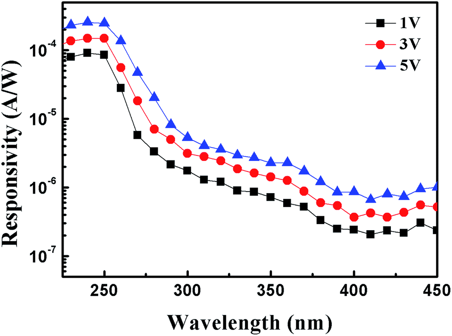
Fig. 5 shows the UV spectral responses of the fabricated β-Ga2O3 NW sample at room temperature. During the measurement, a 300 W Xe lamp dispersed by a monochromator was used as the excitation source. The monochromatic light, calibrated with a UV-enhanced Si diode and an optical power meter, was then modulated by a mechanical chopper and collimated onto the front side of the fabricated devices using an optical fiber. The photocurrent was subsequently recorded using a lock-in amplifier. It was found that the photoresponse of the fabricated β-Ga2O3 NW sample was flat in the short-wavelength region and had a sharp cutoff at 250 nm. With an incident light wavelength of 250 nm and an applied bias of 1 V, the measured responsivity of the photodetector was 8.54 × 10⁻⁵ mA W−1. When the bias voltage was increased to 5 V, the measured responsivity increased to 2.47 × 10⁻⁴ mA W−1. In other words, the responsivity increased significantly with increasing applied bias, which suggests that there was a photoconductive gain in the photodetector.18
 |
| | Fig. 5 Room-temperature spectral response of β-Ga2O3 NWs with various applied biases. | |
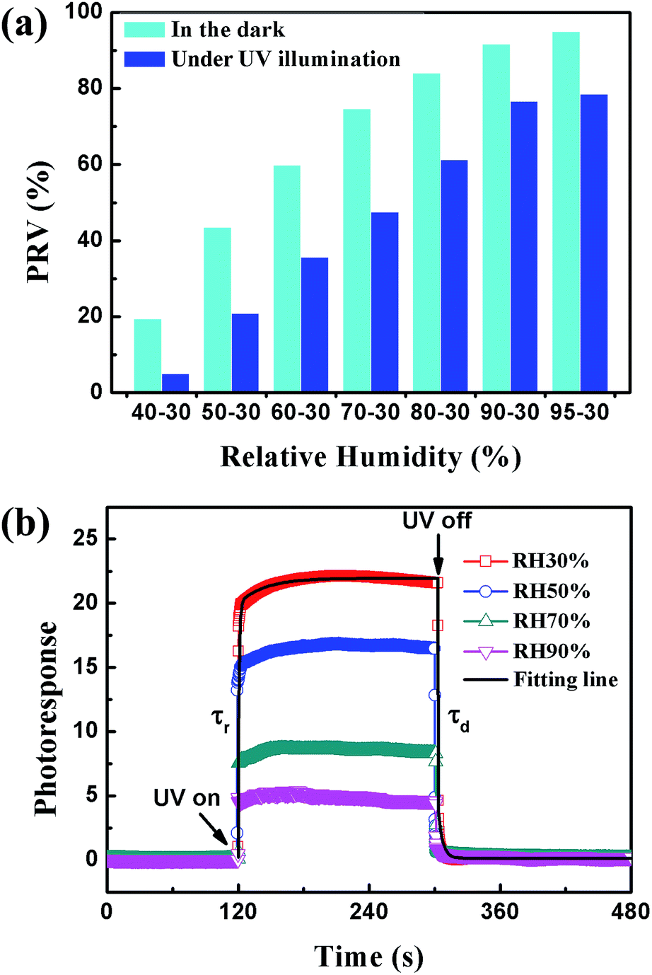
To determine the sensing relationship of β-Ga2O3 NWs between UV and humidity, the effect of UV illumination on the humidity properties and the effect of RH on the UV responses were measured, respectively. Fig. 6(a) shows the measurements of β-Ga2O3 NW humidity properties in the dark and under 254 nm UV light illumination. It plots the percentage resistance variation (PRV) between two RH values. The PRV is defined as:
| |
 | (4) |
where
R30 is the resistance at RH 30% and
R is the resistance at a certain RH level. The results show that PRV increased with increasing RH both in the dark and under UV illumination. The resistance of β-Ga
2O
3 NWs in the dark was much higher than that under UV illumination (
Table 1). For a certain low RH level in the dark (
Fig. 7(a)), a large number of O
2 molecules adsorbed onto the surface of β-Ga
2O
3 NWs [O
2(gas) ↔ O
2(ads), O
2(ads) + e
− ↔ O
2−]. The adsorbed oxygen receives free electrons from β-Ga
2O
3 NWs, forming negatively charged oxygen species, which reduces the carrier concentration and forms a depletion layer on the surface of β-Ga
2O
3 NWs. This mechanism significantly decreases β-Ga
2O
3 conductivity due to the large surface-to-volume ratio of NWs. Upon exposure to UV light under the same RH level, the adsorption of UV light generates electron–hole pairs on the surface of the NWs. The photogenerated holes migrate to the surface and oxidize the adsorbed negatively charged oxygen ions on the surface [O
2−(ads) + h
+ → O
2(gas)]. The O
2 molecules are then released and the depletion layer of β-Ga
2O
3 NWs is reduced. The remaining photogenerated electrons lead to an increase in conductivity (
Table 1).
19–21 The PRV values obtained in the dark were all higher than those obtained under UV illumination at each RH (
Fig. 6(a)). Without UV illumination at low RH (
Fig. 7(a)), some water molecules adsorbed on the NW surface, resulting in the release of trapped electrons, which led to an increase of PRV with increasing RH. When the NWs were illuminated by UV light at low RH, some of the adsorbed oxygen ions (O
2−) were oxidzed by the UV-photogenerated holes. This process reduces the number of O
2− on the NW surface, which results in fewer O
2− ions to react with water vapor. In other words, more O
2− adsorbed on the NW surface can react with water vapor in the dark, resulting in higher PRV than that obtained under UV illumination (
Fig. 6(a)). At high RH without UV illumination, the dissociated water provides ionic conductivity, which dominates the main effect on dark conductivity (
eqn (2) and
(3)). The lower PRV increase of the UV-illuminated NWs is due to two main reasons. Firstly, at high RH in the dark, the number of O
2− ions sharply decreased due to the formation of monolayer water on the NW surface. The remaining O
2− ions can still be replaced by water vapour, resulting in the release of some electrons to the NWs. However, under UV illumination, most of the remaining O
2− ions are oxidized by the photogenerated holes, which decreases the number of carriers in the NWs. Secondly, the dissociated H
+ and OH
− ions from water vapor at high RH can be captured by the UV-light-generated electrons and holes, leading to low conductance.
22–24 To further understand the interactive effect between UV and humidity,
Fig. 6(b) shows the measurements of the photocurrent as a function of time obtained with UV switched on and off at various RH values. To quantify the current change of the device under UV illumination, the photoresponse is defined as:
| | |
Photoresponse = (IUV − Idark)/Idark
| (5) |
where
IUV and
Idark are the currents with and without UV illumination, respectively. The photoresponses calculated from
Fig. 6(b) are around 22.07, 16.82, 8.62, and 4.97 for RH values of 30%, 50%, 70%, and 90%, respectively. These results indicate that β-Ga
2O
3 NWs have a higher UV response under lower RH. At low RH, the adsorbed H
2O molecules are distributed on the surface of the β-Ga
2O
3 NWs. With UV illumination, the photogenerated holes react with oxygen ions on the surface, and the remaining photogenerated electrons lead to an increase in NW conductivity. However, at high RH, the water molecules adsorbed on the surface form a water monolayer, and the generated hydrogen bonds capture electrons and holes generated by UV illumination.
22–24 This effect decreases the carrier density and photoconductivity of the NWs, resulting in a lower photoresponse. To discuss the response time of the β-Ga
2O
3 NWs at various RH values, the curve in
Fig. 6(b) was fitted using the following equation:
25–27| | |
I = I0 + Ae−t/τ1 + Be−t/τ2
| (6) |
where
I0 is the steady-state photocurrent,
t is the time,
A and
B are constants, and
τ1 and
τ2 are relaxation time constants. The constant
τ1 is related to the rapid change of the carrier concentration when the UV light is turned on/off, and
τ2 is related to carrier trapping and release due to the oxygen vacancy defects in the NWs. The fitted values of
τr and
τd of the β-Ga
2O
3 NWs are summarized in
Table 2. The β-Ga
2O
3 NWs have the fastest rise time (1.36 s) and decay time (1.8 s) at RH 90%. Li
et al. reported that the fast decay time when UV is switched off is attributed to the rapid recombination of holes with electrons. The slow decay time is due to the re-adsorption of oxygen on the surface. The fast decay process dominates the current recovery at high RH, whereas the slow decay process dominates the recovery at low RH.
24,28,29 The results of
Fig. 6(b) also confirm this mechanism, with the current at RH 30% having a longer recovery time than that at RH 90%.
 |
| | Fig. 6 (a) Humidity PRV of β-Ga2O3 NWs measured in the dark and UV illumination. (b) Time-dependent photoresponse of β-Ga2O3 NWs at various RH values with UV switched on/off. | |
Table 1 Resistances of the β-Ga2O3 NWs calculated from RH 30% to 95% in the dark and under UV illumination
| Resistance (107 Ω) |
| RH (%) |
30 |
40 |
50 |
60 |
70 |
80 |
90 |
95 |
| Dark |
319.4 |
257.5 |
180.6 |
128.2 |
80.9 |
51.3 |
26.7 |
16.1 |
| UV |
7.3 |
6.9 |
5.8 |
4.7 |
3.8 |
2.8 |
1.7 |
1.6 |
 |
| | Fig. 7 Schematics of oxygen and water molecules on surface of β-Ga2O3 NWs at (a) low and (b) high RH in the dark and under UV illumination. | |
Table 2 Rise and decay times fitted from photoresponse for various RH values
| RH% |
30 |
50 |
70 |
90 |
| Rise time (s) |
24.94 |
23.76 |
7.25 |
1.36 |
| Decay time (s) |
6.24 |
3.97 |
2.5 |
1.8 |
Conclusions
The growth of β-Ga2O3 NWs on a GaN/sapphire template and the fabrication of a β-Ga2O3 NW photodetector and humidity sensor were reported. The measured current of the β-Ga2O3 NW humidity sensor increased monotonically when RH was increased from 30% to 95% in the dark. Both under UV illumination and in the dark, PRV increased with increasing RH. At low RH, some of the adsorbed O2− are oxidized by the UV-photogenerated holes, resulting in fewer O2− ions to react with water vapor. At high RH, the dissociated ions from water vapor can be captured by the UV-light-generated electrons and holes. These mechanisms contribute to the decrease of PRV under UV illumination compared to that in the dark. The photoresponse of the β-Ga2O3 NWs decreased from 22.07 to 4.97 when the RH was increased from 30% to 95%. The dissociated ions from water vapor at high RH influence the carrier density of the NWs, resulting in a lower photoresponse. However, the β-Ga2O3 NWs show fast rise and decay times due to the rapid recombination of holes with electrons at high RH.
Acknowledgements
This work was supported by the Ministry of Science and Technology of Taiwan, under Contract no. MOST 103-2221-E-492-014-MY3.
Notes and references
- S. H. Song, H. H. Yang, C. H. Han, S. D. Ko, S. H. Lee and J. B. Yoon, Appl. Phys. Lett., 2012, 100, 101603 CrossRef PubMed.
- E. L. Tan, W. N. Ng, R. Shao, B. D. Pereles and K. G. Ong, Sensors, 2007, 7, 1747–1756 CrossRef PubMed.
- L. T. Chen, C. Y. Lee and W. H. Cheng, Sens. Actuators, A, 2008, 147, 522–528 CrossRef CAS PubMed.
- A. K. Kalkan, H. D. Li, C. J. O'Brien and S. J. Fonash, IEEE Electron Device Lett., 2004, 25, 526–528 CrossRef CAS.
- H. T. Hsueh, T. J. Hsueh, S. J. Chang, F. Y. Hung, C. L. Hsu, B. T. Dai, K. T. Lam and K. H. Wen, IEEE Trans. Nanotechnol., 2012, 11, 520–525 CrossRef.
- F. Liang, L. B. Luo, C. K. Tsang, L. Zheng, H. Cheng and Y. Y. Li, Mater. Res. Bull., 2012, 47, 54–58 CrossRef CAS PubMed.
- N. K. Pandey, K. Tiwari and A. Roy, IEEE Sens. J., 2011, 11, 2911–2918 CrossRef CAS.
- Q. Kuang, C. Lao, Z. L. Wang, Z. Xie and L. Zheng, J. Am. Chem. Soc., 2007, 129, 6070–6071 CrossRef CAS PubMed.
- C. Yuan, Y. Xu, Y. Deng, N. Jiang, N. He and L. Dai, Nanotechnology, 2010, 21, 415501 CrossRef PubMed.
- J. S. Kim, H. E. Kim, H. L. Park and G. C. Kim, Solid State Commun., 2004, 132, 459–463 CrossRef CAS PubMed.
- N. Ueda, H. Hosono, R. Waseda and H. Kawazoe, Appl. Phys. Lett., 1997, 70, 3561–3563 CrossRef CAS PubMed.
- S. P. Arnold, S. M. Prokes, F. K. Perkins and M. E. Zaghloul, Appl. Phys. Lett., 2009, 95, 103102 CrossRef PubMed.
- W. Y. Weng, T. J. Hsueh, S. J. Chang, G. J. Huang and S. P. Chang, IEEE Photonics Technol. Lett., 2010, 22, 709–711 CrossRef CAS.
- K. Liu, M. Sakurai and M. Aono, Small, 2012, 8, 3599–3604 CrossRef CAS PubMed.
- C. Lai, X. Wang, Y. Zhao, H. Fong and Z. Zhu, RSC Adv., 2013, 3, 6640–6645 RSC.
- J. M. K. Nobbs, J. Phys. Chem. Solids, 1968, 29, 439–450 CrossRef CAS.
- G. Y. Chai, L. Chow, O. Lupan, E. Rusu, G. I. Stratan, H. Heinrich, V. V. Ursaki and I. M. Tiginyanu, Solid State Sci., 2011, 13, 1205–1210 CrossRef CAS PubMed.
- J. A. Garrido, E. Monroy, I. Izpura and E. Munoz, Semicond. Sci. Technol., 1998, 13, 563–568 CrossRef CAS.
- C. L. Hsu, H. H. Li and T. J. Hsueh, ACS Appl. Mater. Interfaces, 2013, 5, 11142–11151 CAS.
- J. M. Bao, I. Shalish, Z. H. Su, R. Gurwitz, F. Capasso, X. W. Wang and Z. F. Ren, Nanoscale Res. Lett., 2011, 6, 404 CrossRef PubMed.
- O. Lupan, G. Chai, L. Chow, G. A. Emelchenko, H. Heinrich, V. V. Ursaki, A. N. Gruzintsev, I. M. Tiginyanu and A. N. Redkin, Phys. Status Solidi A, 2010, 207, 1735–1740 CrossRef CAS PubMed.
- Y. Takahashi, M. Kanamori, A. Kondoh, H. Minoura and Y. Ohya, Jpn. J. Appl. Phys., Part 1, 1994, 33, 6611–6615 CrossRef CAS.
- Q. H. Li, T. Gao, Y. G. Wang and T. H. Wang, Appl. Phys. Lett., 2005, 86, 123117 CrossRef PubMed.
- Y. Li, F. Della Valle, M. Simonnet, I. Yamada and J.-J. Delaunay, Appl. Phys. Lett., 2009, 94, 023110 CrossRef PubMed.
- J. Reemts and A. Kittel, J. Appl. Phys., 2007, 101, 013709 CrossRef PubMed.
- N. Liu, G. Fang, W. Zeng, H. Zhou, F. Cheng, Q. Zheng, L. Yuan, X. Zou and X. Zhao, ACS Appl. Mater. Interfaces, 2010, 2, 1973–1979 CAS.
- D. Guo, Z. Wu, P. Li, Y. An, H. Liu, X. Guo, H. Yan, G. Wang, C. Sun, L. Li and W. Tang, Opt. Mater. Express, 2014, 4, 1067–1076 CrossRef.
- S. E. Ahn, J. S. Lee, H. Kim, S. Kim, B. H. Kang, K. H. Kim and G. T. Kim, Appl. Phys. Lett., 2004, 84, 5022–5024 CrossRef CAS PubMed.
- J. B. K. Law and J. T. L. Thong, Appl. Phys. Lett., 2006, 88, 133114 CrossRef PubMed.
|
| This journal is © The Royal Society of Chemistry 2015 |
Click here to see how this site uses Cookies. View our privacy policy here.