An AuNPs-functionalized AlGaN/GaN high electron mobility transistor sensor for ultrasensitive detection of TNT

Yahui Guo ace, Xiongtao Wangad, Bin Miaoab, Ying Lid, Weirong Yaoe, Yunfei Xiee, Jiadong Li*ab, Dongmin Wu*ab and Renjun Peic
ai-Lab, Suzhou Institute of Nano-Tech and Nano-Bionics, Chinese Academy of Sciences, Suzhou 215125, China. E-mail: jdli2009@sinano.ac.cn; dmwu2008@sinano.ac.cn
bKey Laboratory of Nanodevices and Applications, Suzhou Institute of Nano-Tech and Nano-Bionics, Chinese Academy of Sciences, Suzhou 215123, China
cDivision of Nanobiomedicine, Key Laboratory for Nano-Bio Interface, Suzhou Institute of Nano-Tech and Nano-Bionics, Chinese Academy of Sciences, Suzhou 215123, China
dKey Laboratory for New Type of Functional Materials in Hebei Province, School of Material and Engineering, Hebei University of Technology, Tianjin 300130, China
eState Key Laboratory of Food Science and Technology, School of Food Science and Technology, Jiangnan University, Wuxi 214122, China

Received 19th August 2015 , Accepted 5th November 2015

First published on 10th November 2015


Abstract

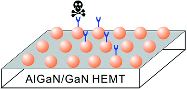
Herein, an ultrasensitive sensor based on a AlGaN/GaN high electron mobility transistor (HEMT) was developed for the detection of 2,4,6-trinitrotoluene (TNT). The sensing surface of the AlGaN/GaN HEMT grid was covalently bonded with a layer of gold nanoparticles which were functionalized with cysteamine for specific electrostatic interaction with TNT. The binding of TNT to cysteamine through donor–acceptor interactions could affect the surface charge on the gate area of the AlGaN/GaN HEMT, resulting in a gate voltage change and density changes of the 2-dimensional electron gas (2EDG) at the interface of AlGaN/GaN. By the merit of the high electron mobility of the AlGaN/GaN transistor and robust binding between cysteamine and TNT, the sensor demonstrated a fast response and excellent performance with quantitative ranges at ppt levels (from 0.1 ppt to 10 ppb) with good selectivity towards TNT. This HEMT sensor showed attractive properties for TNT detection in terms of speed, sensitivity and miniaturization.

Introduction

The development and application of gallium nitride (GaN) materials are currently at the frontier of semiconductor material research because of their outstanding electronic properties.1–3 By proper doping, the heterojunction interface between AlGaN/GaN will have a high sheet-carrier density of the two-dimensional electron-gas (2DEG) due to piezoelectricity and spontaneous polarization. The 2DEG conducting channel is very close to the surface and extremely sensitive to the adsorption of analytes.4 Heterostructure field effect transistors based on AlGaN/GaN have large breakdown voltage and high drain current density, attracting a wide range of applications in analytical chemistry and biochemistry.5 Ultrasensitive AlGaN/GaN high electron mobility transistor (HEMT) sensor has been successfully employed to detect the prostate specific antigen,6,7 glucose8 and other substances.9–11

Trace explosive detection in counter-terrorism calls for ultrasensitive and minimized apparatus.12 Moreover, explosives used in mining could also contaminate the soil and water in environment, exhibiting toxicity to humans, animals and plants. TNT (2,4,6-trinitrotoluene) is one of the most commonly used explosives, and it was reported that the maximum concentration of TNT that human body can withstand is 2.0 ppb.13 Conventional methods based on mass spectrometry,14 ion mobility spectrometry,15 fluorescence,16 electrochemistry,17 Raman spectroscopy18 have been developed for trace detection of TNT. But all these methods require bulky instruments or tedious preparation processes. For practical reasons, there is a strong demand to develop miniaturized sensors for fast, real-time and sensitive detection of ultra-trace TNT. Miniaturized sensors based on one-dimensional nanomaterials, such as silicon nanowires,19 metal oxide nanowires20 and carbon nanotubes,21 have been realized for TNT detection in many research labs. However, it is rather difficult for those sensors to achieve reproducibility due to the random growth of the sensitive nanostructures. To address this issue, Wang et al. designed a silicon nanowire-based sensor fabricated by lithography method.22 However, the Si-FET is chemically unstable and degradation of silicon oxide gate insulator in aqueous solutions has not been successfully addressed yet.23,24

There is no report on the detection of explosives by AlGaN/GaN HEMT sensor. In this work, we developed a gold nanoparticle (AuNPs) functionalized AlGaN/GaN HEMT sensor for fast and ultrasensitive detection of TNT. AuNPs was proved to help reduce false positives and negatives when device-to-device variability exists.25 In a previous work, AuNPs were physically absorbed on the transistor surfaces for kinase detection.26 The solution of AuNPs were spotted onto the wafer directly and dried in a vacuum desiccator. It was easy to cause aggregation and exfoliation from the surface. Differently, in our strategy 3-mercaptopropyltriethoxysilane (MPTES) was used to functionalize the surface of gate electrode for anchoring AuNPs by strong Au–S bond. Thus, AuNPs can be firmly immobilized on the surface, with large surface area for modification of probe ligands (cysteamine in the present work). The fabricated sensor in the present work exhibited a detection response of TNT from 0.1 ppt to 10 ppb, and responded rapidly with good selectivity. The fabricated transistor sensors showed great potential in analytical sciences in virtue of ultrahigh sensitivity, fast response and easy to miniaturization by using integrated circuit technology.

Experimental

Chemicals and materials

2,4,6-Trinitrotoluene (TNT) and its analogues were purchased from Aladdin Industrial Inc. (Shanghai, China). Stock solutions of TNT were prepared in ultrapure water. Cysteamine was purchased from Sigma-Aldrich Co. LLC. (Shanghai, China). 3-Mercaptopropyltriethoxysilane (MPTES) was purchased from Energy Chemical (Shanghai, China). All other chemical reagents were of analytical reagent grade and used without further purification. Measurements were performed in 0.1 mM PBS (pH 7.4 at 25 °C).

Citrate-stabilized GNPs were prepared by thermal reduction of HAuCl4 with sodium citrate.27 Briefly, a sodium citrate solution (1%, 2.0 mL) was rapidly added to a boiled HAuCl4 solution under vigorous stirring, and the mixed solution was boiled for 20 min. Then, the resulting solution was cooled to room temperature and stored at 4 °C before use. The UV-vis spectrum of synthesized AuNPs was recorded as shown in Fig. S1 in the ESI.

Sensor fabrication and modification

The sapphire substrate, capped with 1.5 μm non-doped GaN, 18 nm AlGaN and 1.5 nm GaN respectively, was supplied by School of Microelectronics, Xidian University. As depicted in Fig. 1, the AlGaN/GaN HEMT was fabricated as follow:
image file: c5ra16704c-f1.tif
Fig. 1 Illustration of the fabrication process of AlGaN/GaN HEMT: (I) mesa etching; (II) ohmic contact; (III) sputtering electrode; (IV) silicone encapsulation.

(I) After cleaning, the GaN cap layer was spin-coated with photoresist AZ5214 (2 μm). Then the photoresist was baked at 95 °C for 1.5 min, which was followed by photolithography using an EV620 aligner to define the mesa pattern. Mesa isolation was performed by inductively coupled plasma etching with Cl2/BCl3 (mesa height is 50 nm).

(II) The resulted substrate was then spin-coated with photoresist AZ4620 and the ohm contact window was opened after photolithography and development. Ti/Al/Ni/Au multilayer for the ohm contact was then deposited by using e-beam evaporation system. After that, the samples were introduced into a rapid thermal processing system (RTP-500, at 880 °C for 45 s) for annealing under a flow of nitrogen ambient. The ohmic contact electrode size is 2 mm × 2 mm, and source electrode distance and drain electrode spacing is 2 mm;

(III) The overlay layer mask was transferred into the ohmic contact layer by photolithography (with a Shipley AZ5214 photoresist). Ni/Au multilayer was then deposited by an e-beam evaporation system to form the source and drain electrodes.

(IV) Silicone was employed for device packaging to protect the source/drain electrodes.

Fig. 2 exhibited the digital photograph of manufactured AlGaN/GaN HEMT sensor chip with PDMS-packaged reaction cell (about 40 μL), and the amplified top view of fabricated transistor. The electrodes (connecting source and drain electrodes respectively) on sensor chip were connected to KEITHLEY 2636A for signal collecting. 2DEG is located at the interface between the non-doped GaN layer and the AlGaN layer. The electron mobility of the 2DEG in this device is measured to be 1672 cm2 V−1 s−1 (provided by Xidian University).


image file: c5ra16704c-f2.tif
Fig. 2 (A) Digital photograph of the AlGaN/GaN HEMT sensor chip and (B) amplified top view of the fabricated transistor. (C) Depiction of the ultrasensitive detecting device based on AlGaN/GaN HEMT sensor, the sensor chip was fixed in a black box with a mobilizable cover.

The AlGaN/GaN HEMT need to be modified on surface for TNT detection. Firstly, the surface was cleaned and oxidized by UV/O3 cleaning machine firstly. Then the device was soaked in ethanol solution containing 5% MPTES for 24 hours. After that the device was cleaned adequately by ethanol and deionized water (18 MΩ) and dried by N2. Later it was baked in the oven for 30 min at 110 °C. The AuNPs solution was diluted with water and adjusted the pH to 7.5 by NaOH. Then the modified sulfhydryl groups of MPTES on the surface were allowed to react with AuNPs in shaking table for 24 hours. After that the device was washed by deionized water and dried by N2. Then the device was immersed in the aqueous solution of 1 mM cysteamine for 24 hours. At last the device was cleaned adequately by deionized water waiting for detection.

Measurement

Fig. 2C depicted the assembled device for ultrasensitive detection based on AlGaN/GaN HEMT sensor. KEITHLEY 2636A was used to provide the required source–drain voltage (Vds) and connect to the computer which was used to collect signals during the testing process. Firstly, PBS buffer was added in the sensing region, then different concentrations of TNT were added every one hundred second and the corresponding signal was obtain as the average intensity in the 30–60 s plateau stage after TNT was added. Different signal response between TNT analogues and TNT was measured in the same way to investigate the selectivity of the sensor.

Results and discussion

Principle of the sensor

As illustrated in Fig. 3A, due to the spontaneous and piezoelectric polarization, there is 2DEG at the interface of non-doped GaN and modulation-doped heterojunction AlGaN, the 2DEG concentration at the AlGaN/GaN interface (ns) is given by:28
 
image file: c5ra16704c-t1.tif(1)
where εN is the permittivity of AlGaN, Vg is the applied gate voltage, Voff is the threshold voltage (inherent parameter), q is the electron charge, d is the total distance between the gate electrode and 2DEG, and Vx is the channel potential towards x direction.

image file: c5ra16704c-f3.tif
Fig. 3 (A) Illustration of the AlGaN/GaN HEMT structure for understanding the fundamental of the sensor; (B) schematic representation of the AlGaN/GaN HEMT sensor for ultrasensitive detection of TNT.

The point current between source electrode and drain electrode Ix:

 
image file: c5ra16704c-t2.tif(2)
νd is carrier mobility, μ is 2DEG electron mobility, Ex is electric-field intensity towards x direction, W is channel width, L is channel length. Source–drain current (Ids) can be calculated by integrating (2):
 
image file: c5ra16704c-t3.tif(3)

This suggests that source–drain current is associated with gate voltage. As verified in Fig. S2 in ESI, under a constant value of source–drain voltage, we got a linear relationship between gate voltage and source–drain current. The gate voltage changes 1 mV and the source–drain current will change 1.95 μA correspondingly.

The designed TNT sensor is based on the aforementioned principle. There is not an external-applied gate voltage, alternatively the slight surface charge change that caused by electrostatic interaction can induce electric potential, thus acts as the gate voltage and can result in discriminated source–drain current due to the ultrahigh electron mobility (μ) of 2DEG.

Surface charge affected by slight changes on the surface of HEMT sensor can change the gate voltage (Vg), resulting in the drain–source current change at the AlGaN/GaN interface. Fig. 3B depicts our design of the AlGaN/GaN HEMT sensor. The surface of AlGaN/GaN HEMT grid was firstly coated with MPTES, and then a layer of AuNPs were covalently modified on the surface through Au–S bond. AuNPs were functionalized with cysteamine for specific electrostatic interaction with TNT. When the electron deficient nitro of TNT approaches electron rich amino of cysteamine, the charge transfer from amino groups to aromatic rings leads to the formation of Meisenheimer complexes between TNT and primary amine groups.29 The negative charge on cysteamine is resonantly stabilized by three electron-withdrawing nitro groups and distributed throughout the molecule. The formation of the complexes could affect the gate voltage of the sensor, changing the density of 2DEG and resulting in source–drain voltaic signal changes.

Surface modification

Silane coupling agent is usually used as a bridge of organic molecules and inorganic molecules. The grid was firstly functionalized with MPTES to form a sulfhydryl-terminated monolayer on its surface. The water contact angle was tested before and after MPTES modification respectively, as shown in Fig. 4 the contact angle changed obviously after modification of MPTES, demonstrating the successful coating of MPTES.30
image file: c5ra16704c-f4.tif
Fig. 4 Connect angle test on the surface of the sensor: (A) before and (B) after the functionalization of MPTES.

AuNPs were anchored on the surface of the AlGaN/GaN HEMT sensor for easy modification and to increase the reaction area between modified probes and targets. After AuNPs were fixed on the sensor surface through strong Au–S bond, scanning electron microscope (SEM) images of the sensor surface were taken for verification. As shown in Fig. 5, the AuNPs are very well-distributed with high density. Contrast tests were conducted to demonstrate the effect of chemical-bonding for AuNPs on the AlGaN/GaN HEMT surface. AuNPs were incubated with AlGaN/GaN HEMT, which was not functionalized with MPTES, following the same modification procedures aforementioned in the Experimental section. As shown in Fig. S3 in the ESI, SEM image of the sensor showed that there were barely particles on the sensor surface. This might be due to runoff of unbounded AuNPs in washing step. Our strategy by employing chemical bonded AuNPs provides an excellent platform for further functionalization of different probing ligands.


image file: c5ra16704c-f5.tif
Fig. 5 SEM image of anchored AuNPs on the surface of AlGaN/GaN HEMT sensor.

Detection of TNT

As shown in Fig. S4, a steady signal can be obtained in 30 s after the addition of sample solutions, and the steady plateau maintained ∼30 after injection and before the next-time injection. So real-time testing can be conducted by using this sensor, especially for fast-field analysis by the merit of miniaturization. Real-time testing results by the fabricated sensor at constant bias voltage of 50 mV were shown in Fig. 6. When sample solution containing different concentration of TNT was added to the sensor cell, an abrupt peak appeared and then quickly recovered back. It was due to the mechanical disturbance when the buffer solution was added with a micropipette, since the mechanical disturbance could cause piezoelectric polarization phenomenon. Since mechanical disturbance including injection and cover moving both had influence on the signal, we just collected the steady data after injection & cover closing, and before next-time cover unfolding with an interval of 30 s, the signal intensity was collected as average value of the steady data from 30 s–60 s after injection of TNT solution (Fig. S4B). As shown in Fig. 6A, the signal intensity changes was dependent on TNT in the concentration range from 0.1 ppt to 10 ppb. A clear responding relationship [y = 0.524 × ln(0.825 × ln(x)) (R2 = 0.984)] was got between signal changes with various concentrations of TNT (Fig. 6B).
image file: c5ra16704c-f6.tif
Fig. 6 (A) Real-time detection of increasing concentrations of TNT. (B) The signal intensity change with different concentration of TNT in PBS buffer. The data were obtained as the average intensity in the time of 30–60 s after TNT was added to the detecting system.

As shown in Fig. 7, the sensor also showed good selectivity towards TNT. Analogues including 2,6-dinitrotoluene (2,6-DNT), 2-nitrotoluene (ONT), 3-nitrotoluene (MNT), 4-nitrotoluene (PNT) and toluene (PhMe) at the concentration of 10 ppb did not cause obvious signal changes. The nitro-substituted aromatic molecules with stronger electron-withdrawing nature, such as TNT and 2,6-DNT, induce a larger conductivity change than those nitro-substituted aromatic molecules with less electron-withdrawing nature (such as ONT), suggesting the former molecules have a higher ability to create charge-transfer complexes with the functional amino groups. In stark contrast, at concentrations higher than 10 ppb, all these analogical molecules have no observable signal changes compared with 100 ppt TNT, which demonstrated that it is suitable for the ultra-trace detection of TNT with satisfying selectivity.


image file: c5ra16704c-f7.tif
Fig. 7 Selectivity test towards TNT. All the concentrations of the compounds were 10 ppb, except TNT (100 ppt).

Conclusions

In conclusion, we have successfully developed an AlGaN/GaN HEMT sensor for ultrasensitive and fast detection of TNT. It can be used to detect TNT in an ultralow concentration ranges (from 0.1 ppt to 10 ppb). Moreover, the sensor had a high selectivity toward TNT over its analogous compounds. These results indicated that the fabricated AuNPs-modified AlGaN/GaN HEMT sensor provides a promising platform for TNT detection with great practical potential in term of speed, sensitivity and miniaturization.

Acknowledgements

This work has been supported by NSFC Project (No. 61104226, 21275156, 61573346), Youth Innovation Promotion Association CAS (2014278), Jiangsu Province Science and Technology Support Program (BE2013056), and the Fundamental Research Funds for the Central Universities (JUSRP115A25). We thank the Nano-Characterization and Nano-Fabrication Platforms at the Suzhou Institute of Nano-Tech and Nano-Bionics, Chinese Academy of Sciences for the fabrication and characterization support.

Notes and references

  1. S. F. Chichibu, A. Uedono, T. Onuma, B. A. Haskell, A. Chakraborty, T. Koyama, P. T. Fini, S. Keller, S. P. Denbaars, J. S. Speck, U. K. Mishra, S. Nakamura, S. Yamaguchi, S. Kamiyama, H. Amano, I. Akasaki, J. Han and T. Sota, Nat. Mater., 2006, 5, 810–816 CrossRef CAS PubMed.
  2. R. Kirste, N. Rohrbaugh, I. Bryan, Z. Bryan, R. Collazo and A. Ivanisevic, Annu. Rev. Anal. Chem., 2015, 8, 149–169 CrossRef CAS PubMed.
  3. H. M. Zhang, Y. Sun, W. Li, J. P. Peng, C. L. Song, Y. Xing, Q. Zhang, J. Guan, Z. Li, Y. Zhao, S. Ji, L. Wang, K. He, X. Chen, L. Gu, L. Ling, M. Tian, L. Li, X. C. Xie, J. Liu, H. Yang, Q. K. Xue, J. Wang and X. Ma, Phys. Rev. Lett., 2015, 114, 107003 CrossRef PubMed.
  4. J. Cheng, J. Li, B. Miao, J. Wang, Z. Wu, D. Wu and R. Pei, Appl. Phys. Lett., 2014, 105, 083121 CrossRef.
  5. Y. J. Lee, Y. C. Yao, C. Y. Huang, T. Y. Lin, L. L. Cheng, C. Y. Liu, M. T. Wang and J. M. Hwang, Nanoscale Res. Lett., 2014, 9, 433 CrossRef PubMed.
  6. B. S. Kang, H. T. Wang, T. P. Lele, Y. Tseng, F. Ren, S. J. Pearton, J. W. Johnson, P. Rajagopal, J. C. Roberts, E. L. Piner and K. J. Linthicum, Appl. Phys. Lett., 2007, 91, 112106 CrossRef.
  7. J. D. Li, J. J. Cheng, B. Miao, X. W. Wei, J. Xie, J. C. Zhang, Z. Q. Zhang and D. M. Wu, J. Micromech. Microeng., 2014, 24, 075023 CrossRef.
  8. B. H. Chu, B. S. Kang, S. C. Hung, K. H. Chen, F. Ren, A. Sciullo, B. P. Gila and S. J. Pearton, J. Diabetes Sci. Technol., 2010, 4, 171–179 CrossRef PubMed.
  9. T. Lalinský, I. Rýger, G. Vanko, M. Tomáška, I. Kostič, S. Haščík and M. Vallo, Procedia Eng., 2010, 5, 152–155 CrossRef.
  10. G. M. Muntze, B. Baur, W. Schafer, A. Sasse, J. Howgate, K. Roth and M. Eickhoff, Biosens. Bioelectron., 2015, 64, 605–610 CrossRef PubMed.
  11. Y. Alifragis, A. Volosirakis, N. A. Chaniotakis, G. Konstantinidis, A. Adikimenakis and A. Georgakilas, Biosens. Bioelectron., 2007, 22, 2796–2801 CrossRef CAS PubMed.
  12. X. Liu, L. Zhao, H. Shen, H. Xu and L. Lu, Talanta, 2011, 83, 1023–1029 CrossRef CAS PubMed.
  13. N. Tu and L. Wang, Chem. Commun., 2013, 49, 6319–6321 RSC.
  14. F. Bianchi, A. Gregori, G. Braun, C. Crescenzi and M. Careri, Anal. Bioanal. Chem., 2015, 407, 931–938 CrossRef CAS PubMed.
  15. S. Cheng, J. Dou, W. Wang, C. Chen, L. Hua, Q. Zhou, K. Hou, J. Li and H. Li, Anal. Chem., 2013, 85, 319–326 CrossRef CAS PubMed.
  16. Y. Ma, S. Huang and L. Wang, Talanta, 2013, 116, 535–540 CrossRef CAS PubMed.
  17. H. Ma, L. Yao, P. Li, O. Ablikim, Y. Cheng and M. Zhang, Chemistry, 2014, 20, 11655–11658 CrossRef CAS PubMed.
  18. S. S. Dasary, A. K. Singh, D. Senapati, H. Yu and P. C. Ray, J. Am. Chem. Soc., 2009, 131, 13806–13812 CrossRef CAS PubMed.
  19. Y. Engel, R. Elnathan, A. Pevzner, G. Davidi, E. Flaxer and F. Patolsky, Angew. Chem., Int. Ed., 2010, 49, 6830–6835 CrossRef CAS PubMed.
  20. D. Wang, A. Chen and A. K. Jen, Phys. Chem. Chem. Phys., 2013, 15, 5017–5021 RSC.
  21. T. H. Kim, B. Y. Lee, J. Jaworski, K. Yokoyama, W. J. Chung, E. Wang, S. Hong, A. Majumdar and S. W. Lee, ACS Nano, 2011, 5, 2824–2830 CrossRef CAS PubMed.
  22. D. Wang, H. Sun, A. Chen, S. H. Jang, A. K. Jen and A. Szep, Nanoscale, 2012, 4, 2628–2632 RSC.
  23. J. Yu, S. K. Jha, L. Xiao, Q. Liu, P. Wang, C. Surya and M. Yang, Biosens. Bioelectron., 2007, 23, 513–519 CrossRef CAS PubMed.
  24. A. Podolska, L. C. Hool, K. D. G. Pfleger, U. K. Mishra, G. Parish and B. D. Nener, Sens. Actuators, B, 2013, 177, 577–582 CrossRef CAS.
  25. M. S. Makowski, S. Kim, M. Gaillard, D. Janes, M. J. Manfra, I. Bryan, Z. Sitar, C. Arellano, J. Xie, R. Collazo and A. Ivanisevic, Appl. Phys. Lett., 2013, 102, 74102 CrossRef PubMed.
  26. M. S. Makowski, I. Bryan, Z. Sitar, C. Arellano, J. Xie, R. Collazo and A. Ivanisevic, Appl. Phys. Lett., 2013, 103, 13701 CrossRef PubMed.
  27. C. A. Mirkin, R. L. Letsinger, R. C. Mucic and J. J. Storhoff, Nature, 1996, 382, 607–609 CrossRef CAS PubMed.
  28. D. A. Neamen, in Semiconductor Physics and Devices, ed. K. Butcher, McGraw-Hill Companies, Inc., 2007, pp. 110–113 Search PubMed.
  29. A. K. Jamil, E. L. Izake, A. Sivanesan and P. M. Fredericks, Talanta, 2015, 134, 732–738 CrossRef CAS PubMed.
  30. Y. Tan and T. Wei, Talanta, 2015, 141, 279–287 CrossRef CAS PubMed.

Footnotes

Electronic supplementary information (ESI) available. See DOI: 10.1039/c5ra16704c
X. Wang and Y. Guo contributed equally to this work.

This journal is © The Royal Society of Chemistry 2015
Click here to see how this site uses Cookies. View our privacy policy here.