
Large-area MoS2 thin layers directly synthesized on Pyramid-Si substrate for surface-enhanced Raman scattering
Hengwei Qiua,
Zhen Lia,
Saisai Gaoa,
Peixi Chena,
Chao Zhanga,
Shouzhen Jiang*a,
Shicai Xub,
Cheng Yanga and
Hongsheng Lic
aSchool of Physics and Electronics, Shandong Normal University, Jinan 250014, People's Republic of China. E-mail: jiang_sz@126.com
bCollege of Physics and Electronic Information, Shandong Provincial Key Laboratory of Functional Macromolecular Biophysics, Institute of Biophysics, Dezhou University, Dezhou 253023, People's Republic of China
cDepartment of Radiation Oncology, Key Laboratory of Radiation Oncology of Shandong Province, Shandong Cancer Hospital and Institute, Jinan 250117, People's Republic of China
First published on 29th September 2015
Abstract
In our work, we directly synthesized few layer MoS2 on a pyramid-Si substrate to fabricate a surface-enhanced Raman scattering (SERS) substrate via thermally decomposing the precursor of ammonium thiomolybdate ((NH4)2MoS4). Scanning electron microscopy (SEM), atomic force microscopy (AFM), X-ray diffraction (XRD) and Raman spectra are employed to characterize the as-grown MoS2 layers. Adenosine and cytidine were selected as the probe molecules to investigate the SERS ability of the MoS2-pyramid-Si substrate, and have shown that the MoS2-pyramid-Si substrate can prominently suppress photobleaching and fluorescence of the probe molecule. Compared with the MoS2-flat-Si substrate (MoS2 layers synthesized on flat-Si substrate), the MoS2-pyramid-Si substrate has more significant SERS ability. The minimum detected concentration of both adenosine and cytidine on the MoS2-pyramid-Si substrate can reach 10−6 M. Importantly, the linear relationship between the Raman intensity and the concentration of adenosine or cytidine can apply to the bimolecular detection. This work may provide a new opportunity for the study of the chemistry mechanism (CM) and novel SERS substrate fabrication.
1. Introduction
In recent years, SERS as a powerful tool for biomedical detection with nondestructive, ultrasensitive and real-time features has attracted increasing attention.1–3 The commonly used SERS substrates are metal nanostructures include Ag, Au, Cu and Ni in the forms of nanoparticles or rough surfaces and semiconductor substrates include ZnO, ZnS, TiO2, CuO, CdTe and SnO2. However, the instability and poor biocompatibility of the metal nanoparticles have become the obstacle of the SERS substrate development.4,5 Furthermore, the lower adsorption capacity of metal nanostructures for some molecules often limits their applications.6 With the rapid development of the SERS technology due to its superior performance in applications, a variety of novel SERS substrates emerge in endlessly, include graphene and MoS2.MoS2, which is a ultrathin 2D layered material analogous to graphene, has created great interest due to its great potential in the fields of catalysis, microelectronics, lithium batteries, hydrogen storage, dry lubricant, medical and optoelectronics.7–13 In form, the layered MoS2, where the Mo layer is sandwiched between two sulfur layers by covalent forces.14 Compare with graphene, easier bio-modification of MoS2 can be more widely used in biosensor. Recent research indicated that MoS2 films have Raman enhancement effect, which may cause by charge transfer and dipole–dipole coupling.15 Nowadays, the SERS substrates based on graphene or graphene–metal nanostructure have been already matured,16–19 but the SERS substrate fabrication based on MoS2 is still at primary stage. Importantly, MoS2 with the high light transmission, chemical stability, biomolecular affinity and low-temperature synthesis, undoubtedly can be an ideal platform to support SERS active. Porous Si possesses large specific area and governable nanoporous structure, which can increase the amount of the effective hot spots and further enhance the sensitivity of the SERS signals.20–22 Recently, some groups have reported different SERS substrates based the porous Si, such as porous Si decorated with Au nanoparticles23,24 and Ag-coated Si nanoporous.25,26
Here, we present a MoS2-pyramid-Si SERS substrate with demonstrated low concentration sensitivity. Compare with graphene, large-size MoS2 layers can be synthesized in a relatively lower temperature with relatively simple process by using thermally decomposing the precursor of (NH4)2MoS4. Two kinds of nucleoside molecules (adenosine and cytidine) were selected to explore the SERS ability of the MoS2-pyramid-Si substrate. The minimum detected concentration of both adenosine and cytidine can be 10−6 M, this undoubtedly shows the excellent Raman enhancement effect of the MoS2-pyramids-Si substrate.
2. Experimental section
2.1 Fabrication of MoS2 layers
Pyramid-Si substrate (boron-doped single crystal silicon) was fabricated by using wet texturing technology with the assist of NaOH, which was described in our early work.27 Fig. 1 schematically illustrates the three steps process for the synthesis of MoS2 thin layers. High purity of (NH4)2MoS4 (purity of 99.99%; 1 g) was dissolved in 10 mL of dimethylformamide (DMF) to form a 1 wt% solution. The prepared solution was ultrasonic dispersed in an ultrasonic cleaner for 20 min in order to prevent undissolved particles existed. All the pyramid-Si substrates in the experiment were cleaned by acetone, alcohol and deionized water. After that the pyramid-Si substrates were immersed into the (NH4)2MoS4 solution and spun by a spin-coater to from an ultrathin and uniform (NH4)2MoS4 membrane. The thermally decomposing process was performed in a quartz tube furnace and divided into three steps. First, the freshly prepared ultrathin (NH4)2MoS4 membrane was placed in the quartz tube and the pressure was pumped to 10−3 pa by a double-pump system of mechanical pump and molecular pump. Second, a gas mixture (Ar: 20 sccm and H2: 80 sccm) was introduced in the tube and the temperature reached 600 °C for annealing 30 min. After that, the tube was fast cooled down to room temperature by opening the furnace. Third, the powdered sulfur was put in the tube 30 cm far from the pyramid-Si substrate. The second annealing was performed when the temperature reached 800 °C with 20 sccm Ar for 20 min. Finally, the tube fast cooled down to room temperature again. The process of MoS2 layers synthesized on the flat-Si substrate is similar to that on the pyramid-Si substrate, the difference here is the pyramid-Si substrate was replaced of the flat-Si substrate. In order to demonstrate the effect of the second annealing, a contrastive MoS2-pyramid-Si (600 °C) substrate was carried out. The fabrication of the MoS2-pyramid-Si (600 °C) substrate was without the second annealing of 800 °C.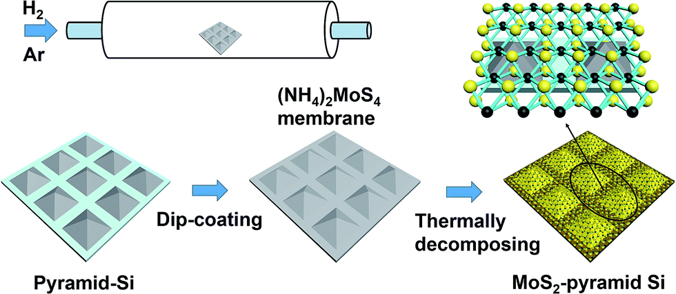 | ||
| Fig. 1 Schematic illustration of the process for the synthesis of MoS2 thin layers on pyramid-Si substrates. The precursor (NH4)2MoS4 was dip-coated on the pyramid-Si substrates. The thermally decomposing process was performed in a quartz tube furnace. | ||
2.2 SERS experiments
SERS experiments were carried out with a Horiba HR Evolution 800 Raman spectrometer with laser wavelength at 532 nm. The excitation laser spot was about 0.5 μm and the incident laser power was kept at 0.5 mW. The laser light was coupled through an objective lens of 50× and the Raman spectra from all substrates were measured under the same conditions. All substrates were immersed in adenosine or cytidine solution with different concentrations for 2 h at 25 °C, washed with deionized water and dried to obtain the enhanced Raman spectra. SERS measurements were taken from at least five random points that were more than 2 mm apart. If there is no special instruction, the mentioned Raman spectra are expressed in terms of average spectra.2.3 Apparatus and characterization
The surface morphology of the MoS2-pyramids-Si substrate was characterized by SEM (SEM, Zeiss Gemini Ultra-55) and AFM (Park XE-100) in the noncontact mode. The crystallinity of MoS2 layers were characterized by XRD (Rigaku D/MAX-RB). The Raman spectra of MoS2 film was performed using a Raman spectrometer (Horiba HR-800) with laser excitation at 532 nm (2.33 eV).3. Results and discussion
The surface morphology of three different kinds of as-grown MoS2 layers were evaluated by SEM image. As illustrated in the SEM images in Fig. 2(a), the MoS2-flat-Si substrate presents a uniform color and smooth surface. In order to clearly observe the surface morphology, SEM image under a high magnification was obtained, as shown in Fig. 2(b). There are continuous cracks and few particles on the surface of the MoS2-flat-Si substrate, indicating that uniform and complanate MoS2 layers have complete synthetized on the flat-Si substrate. Fig. 2(c) shows the surface morphology of the pyramid-Si substrate, these regular pyramids array is relatively uniform on the pyramid-Si substrate. The average height of pyramids is 3 μm and the average distance is 4 μm and this porous structure can effectively improve the MoS2 layers formation and SRES sensitivity. Fig. 2(c)–(e) are SEM images of the MoS2-pyramid-Si substrate in different magnification. After MoS2 layers synthetized on the pyramid-Si substrate, the substrate exhibits a darker and non-specular surface compare to the substrate without MoS2 synthetized in Fig. 2(c). SEM images of the MoS2-pyramid-Si substrate under a high magnification are shown in Fig. 2(d) and (e). Obviously, the MoS2 thin layers almost completely covered the pyramid-Si substrate. There are few micropores on the surface of MoS2-pyramid-Si substrate probably because some tiny bubbles were produced in the dip-coating process. Based on the above SEM images, we preliminary draw a conclusion that the MoS2 layers have successfully synthetized on the flat-Si and pyramid-Si substrate.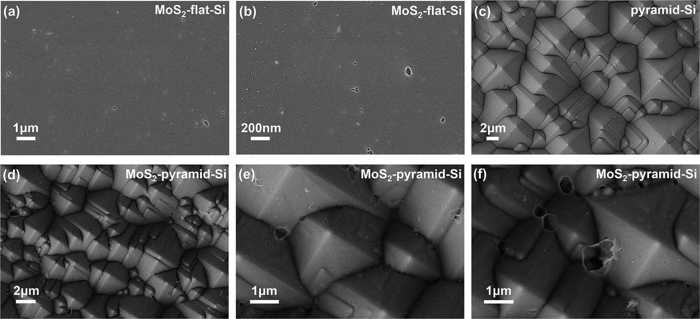 | ||
| Fig. 2 (a) and (b) are SEM images of the MoS2-flat-Si substrate in different magnification. (c) SEM image of the pyramid-Si substrate. (d–f) are SEM images of the MoS2-pyramid-Si substrate in different magnification. | ||
In order to further investigate the characteristics of the as-grown MoS2 layers, Raman spectra were obtained from the randomly selected five points on the MoS2-pyramid-Si (600 °C) substrate, six points on the MoS2-flat-Si substrate, and eight points on the MoS2-pyramid-Si substrate, as shown in Fig. 3(a). For all the Raman spectra obtained from three kinds of substrates, two Raman characteristic peaks of the in-plane E12g and the out-of-plane A1g (at 360–420 cm−1) vibration are all clearly seen.28 It has been reported that the MoS2 structure formed at the thermolysis temperature higher than 300 °C. However, for the MoS2-pyramid-Si (600 °C) substrate, the relatively larger width (∼10 cm−1) of E12g band and weaker intensity (relative to the substrate Si peak at 520 cm−1) indicate that the crystal structure of MoS2 is still not perfect. Note that the second annealing can effectively promote MoS2 formation and sulfur source can effectively supply the sulfur vacancy. For MoS2-flat-Si substrate and MoS2-pyramid-Si substrate, the full-width-half-maximum (FWHM) values of E12g and A1g band respectively are 6–7 and 3–4 cm−1, and the stable Raman characteristic peaks indicate that the uniform MoS2 layers have successfully synthesized. The relatively narrow and strong of E12g mode, which suggest the high quality of MoS2 crystal structure. The peak frequency difference (Δ) between E12g and A1g bands can be used to identify the layer number of MoS2.28 The value of Δ between E12g and A1g bands obtained from the randomly selected eight points on the MoS2-pyramid-Si substrate and six points on the MoS2-flat-Si substrate are shown in Fig. 3(b). The eight points on the MoS2-pyramid-Si substrate are marked with black color and the values of Δ are all in a range of 23–25 cm−1, which indicate that the as-grown MoS2 are 3–5 layers. The MoS2-flat-Si substrate are similar to the MoS2-pyramid-Si substrate with 3–6 layers. In order to further certify the coverage rate of MoS2 layers, Raman mapping of E12g band was obtained from the MoS2-pyramid-Si substrate in an area of 10 × 10 μm2. The blue point in Fig. 3(c) corresponds to the Raman spectra marked with blue curve in Fig. 3(a). The Raman intensity of E12g band is in a range of 480–530 (the baseline is ∼350), which indicate that the pyramid-Si substrate is almost covered with MoS2 layers. Fig. 3(d) and (e) show EDS spectra from the MoS2-pyramid-Si substrate and MoS2-flat-Si substrate, respectively. The peaks associated to silicon element are clearly observed. The molybdenum and sulfur related peaks are very weak, possible due to the ultrathin structure of MoS2 layers. The AFM images of the MoS2-pyramid-Si substrate was also performed, as shown in Fig. 4(a). From the AFM image in a large-scale, one can see that the surface of the pyramid-Si array is smooth. In order to observe more clearly, a magnified AFM image was obtained, as shown in top right corner inset in Fig. 4(a). The holes marked with blue circles are correspond to the micropores in SEM images and the depth is ∼3 nm (the thickness of the monolayer MoS2 is ∼0.7 nm). Fig. 4(d) shows the X-ray diffraction (XRD) pattern of the MoS2-pyramid-Si substrate, there are three pronounced peaks at 2θ = 31.910°, 69.016° and 69.158° assigned as the (100), (200) and (108) reflections, respectively [powder diffraction file (PDF) no. 751539]. The (002) peak can hardly be detected, which indicate that the as-grown MoS2 is in a structure of monolayer or few layers.29,30
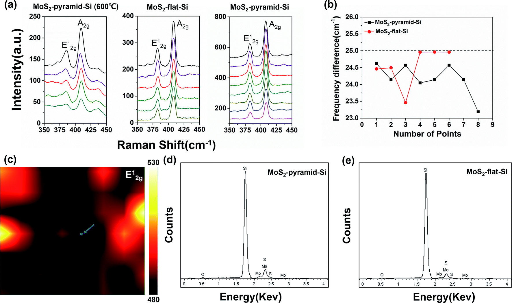 | ||
| Fig. 3 (a) Raman spectra of the random points obtained from the MoS2-pyramid-Si (600 °C), MoS2-flat-Si, and MoS2-pyramid-Si substrate. (b) The calculated peak frequency difference (Δ) between E12g and A1g Raman modes according to the Raman spectra in (a). (c) Raman mapping for the E12g band obtained from an area of 10 × 10 μm2. (d) EDS spectra of the MoS2-pyramid-Si substrate. (d) EDS spectra of the MoS2-flat-Si substrate. | ||
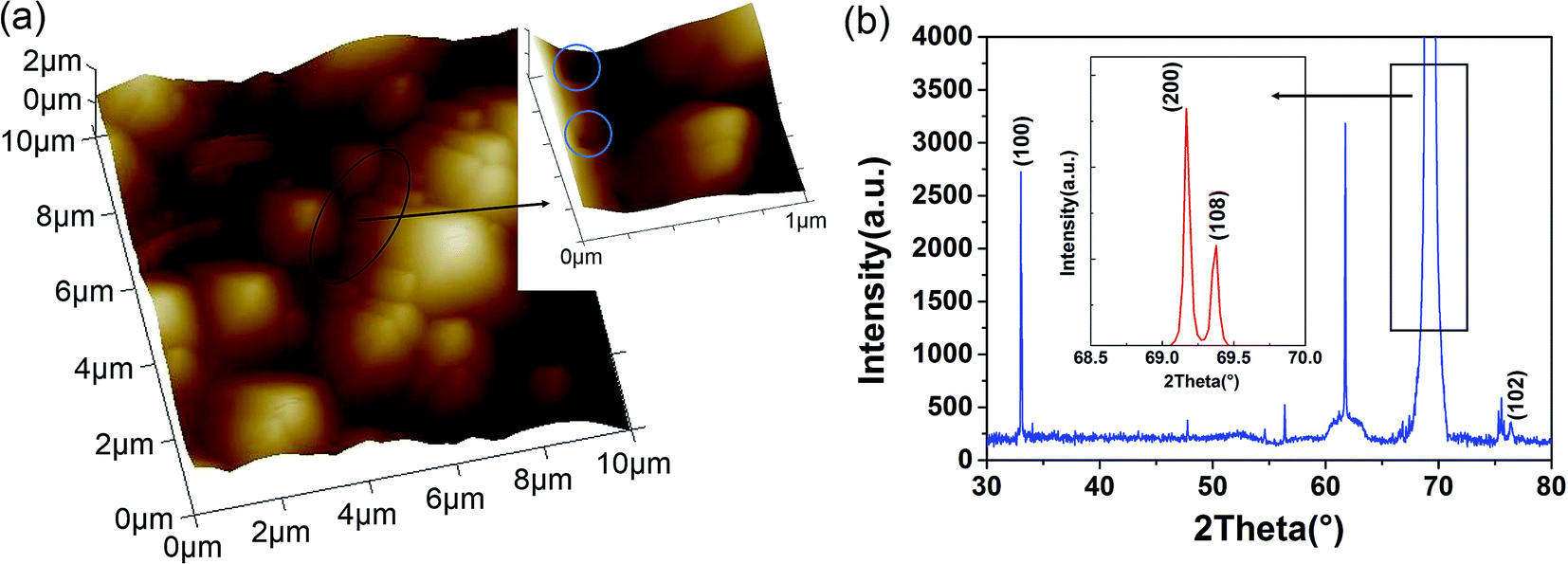 | ||
| Fig. 4 (a) AFM image of the MoS2-pyramid-Si substrate. (b) XRD pattern of the MoS2-pyramid-Si substrate. | ||
Adenosine was selected as the probe molecule to demonstrate the SERS effect of the three kinds of substrate. The characteristic Raman peaks of adenosine have confirmed according to the previous works.31,32 The peaks at 725 and 1576 cm−1 assigned to the ring breathing modes of the whole molecule. The peak at 841 cm−1 assigned to skeletal mode of C–O–C. The peak at 1301 cm−1 assigned to the stretching vibration of N–C–N and C–C–N. The peak at 1330 cm−1 assigned to the stretching vibration of C–N and the bending vibration of C–H. The peak at 1370 cm−1 assigned to the bending vibration of N–H and C–H. For all the SERS substrates, the measured Raman intensity decay with the decrease of the adenosine concentration. As shown in Fig. 5(a) and (b), the minimum detected concentration of adenosine from MoS2-pyramid-Si substrate is one order of magnitude lower than that from MoS2-flat-Si substrate, which can be as low as 10−6 M. This enhancement effect is almost reached the detection limit of Ag–Si pillar array (adenine of 10−6 M) and Ag–Si pyramid (adenosine of 10−7 M).25,27 The Raman intensity from MoS2-pyramid-Si substrate is 3–5 times stronger than that from MoS2-flat-Si substrate, which can attributed to the well-separated pyramid arrays.33 The pyramid-Si arrays can effectively make the incident laser oscillate between the pyramidal valleys, which will further lead to local enhancement of the incident laser. The scattering area of MoS2-pyramid-Si substrate is relatively larger than MoS2-flat-Si substrate, which can further enhance the scattering cross-section. Fig. 5(c) shows the Raman spectra of adenosine obtained from pyramid-Si substrate and the minimum detected concentration only reached 10−4 M. This phenomenon can be due to the lack of surface plasmons and only this local enhancement of the incident laser can't support the SERS active. Compare the Raman spectra from MoS2-pyramid-Si substrate with that from pyramid-Si substrate, more effective enhancement effect is obvious. The peaks at 718 (725) cm−1 from MoS2-pyramid-Si substrate is ∼13.2 times stronger than that from pyramid-Si substrate. The peaks at 1301 (1297) cm−1 from MoS2-pyramid-Si substrate is ∼15.6 times stronger than that from pyramid-Si substrate. The peaks at 1330 (1339) cm−1 from MoS2-pyramid-Si substrate is ∼13.5 times stronger than that from pyramid-Si substrate. The enhancement factors for other peaks are relatively weaker than the peaks above mentioned. From the comparison, the enhancement factors for different peaks are about in a range of 2–15. It should be noted that the multiple of the enhancement, 2–15 times and the vibration dependence of the enhancement factors are both consistent with the chemical enhancement mechanism. Moreover, for pyramid-Si substrate with the concentration of 10−4 M, some Raman peaks can't be distinguished because of the merger phenomena, such as the peaks at 725 and 755 cm−1, which indicates that MoS2 layers can contribute to the peak identification. The Raman peaks from MoS2-pyramid-Si substrate appear little red shift or blue shift compare with that from pyramid-Si substrate, which is because the chemical interaction of charge transfer and dipole–dipole coupling. The peaks at 718 and 1330 cm−1 were selected to investigate the relationship between the Raman intensity and the concentrations. Fig. 5(d) shows the Raman intensity as a function of the adenosine concentrations. To represent the capability of the quantitative detection of adenosine, the linear fit calibration curve (R2) with error bars is presented and the value of R2 of 718 and 1330 cm−1 can reach 0.941 and 0.988, respectively. The excellent linear response between the Raman intensity and adenosine concentrations prove that the prepared MoS2-pyramid-Si substrate can serve as good SERS substrate for nucleoside detection.
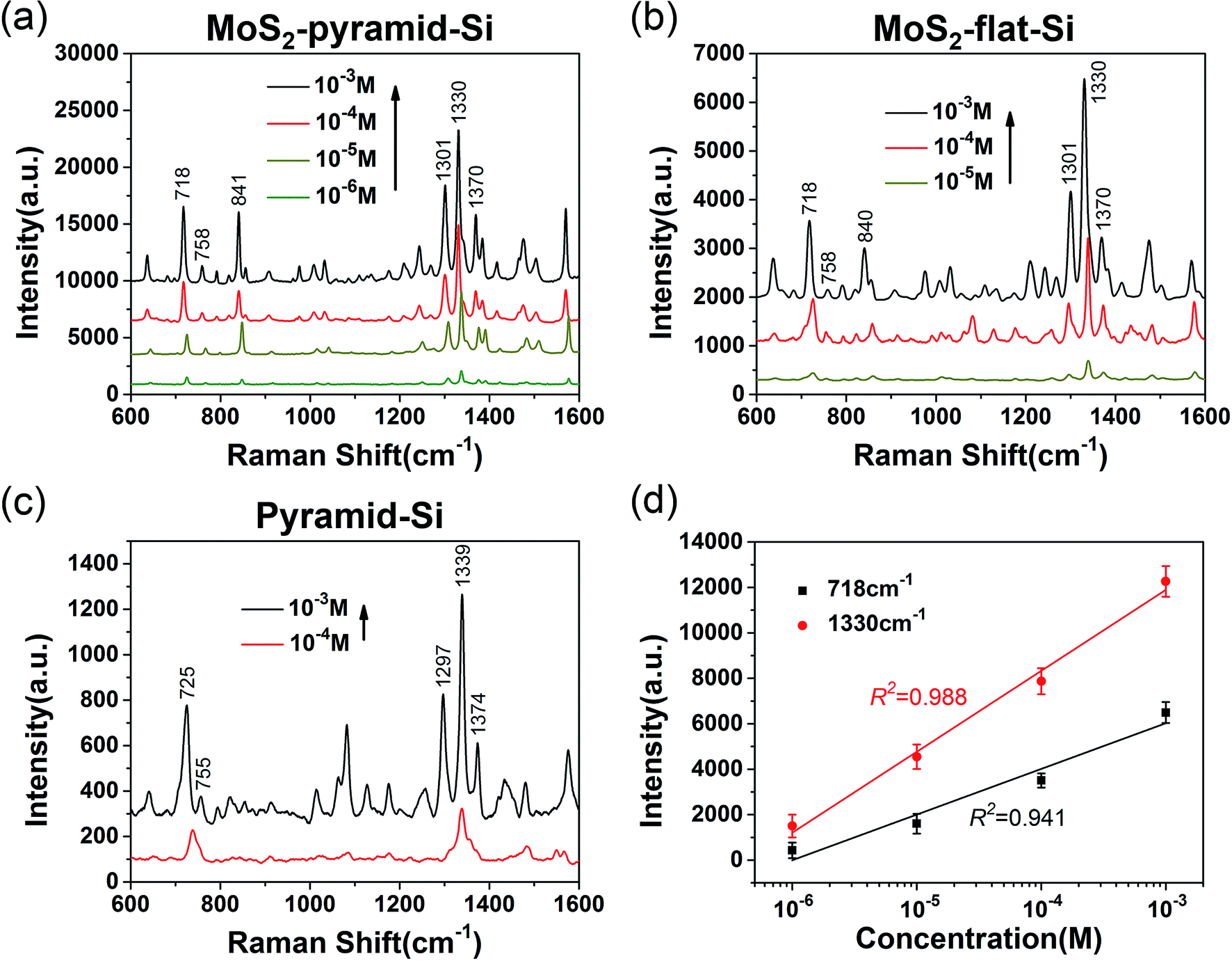 | ||
| Fig. 5 (a) The Raman spectra of adenosine on the MoS2-pyramid-Si substrate from 10−3 to 10−6 M. (b) The Raman spectra of adenosine on the MoS2-flat-Si substrate from 10−3 to 10−5 M. (c) The Raman spectra of adenosine on the pyramid-Si substrate from 10−3 to 10−4 M. (d) Raman intensity of adenosine on the MoS2-pyramid-Si substrate at 718 and 1330 cm−1 as a function of concentration. | ||
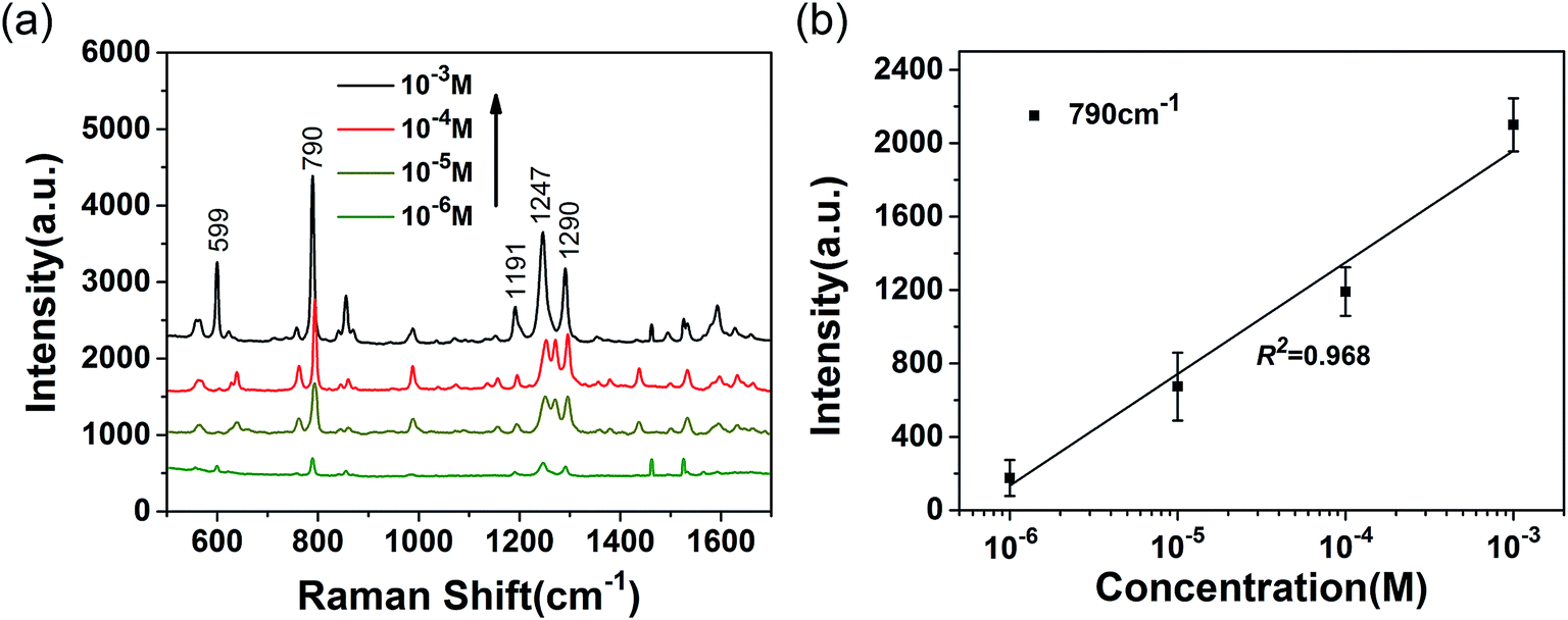
In order to further demonstrate the feasibility of the prepared SERS substrate for nucleoside detection, another nucleoside molecule was selected in experiment, which is cytidine. As shown in Fig. 6(a), all the Raman peaks are inosculate with the reported work.34,35 The peak at 599 cm−1 assigned to the deformation ring. The peak at 790 cm−1 assigned to the ring breathing. The peaks at 1247 and 1290 cm−1 assigned to stretching vibration of C–N and bending vibration of N–H and C–H. There are different enhancement effect of each Raman peak due to the different adsorption states, such as the peak at 599 cm−1 is noticeable for concentration of 10−3 M and negligible for concentration of 10−4–10−6 M. The peak at 1270 cm−1 is just opposite with the peak at 599 cm−1. The Raman intensity of the peaks at 790 cm−1 shows the close relationship with the concentrations of cytidine, which was selected to further study the enhancement effect. Fig. 6(b) shows the reasonable linear response between the Raman intensity and the concentration of cytidine, the value of R2 is reached 0.968, which indicates the as-grown MoS2-pyramid-Si substrate is an effective platform for the SERS molecular detection. The MoS2 layers cover metal nanoparticles may have better Raman enhancement effect, further studies are now in progress in our group.
 | ||
| Fig. 6 (a) The Raman spectra of cytidine on the pyramid-Si substrate from 10−3 to 10−6 M. (b) Raman intensity of cytidine on the MoS2-pyramid-Si substrate at 790 cm−1 as a function of concentration. | ||
4. Conclusions
We have successfully synthesized MoS2 thin layers on the pyramid-Si substrate for SERS detection. Two different nucleoside molecules (adenosine and cytidine) were selected to investigate the SERS ability of the papered substrate, show that the MoS2-pyramid-Si substrate possesses excellent Raman enhancement effect. The minimum detected concentration of both adenosine and cytidine can be as low as 10−6 M, which can be attributed to the biological compatibility and chemical enhancement of MoS2. This MoS2-pyramid-Si substrate may provide a new way toward practical applications for the ultrasensitive and label-free SERS detection of biomolecule. The combination of MoS2 and metal nanoparticles is now in progress in our group.Acknowledgements
The authors are grateful for financial support from the National Natural Science Foundation of China (61205174, 61401258, 11404193, and 11474187), Shandong Province Natural Science Foundation (ZR2013HL049, ZR2013EMM009, and ZR2014FQ032), and Excellent Young Scholars Research Fund of Shandong Normal University.References
- S. Nie and S. R. Emory, Science, 1997, 275, 1102–1106 CrossRef CAS PubMed.
- A. Barhoumi and N. J. Halas, J. Am. Chem. Soc., 2010, 132, 12792–12793 CrossRef CAS PubMed.
- K. Lee, V. P. Drachev and J. Irudayaraj, ACS Nano, 2011, 5, 2109–2117 CrossRef CAS PubMed.
- X. Ling, L. M. Xie, Y. Fang, H. Xu, H. L. Zhang, J. Kong, M. S. Dresselhaus, J. Zhang and Z. F. Liu, Nano Lett., 2010, 10, 553–561 CrossRef CAS PubMed.
- Y. M. Liu, Y. Hu and J. Zhang, J. Phys. Chem. C, 2014, 118, 8993–8998 CAS.
- J. Zheng, X. Li, R. Gu and T. Lu, J. Phys. Chem. B, 2002, 106, 1019–1023 CrossRef CAS.
- Y. G. Li, H. L. Wang, L. M. Xie, Y. Y. Liang, G. S. Hong and H. J. Dai, J. Am. Chem. Soc., 2011, 133, 7296–7299 CrossRef CAS PubMed.
- B. Radisavljevic, A. Radenovic, J. Brivio, V. Giacometti and A. Kis, Nat. Nanotechnol., 2011, 6, 147–150 CrossRef CAS PubMed.
- J. Xiao, D. Choi, L. Cosimbescu, P. Koech, J. Liu and J. P. Lemmon, Chem. Mater., 2010, 22, 4522–4524 CrossRef CAS.
- H. Hwang, H. Kim and J. Cho, Nano Lett., 2011, 11, 4826–4830 CrossRef CAS PubMed.
- L. F. Sun, J. X. Yan, D. Zhan, L. Liu, H. L. Hu, H. Li, B. K. Tay, J. L. Kuo, C. C. Huang, D. W. Hewak, P. S. Lee and Z. X. Shen, Phys. Rev. Lett., 2013, 111, 126801 CrossRef.
- H. Wang, L. L. Yu, Y. H. Lee, Y. M. Shi, A. Hsu, M. L. Chin, L. J. Li, M. Dubey, J. Kong and T. Palacios, Nano Lett., 2012, 12, 4674–4680 CrossRef CAS PubMed.
- Q. J. Xiang, J. G. Yu and M. Jaroniec, J. Am. Chem. Soc., 2012, 134, 6575–6578 CrossRef CAS PubMed.
- J. L. Verble and T. J. Wieting, Phys. Rev. Lett., 1970, 25, 362–365 CrossRef CAS.
- X. Ling, W. J. Fang, Y. H. Lee, P. T. Araujo, X. Zhang, J. F. Rodriguez-Nieva, Y. X. Lin, J. Zhang, J. Kong and M. S. Dresselhaus, Nano Lett., 2014, 14, 3033–3040 CrossRef CAS PubMed.
- P. Wang, O. Liang, W. Zhang, T. Schroeder and Y. H. Xie, Adv. Mater., 2013, 25, 4918–4924 CrossRef CAS PubMed.
- W. G. Xu, J. Q. Xiao, Y. F. Chen, Y. B. Chen, X. Ling and J. Zhang, Adv. Mater., 2013, 25, 928–933 CrossRef CAS PubMed.
- Y. W. Zhang, S. Liu, L. Wang, X. Y. Qin, J. Q. Tian, W. B. Lu, G. H. Chang and X. P. Sun, RSC Adv., 2012, 2, 538–545 RSC.
- S. C. Xu, B. Y. Man, S. Z. Jiang, J. H. Wang, J. Wei, S. D. Xu, H. P. Liu, S. B. Gao, H. L. Liu, Z. H. Li, H. S. Li and H. W. Qiu, ACS Appl. Mater. Interfaces, 2015, 7, 10977–10987 CAS.
- A. Chiolerio, A. Virga, P. Pandolfi, P. Martino, P. Rivolo, F. Geobaldo and F. Giorgis, Nanoscale Res. Lett., 2012, 7, 1–7 CrossRef PubMed.
- Y. Q. Wang, S. Ma, Q. Q. Yang and X. J. Li, Appl. Surf. Sci., 2012, 258, 5881–5885 CrossRef CAS PubMed.
- B. Kiraly, S. Yang and T. J. Huang, Nanotechnology, 2013, 24, 245704 CrossRef PubMed.
- X. Sun, N. Wang and H. Li, Appl. Surf. Sci., 2013, 284, 549–555 CrossRef CAS PubMed.
- J. Q. Li, C. Chen, H. Jans, X. M. Xu, N. Verellen, I. Vos, Y. Okumura, V. V. Moshchalkov, L. Lagaea and P. V. Dorpe, Nanoscale, 2014, 6, 12391–12396 RSC.
- F. Feng, G. Zhi, H. S. Jia, L. Cheng, Y. T. Tian and X. J. Li, Nanotechnology, 2009, 20, 295501 CrossRef PubMed.
- R. R. Juluri, A. Rath, A. Ghosh, A. Bhukta, R. Sathyavathi, D. N. Rao, K. Muller, M. Schowalter, K. Frank, T. Grieb, F. Krause, A. Rosenauer and P. V. Satyam, Sci. Rep., 2014, 4, 4633 CAS.
- C. Zhang, B. Y. Man, S. Z. Jiang, C. Yang, M. Liu, C. S. Chen, S. C. Xu, H. W. Qiu and Z. Li, Appl. Surf. Sci., 2015, 347, 668–672 CrossRef CAS PubMed.
- C. Lee, H. Yan, L. E. Brus, T. F. Heinz, J. Hone and S. Ryu, ACS Nano, 2010, 4, 2695–2700 CrossRef CAS PubMed.
- K. F. Mak, C. Lee, J. Hone, J. Shan and T. F. Heinz, Phys. Rev. Lett., 2010, 105, 136805 CrossRef.
- H. S. S. Ramakrishna Matte, A. Gomathi, A. K. Manna, D. J. Late, R. Datta, S. K. Pati and C. N. R. Rao, Angew. Chem., Int. Ed., 2010, 49, 4059–4062 CrossRef PubMed.
- B. Giese and D. McNaughton, J. Phys. Chem. B, 2002, 106, 101–112 CrossRef CAS.
- J. Li and Y. Fang, Spectrochim. Acta, Part A, 2007, 66, 994–1000 CrossRef PubMed.
- C. Zhang, S. Z. Jiang, Y. Y. Huo, A. H. Liu, S. C. Xu, X. Y. Liu, Z. C. Sun, Y. Y. Xu, Z. Li and B. Y. Man, Opt. Express, 2015, 23, 24811–24821 CrossRef CAS PubMed.
- J. S. Suh and M. Moskovit, J. Am. Chem. Soc., 1986, 108, 4711–4718 CrossRef CAS.
- S. Mansya, W. L. Peticolasa and R. S. Tobias, Spectrochim. Acta, Part A, 1979, 35, 315–329 CrossRef.
| This journal is © The Royal Society of Chemistry 2015 |