
Graphene stabilized high-κ dielectric Y2O3 (111) monolayers and their interfacial properties
Ting Ting Songa,
Ming Yang*b,
Martin Callsenc,
Qing Yun Wuc,
Jun Zhouc,
Shao Feng Wanga,
Shi Jie Wangb and
Yuan Ping Feng*c
aInstitute for Structure and Function and Department of Physics, Chongqing University, Chongqing, 400044, People’s Republic of China
bInstitute of Materials Research and Engineering, 3 Research Link, 117602, Singapore. E-mail: yangm@imre.a-star.edu.sg
cDepartment of Physics, National University of Singapore, 2 Science Drive 3, 117542, Singapore. E-mail: phyfyp@nus.edu.sg
First published on 16th September 2015
Abstract
The exfoliation of graphene triggered dramatic interest to explore other two-dimensional materials for functionalizing future nanoelectronic devices. In this study, via first-principles calculations, we predict a stable planar Y2O3 (111) monolayer with a direct band gap of 3.96 eV. This high-κ dielectric monolayer can be further stabilized by a graphene substrate. The interaction between the planar Y2O3 (111) monolayer and graphene is found to be weak and dominated by van der Waals interactions, while the electronic properties are determined by orbital hybridization and electrostatic interaction. Our results indicate that a high-κ dielectric monolayer can be formed on a substrate with weak interfacial interaction via a physical deposition process, and this sheds light on engineering extremely thin high-κ dielectrics on graphene-based electronics with desired properties.
1 Introduction
In the past decades, the performance of silicon (Si) based field-effect transistors (FETs) has been improved dramatically by scaling technology. Due to the relatively small dielectric constant of SiO2, the thickness of this gate dielectric is now approaching its physical limit. In order to further improve the performance of FETs, high-κ dielectrics such as HfO2 have replaced conventional gate dielectric SiO2, due to its much larger dielectric constant.1,2 On the other hand, tremendous efforts have also been made to find a channel material with high carrier mobility to substitute Si, of which graphene, a monolayer of carbon atoms with honeycomb lattices, has been a focus in recent years.3–5 Graphene has many fascinating mechanical, optical, and electronic properties. One of the interesting properties of graphene is its high intrinsic carrier mobility which is highly desirable for future high speed electronic devices.6 It has been reported that the electron mobility of free standing graphene is up to 200![[thin space (1/6-em)]](https://www.rsc.org/images/entities/char_2009.gif) 000 cm2 V−1 s−1 at room temperature.7 Integrating high-κ dielectrics into graphene based electric devices takes advantage of both materials. The interface between graphene and the high-κ oxide is expected to play a crucial role in the performance of such devices.8 However, the graphene/high-κ dielectrics interface is different from that of the Si/high-κ dielectrics interface, resulting from the inert surface of graphene. Extensive studies have been carried out to understand the interfacial interaction between graphene and high-κ dielectrics. It is found that the interaction between graphene and high-κ dielectrics strongly depends on the surface chemical environment of the dielectrics.9–14 Experimentally, various high-κ dielectrics have been grown on graphene, including HfO2,15 Al2O3,8 ZrO2,16 Si3N4,17–19 and Y2O3 (ref. 20 and 21) thin films or nanoribbons. The electric properties of these graphene/high-κ dielectric devices have been much improved compared to SiO2, because high-κ dielectrics can increase capacitance density significantly and also screen the scattering of interfacial charged impurities effectively.
000 cm2 V−1 s−1 at room temperature.7 Integrating high-κ dielectrics into graphene based electric devices takes advantage of both materials. The interface between graphene and the high-κ oxide is expected to play a crucial role in the performance of such devices.8 However, the graphene/high-κ dielectrics interface is different from that of the Si/high-κ dielectrics interface, resulting from the inert surface of graphene. Extensive studies have been carried out to understand the interfacial interaction between graphene and high-κ dielectrics. It is found that the interaction between graphene and high-κ dielectrics strongly depends on the surface chemical environment of the dielectrics.9–14 Experimentally, various high-κ dielectrics have been grown on graphene, including HfO2,15 Al2O3,8 ZrO2,16 Si3N4,17–19 and Y2O3 (ref. 20 and 21) thin films or nanoribbons. The electric properties of these graphene/high-κ dielectric devices have been much improved compared to SiO2, because high-κ dielectrics can increase capacitance density significantly and also screen the scattering of interfacial charged impurities effectively.
Following graphene, many other two-dimensional materials have been found, which include graphene like silicene,22 h-BN,3 transition metal dichalcogenides such as MoS2,3 black phosphorene,23,24 as well as III–V and II–VI materials.25–30 More recently, a crystalline double-layer SiO2 sheet has been deposited on a Ru (0001) substrate.31 It is noted that when the thickness of dielectric thin films is reduced, the interaction between graphene and the dielectric might be changed accordingly. For example, for graphene adsorbed on the Al2O3 (0001) surface, the interaction between them is found to be strong,12 while in contrast, a weak interaction is found at the interface between graphene and the Y2O3 (111) monolayer.32 In addition, graphene has been assembled on a single layer of h-BN, and the interaction between them is dominated by the van der Waals (vdW) force.33 These results indicate that both the surface chemical environment and the thickness of dielectrics might play an important role in determining the interaction between graphene and dielectrics, and motivate us to study the stability of a high-κ oxide dielectric monolayer and its interfacial properties with graphene. In this study, based on first-principles calculations, we find that a free standing planar Y2O3 (111) monolayer is stable, and its stability can be further enhanced when it is supported by graphene. In addition, the interfacial interaction between them is weak, with the main contribution arising from vdW interaction, while the electronic properties are mainly determined by electrostatic interactions and orbital hybridization between C pz and O pz, as well as C pz and Y 4d orbitals.
2 Methodology
All calculations were carried out using density-functional theory (DFT) as implemented in VASP code.34,35 Generalized gradient approximation (GGA) in the form of Perdew–Burke–Ernzerhof (PBE) was used for the exchange–correlation functional, and the projector augmented wave (PAW) potentials were selected to describe the interaction between electrons and ions.36 The cutoff energy for the plane wave expansion was set to 500 eV. Γ centered 18 × 18 × 1 and 4 × 4 × 4 κ-point meshes were used to sample the first Brillouin zone of pristine graphene and Y2O3 bulk, and 9 × 9 × 1 κ-point meshes were applied for the Y2O3 (111) monolayer, Y2O3 (111) monolayer on graphene, and Y2O3 (111) monolayer on Y (0001) surface, respectively. To minimize the interaction between image surfaces, a 15 Å vacuum was normally applied to the Y2O3 surface for all interface structures. Corrections for vdW effects were included in the calculations by using Grimme’s DFT-D2 method with C6 (1.75, 0.70, and 24.67) and R0 (1.452, 1.342, and 1.639) for C, O, and Y atoms, respectively. The DFT-D2 calculation results were partially compared with the results by the self-consistent ab initio van der Waals density-functional (vdW-DF) method.37,38 All structures were optimized until the residual force on each atom is smaller than 0.01 eV Å−1. For the electronic structure of the Y2O3 monolayer, Heyd–Scuseria–Ernzerhof hybrid functionals (HSE06) were used.39 To examine the thermal stability of the Y2O3 (111) monolayer, ab initio molecular dynamics simulations were performed with a time step of 1 fs, canonical ensemble (NVT), and Nosé heat bath. In addition, phonon dispersion was calculated using density functional perturbation theory implemented in VASP with a higher electronic convergence criterion of 10−8 eV and analyzed by using the PHONOPY code.40 Based on these settings, the calculated lattice constant and PBE band gap of Y2O3 bulk are 10.51 Å and 4.5 eV, respectively, which is in good agreement with previous results.413 Results and discussions
The clean Y2O3 (111) surface is polar, terminated by O atoms, which is unstable, and structural relaxation or even reconstruction is needed to suppress surface polarization.44 Particularly when the thickness of Y2O3 (111) thin films approach their physical limit one monolayer, the Y2O3 (111) single layer, may undergo structural reconstruction. The reconstructed Y2O3 (111) monolayer shown in Fig. 1(a) is a hexagonal planar structure with 3 O atoms and 2 Y atoms in the unit cell with a lattice constant of 7.22 Å. It is noted that the planar form is the energetically most stable for Y2O3 (111) and its total energy is about 0.6 eV per atom lower than that of a buckled structure. The Y–O bond length in the Y2O3 (111) monolayer is 2.08 Å, about 0.2 Å smaller than that in bulk Y2O3, indicating stronger in-plane bonding in monolayer Y2O3 due to reduced coordinations.43 The suppression of surface polarization in this planar Y2O3 (111) monolayer also leads to an enhanced in-plane covalent bonding character, because the calculated Bader charges suggest an ionic formula of Y2+1.95O3−1.3, less than Y2+2.16O3−1.44 in bulk form.42 Fig. 1(b) is the calculated phonon spectra of the planar Y2O3 (111) monolayer. No imaginary frequency has been found, indicating that the planar Y2O3 (111) monolayer is dynamically stable. The stability of this monolayer is further confirmed by the MD simulation results, as shown in Fig. 1(c) and (d). The Y–O bond displacement is within 0.18 Å at the simulated temperature of 300 K during the 10 ps MD simulation. The configuration of the Y2O3 monolayer supercell at the maximum bond displacement (about 0.18 Å) is shown in Fig. 1(e) and (f). It can be seen that only a slight distortion is found in the Y2O3 monolayer at room temperature.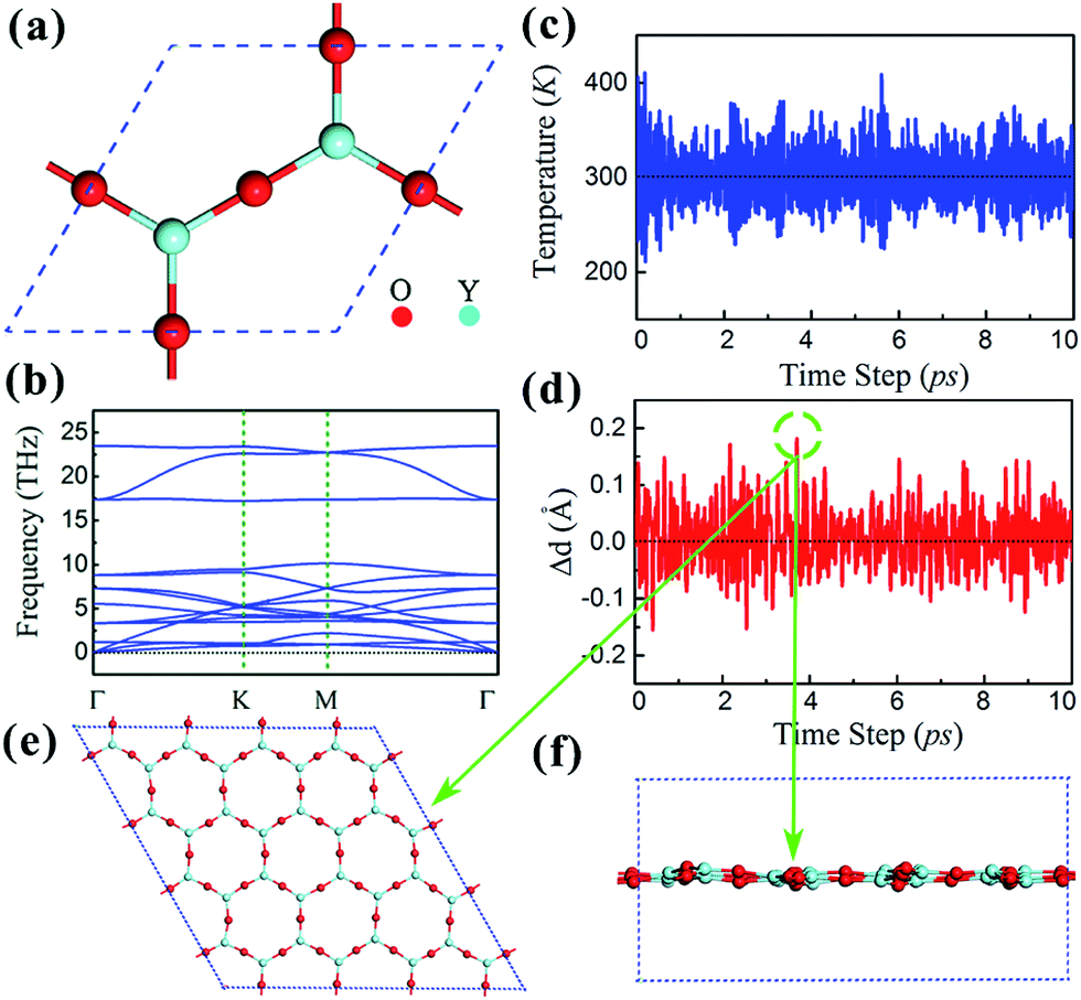 | ||
| Fig. 1 (a) Top view of the planar Y2O3 (111) monolayer. (b) Phonon dispersion of the planar Y2O3 (111) monolayer. The temperature evolution (c) and the evolution of Y–O bond (d) during the 10 ps MD simulation at room temperature, in which the bond displacement Δd is defined as the difference between the Y–O bond length in MD simulations (d) and its equilibrium bond length (d0). The top view (e) and side view (f) for the Y2O3 (111) monolayer with the maximum bond displacement during the 10 ps MD simulation. | ||
The electronic and dielectric properties of the planar Y2O3 (111) monolayer are shown in Fig. 2. From the calculated HSE06 band structure (Fig. 2(a)), both the valence band maximum and conduction band minimum are located at the Γ point, suggesting a direct band gap of 3.96 eV. This band gap is smaller than that of bulk Y2O3 due to different bonding characters. The corresponding total and projected density of states (DOS) are presented in Fig. 2(b), in which the flat valence band maximum is mainly derived from the 2p orbital of O atoms, weakly hybridized with a 4d orbital of Y atoms, forming σ bonds. For the lower valence bands (−1.4 eV to −0.8 eV), the formation of π bonds is found, as pz orbitals of O atoms and t2g orbitals of Y atoms hybridize to each other, which favors the formation of a planar two-dimensional structure.26 The calculated dielectric function of this planar Y2O3 (111) monolayer is presented in Fig. 2(c). The static dielectric constant of the Y2O3 (111) monolayer is 1.5. It is noted that only the electronic contributions were included in the calculations. Even taking into account other effects such as ionic and dipolar contributions, the calculated dielectric constant of the Y2O3 (111) monolayer is still smaller than that of the Y2O3 bulk due to the reduced thickness and dimensionality.41
 | ||
| Fig. 2 (a) Band structure (b) total and projected DOS of the planar Y2O3 (111) monolayer. (c) Dielectric function of the Y2O3 monolayer. The Fermi energy is shifted to 0 eV. | ||
One possible way for the growth of the Y2O3 (111) monolayer is to deposit Y2O3 thin films on a substrate. Thus, it is crucial to understand the interaction between the planar Y2O3 monolayer and the substrate. Next, we examine the stability and interfacial properties of the planar Y2O3 (111) monolayer supported on substrates. In this study, graphene is selected as the substrate, as the Y2O3 (111) monolayer has been deposited on graphene.32 To model the planar Y2O3 (111) monolayer/graphene hybrid interface structure, 2.2% tensile strain is applied on the planar Y2O3 (111) monolayer to match a 3 × 3 × 1 graphene supercell, as shown in Fig. 3(a). The small strain reduces the band gap of the planar Y2O3 (111) monolayer by about 0.04 eV, but does not change the orbital characters of the valence band and conduction band. The most stable interfacial configuration (see Fig. 3(a)) is such that the Y atom of the planar Y2O3 monolayer is directly above the C ring center and O atom is at the bridge site of the C–C bond, similar to interfacial configurations of graphene on SiO2 and Si3N4.9,18 The interface formation energy is minimized through maximizing the potential local bonding. When supported on graphene, the planar Y2O3 (111) monolayer becomes more stable and its energy is lowered by 0.46 eV per atom. In the relaxed structure, Y atoms slightly moved out of the Y2O3 plane by about 0.05 Å, toward to the graphene plane slightly, resulting in a longer Y–O bond length of 2.11 Å and slightly buckled Y2O3 layer, compared with that of the free standing planar Y2O3 (111) monolayer. The calculated Y–O bond length is close to the experimental result (2.25 Å), but the Y–Y distance (4.17 Å) is much larger.32 We also study the structural stability of the planar Y2O3 (111) monolayer/graphene at a high temperature. From the results of our MD simulation of Y2O3 (111) monolayer/graphene carried out at 850 K shown in Fig. 3(d) and (e), we can see that the Y2O3 monolayer remains stable on graphene at this temperature, but its structural distortion is much more pronounced. The maximum displacement of the Y–Y distance is about 0.8 Å. This indicates that the Y2O3 monolayer tends to buckle at a high temperature as observed in a recent experiment.32
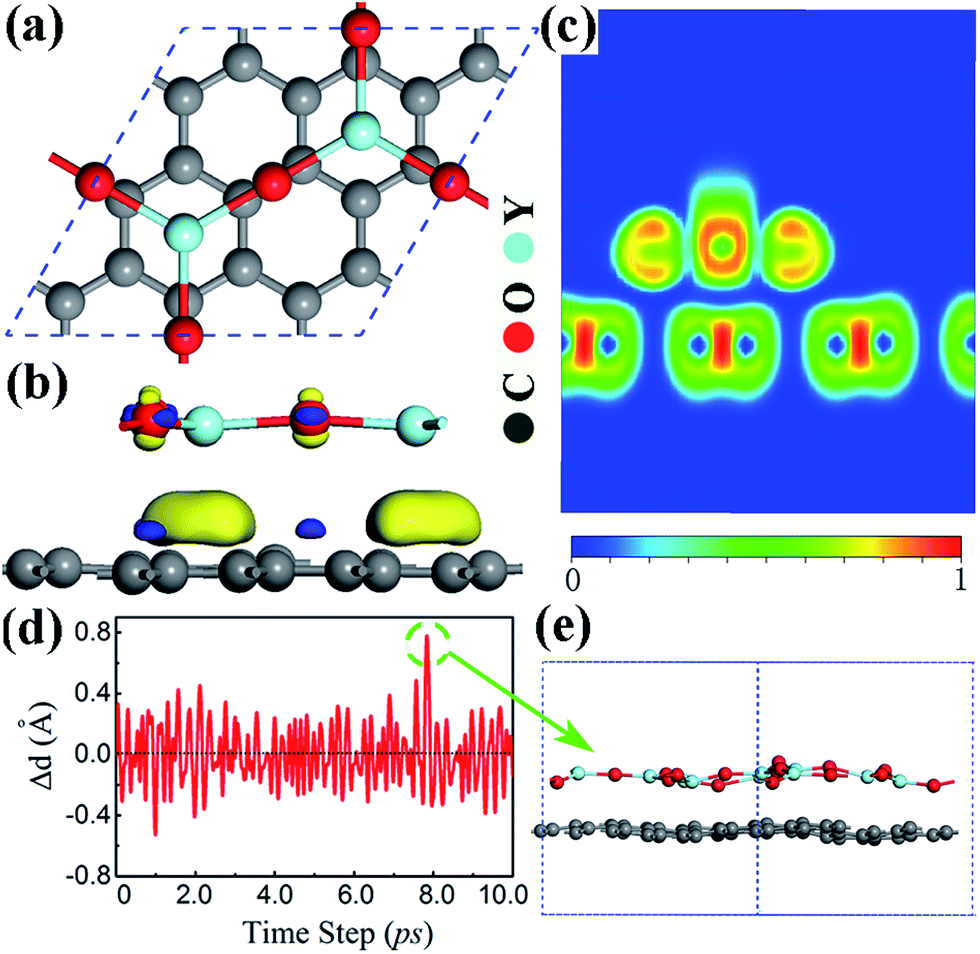 | ||
| Fig. 3 (a) Top view of the planar Y2O3 (111) monolayer on the (3 × 3 × 1) graphene. (b) Side view of charge density difference between the Y2O3 (111) monolayer and graphene, where the charge density difference (Δp) is defined by Δp = ρ(G+Y2O3) − ρG − ρY2O3, and visualized with an isosurface value of 1.0 × 1.0−3 eV Å−3. Yellow color denotes excess charge density and blue color denotes depleted charge density. (c) Contour plot of the ELF for the planar Y2O3 (111) monolayer on the graphene along the (110) plane. (d) The evolution of the Y–Y distance for the Y2O3 (111) monolayer on the graphene during 10 ps MD steps at the temperature of 850 K. (e) The side view of the structural configuration with the maximum displacement of the Y–Y distance during the MD simulation. | ||
The DFT-D2 optimized distance between graphene and the planar Y2O3 (111) monolayer is found to be 2.96 Å, which is at the boundary between chemical adsorption and physical adsorption (∼3 Å), but far beyond the covalent bonding range of 1.44 Å for the C–O bond and 2.4 Å for the C–Y bond, respectively. To further investigate the nature of interfacial bonding, the electron localization function (ELF) was calculated.45 Fig. 3(c) shows the ELF in the (110) plane of this stable interfacial configuration. No covalent bonding can be found at the interface between graphene and the planar Y2O3 (111) monolayer. To estimate interfacial interaction strength, we calculated the binding energy which is defined as:
| Eb = EG + EY2O3 − EG+Y2O3, | (1) |
The electronic properties of the planar Y2O3 monolayer on graphene are shown in Fig. 4. From the DFT-D2 calculated band structure (Fig. 4(a)), it is noted that the conduction band minimum that is derived from C pz orbital is about 0.015 eV below the Fermi energy, indicating that the graphene is slightly n-doped. We also found that a gap of about 0.21 eV is open in graphene. Fig. 4(b) is the calculated projected density of states for the Y2O3 (111) monolayer on graphene. Hybridization is found between the O pz and C pz states near the Fermi energy, as well as Y t2g and C pz states. In the energy range of −1 eV to −2 eV, the hybridization between O pz and C pz, and also between C pz and Y eg states are more profound. These orbital hybridizations are further confirmed by the partial charge density at the lower Dirac cone of graphene, where the dominant contribution is from the C pz orbital, but a minor contribution from O atoms is noticeable also, as shown in Fig. 4(c). The origins of gap opening in graphene after integration with the Y2O3 (111) monolayer can be ascribed to structural deformation, or interfacial interaction with Y2O3, or both. To determine which of the above factors play a dominant role, we calculated the band structure of the isolated deformed graphene by removing the planar Y2O3 (111) monolayer. The results show that this deformed graphene does not affect its band structure. Thus, the gap opening in graphene is due to interfacial interaction by the presence of the planar Y2O3 (111) monolayer.
 | ||
| Fig. 4 Electronic structure of the Y2O3 (111) monolayer on graphene. (a) Orbital projected band structure for the planar Y2O3 (111) monolayer on the (3 × 3 × 1) graphene at the DFT-D2 optimized spacing distance of 2.96 Å, in which red solid dots and blue solid lattices denote the contribution from C pz and O p orbitals, respectively. (b) Projected density of states (PDOS) of the C atom in graphene, and its nearest O and Y atom in Y2O3. The inset is showing the magnified PDOS of Y atoms near the Fermi level. (c) Contour plot of partial charge density for the top π orbital in graphene. (d) GGA band structure (without vdW correction) of the planar Y2O3 (111) monolayer on the graphene at the GGA optimized interfacial spacing of 3.60 Å. (e) vdW-DF (optB88 functionals) band structure of the planar Y2O3 (111) monolayer on the graphene at the vdW-DF optimized distance of 3.06 Å. | ||
A number of factors could affect the interfacial interaction between graphene and the planar Y2O3 monolayer, including the interfacial vdW interaction, charge transfer, orbital hybridization, and electrostatic potential interaction. The interfacial charge transfer is not expected to be important for determining the interaction because only about 0.003 electrons per C atom were transferred from Y2O3 to graphene. The effect of vdW interactions can be estimated by comparing the structural and electronic properties of Y2O3 monolayer on graphene with and without the vdW correction. Our calculations show that without the vdW correction the GGA optimized spacing between graphene and the Y2O3 monolayer is significantly increased to 3.6 Å. The band structure of graphene (see Fig. 4(d)) is similar to that of free standing graphene, but with a small gap of 0.04 eV that is due to electrostatic energy difference in graphene AB lattices caused by Y2O3 at this GGA optimized interfacial spacing distance. This shows that vdW interactions play a very important role in determining the spacing distance between graphene and the planar Y2O3 monolayer. Moreover, the effect of vdW interactions on the electronic properties can be seen from the difference between band structures calculated with and without the vdW correction. The band structure in Fig. 4(a) is calculated using the DFT-D2 method, which is a force correction that only affects the structural configuration. In comparison, the band structure in Fig. 4(e) is calculated using the vdW-DF method with the optB88-vdW functional,38 which is a self-consistent vdW correction method, and the vdW interaction effect is included in the band structure calculation. It is noted that these two band structures are nearly identical. These suggest that the vdW interaction binds the Y2O3 monolayer with graphene, but it does not significantly influence its electronic properties.33,47,48 In addition, for the 0.21 eV gap in graphene, about 0.08 eV is ascribed to interfacial electrostatic potential interaction because the electrostatic potential energy difference in graphene AB lattices is about 0.08 eV in the presence of the Y2O3 monolayer.10,12,48 The rest of the contribution should mainly originate from the orbital hybridization as the interfacial charge transfer is very weak and the interfacial vdW interaction does not affect electronic structure. Therefore, orbital hybridization plays an important role in determining electronic properties at the interface of the Y2O3 monolayer/graphene. It is noted that a similar phenomenon has been found at the interface between graphene and Ni, where the adsorption is a typical physisorption, but the electronic structure is mainly determined by orbital hybridization.49 We also studied the interfacial properties of a buckled Y2O3 monolayer on (2 × 2 × 1) graphene. The optimized lattice constant is 5.14 Å, and the calculated Y–Y and Y–O length is about 2.96 and 1.96 Å, respectively. It is also noted that when supported on graphene, the buckled Y2O3 (111) monolayer became much more stable as its energy is dramatically lowered (about 2.7 eV per Y2O3 unit). The Dirac cone of graphene is still preserved in the presence of buckled Y2O3 (see Fig. 5(a) and (b)), but is shifted about 1.1 eV below Fermi energy, in agreement with experimental observations.32
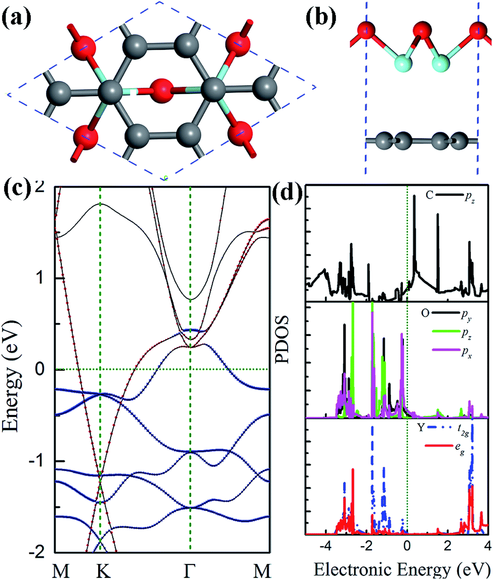 | ||
| Fig. 5 The top (a) and side (b) view of the atomic structure for the Y2O3 (111) monolayer on (2 × 2 × 1) graphene. The corresponding band structure (c) and PDOS (d). | ||
Another possible way to realize the planar Y2O3 (111) monolayer is to oxidize the yttrium (Y) (0001) surface directly. Thus, we further study the interface of the planar Y2O3 (111) monolayer on the Y (0001) substrate. In the most stable structure, the O atoms of the Y2O3 (111) monolayer are on the top of the Y atoms of the yttrium (001) substrate. The interaction between the Y2O3 monolayer and Y is much stronger compared to that between the planar Y2O3 monolayer and graphene, as the interfacial binding energy is as high as 300 meV and the interfacial Y–O bond is formed with a bond length of 2.25 Å, close to the Y–O bonds in bulk Y2O3. The strong interaction also leads to a significant outward relaxation (0.4 Å) of O atoms in the Y2O3 (111) monolayer towards the Y substrate, turning the planar monolayer into a buckled structure. For the two possible methods to grow the Y2O3 monolayer, the direct oxidation method, due to a strong interaction between the Y2O3 and Y substrate as mentioned above, the grown Y2O3 layers tend to be buckled. This is also applied to the physical deposition of Y2O3 on a substrate that has a strong interaction with the Y2O3 layers. In both cases, even though a distorted Y2O3 monolayer can be grown, it is difficult to be exfoliated or transferred for further functionalization as the binding energy between the layers is large. Thus, a more promising method to grow a Y2O3 monolayer is through the physical deposition process on a substrate with a weak interfacial interaction like the planar Y2O3 monolayer on graphene.
4 Conclusions
In conclusion, the results of our first-principles calculations predict a stable Y2O3 (111) monolayer, which has a direct band gap of 3.96 eV. The Y2O3 (111) monolayer can be further stabilized by depositing it on graphene. The weak interaction between the Y2O3 (111) monolayer and graphene indicates that the inert graphene surface is an excellent substrate to grow an Y2O3 (111) two-dimensional monolayer. This growth strategy might be applied to grow other similar high-κ dielectric monolayer on a chemically inert surface. Due to a similar surface chemical nature among graphene and other two-dimensional materials such as MoS2, or black phosphene, our results may shed light on understanding interfacial interactions between two-dimensional materials and other extremely thin high-k oxide films.Acknowledgements
This work was supported by the NUS Academic Research Fund (Grant No. R-144-000-237-133). All calculations were performed at the high performance computing cluster at the Graphene Research Centre of NUS.References
- G. D. Wilk, R. M. Wallace and J. Anthony, J. Appl. Phys., 2001, 89, 5243–5275 CrossRef CAS PubMed.
- J. Robertson, Rep. Prog. Phys., 2006, 69, 327–396 CrossRef CAS.
- K. Novoselov, D. Jiang, F. Schedin, T. Booth, V. Khotkevich, S. Morozov and A. Geim, Proc. Natl. Acad. Sci. U. S. A., 2005, 102, 10451–10453 CrossRef CAS PubMed.
- A. K. Geim and K. S. Novoselov, Nat. Mater., 2007, 6, 183–191 CrossRef CAS PubMed.
- A. C. Neto, F. Guinea, N. Peres, K. S. Novoselov and A. K. Geim, Rev. Mod. Phys., 2009, 81, 109–162 CrossRef.
- K. S. Novoselov, V. I. Falko, L. Colombo, P. R. Gellert, M. G. Schwab and K. Kim, Nature, 2012, 490, 192–200 CrossRef CAS PubMed.
- X. Du, I. Skachko, A. Barker and E. Y. Andrei, Nat. Nanotechnol., 2008, 3, 491–495 CrossRef CAS PubMed.
- L. Liao, J. Bai, Y. Qu, Y.-C. Lin, Y. Li, Y. Huang and X. Duan, Proc. Natl. Acad. Sci. U. S. A., 2010, 107, 6711–6715 CrossRef CAS PubMed.
- Y.-J. Kang, J. Kang and K. Chang, Phys. Rev. B: Condens. Matter Mater. Phys., 2008, 78, 115404 CrossRef.
- N. T. Cuong, M. Otani and S. Okada, Phys. Rev. Lett., 2011, 106, 106801 CrossRef.
- K. Kamiya, N. Umezawa and S. Okada, Phys. Rev. B: Condens. Matter Mater. Phys., 2011, 83, 153413 CrossRef.
- B. Huang, Q. Xu and S.-H. Wei, Phys. Rev. B: Condens. Matter Mater. Phys., 2011, 84, 155406 CrossRef.
- P. Havu, M. Ijäs and A. Harju, Phys. Rev. B: Condens. Matter Mater. Phys., 2011, 84, 205423 CrossRef.
- W. Scopel, A. Fazzio, R. Miwa and T. Schmidt, Phys. Rev. B: Condens. Matter Mater. Phys., 2013, 87, 165307–165312 CrossRef.
- L. Liao, J. Bai, R. Cheng, Y.-C. Lin, S. Jiang, Y. Huang and X. Duan, Nano Lett., 2011, 10, 1917–1921 CrossRef PubMed.
- L. Liao, J. Bai, Y.-C. Lin, Y. Qu, Y. Huang and X. Duan, Adv. Mater., 2010, 22, 1941–1945 CrossRef CAS PubMed.
- W. Zhu, D. Neumayer, V. Perebeinos and P. Avouris, Nano Lett., 2010, 10, 3572–3579 CrossRef CAS PubMed.
- M. Yang, J. Chai, Y. Wang, S. Wang and Y. Feng, J. Phys. Chem. C, 2012, 116, 22315–22318 CAS.
- M. Yang, C. Zhang, S. Wang, Y. Feng and Ariando, AIP Adv., 2011, 1, 032111–032118 CrossRef PubMed.
- L. Wang, X. Chen, Y. Wang, Z. Wu, W. Li, Y. Han, M. Zhang, Y. He, C. Zhu and K. K. Fung, et al., Nanoscale, 2013, 5, 1116–1120 RSC.
- Z. Wang, H. Xu, Z. Zhang, S. Wang, L. Ding, Q. Zeng, L. Yang, T. Pei, X. Liang and M. Gao, Nano Lett., 2010, 10, 2024–2030 CrossRef CAS PubMed.
- A. Kara, H. Enriquez, A. P. Seitsonen, L. L. Y. Voon, S. Vizzini, B. Aufray and H. Oughaddou, Surf. Sci. Rep., 2012, 67, 1–18 CrossRef CAS PubMed.
- L. Li, Y. Yu, G. J. Ye, Q. Ge, X. Ou, H. Wu, D. Feng, X. H. Chen and Y. Zhang, Nat. Nanotechnol., 2012, 9, 372–377 CrossRef PubMed.
- H. Liu, A. T. Neal, Z. Zhu, Z. Luo, X. Xu, D. Tomanek and P. D. Ye, ACS Nano, 2014, 8, 4033–4041 CrossRef CAS PubMed.
- M. Topsakal, S. Cahangirov, E. Bekaroglu and S. Ciraci, Phys. Rev. B: Condens. Matter Mater. Phys., 2009, 80, 235119 CrossRef.
- H. Zhuang, A. K. Sing and R. G. Hennig, Phys. Rev. B: Condens. Matter Mater. Phys., 2013, 87, 165415 CrossRef.
- H. Sahin, S. Cahangirov, M. Topsakal, E. Bekaroglu, E. Akturk, R. T. Senger and S. Ciraci, Phys. Rev. B: Condens. Matter Mater. Phys., 2009, 80, 155453 CrossRef.
- C. Ataca, H. Sahin and S. Ciraci, J. Phys. Chem. C, 2012, 116, 8983–8999 CAS.
- C. Bacaksiz, H. Sahin, H. D. Ozaydin, S. Horzum, R. T. Senger and F. M. Peeters, Phys. Rev. B: Condens. Matter Mater. Phys., 2015, 91, 085430 CrossRef.
- Y. Aierken, H. Sahin, F. Iyikanat, S. Horzum, A. Suslu, B. Chen, R. T. Senger, S. Tongay and F. M. Peeters, Phys. Rev. B: Condens. Matter Mater. Phys., 2015, 91, 245413 CrossRef.
- D. Löffler, J. J. Uhlrich, M. Baron, B. Yang, X. Yu, L. Lichtenstein, L. Heinke, C. Büchner, M. Heyde and S. Shaikhutdinov, et al., Phys. Rev. Lett., 2010, 105, 146104 CrossRef.
- R. Addou, A. Dahal and M. Batzill, Nat. Nanotechnol., 2013, 8, 41–45 CrossRef CAS PubMed.
- G. Giovannetti, P. A. Khomyakov, G. Brocks, P. J. Kelly and J. van den Brink, Phys. Rev. B: Condens. Matter Mater. Phys., 2007, 76, 073103 CrossRef.
- G. Kresse and J. Hafner, Phys. Rev. B: Condens. Matter Mater. Phys., 1993, 47, 558 CrossRef CAS.
- G. Kresse and J. Hafner, Phys. Rev. B: Condens. Matter Mater. Phys., 1993, 48, 13115 CrossRef CAS.
- P. E. Blöchl, Phys. Rev. B: Condens. Matter Mater. Phys., 1994, 50, 17953 CrossRef.
- X. Wu, M. Vargas, S. Nayak, V. Lotrich and G. Scoles, J. Chem. Phys., 2001, 115, 8748–8757 CrossRef CAS PubMed.
- J. Klime
![[s with combining breve]](https://www.rsc.org/images/entities/char_0073_0306.gif) , D. R. Bowler and A. Michaelides, Phys. Rev. B: Condens. Matter Mater. Phys., 2011, 83, 195131 CrossRef.
, D. R. Bowler and A. Michaelides, Phys. Rev. B: Condens. Matter Mater. Phys., 2011, 83, 195131 CrossRef. - J. Heyd, G. E. Scuseria and M. Ernzerhof, J. Chem. Phys., 2003, 118, 8207–8215 CrossRef CAS PubMed.
- A. Togo, F. Oba and I. Tanaka, Phys. Rev. B: Condens. Matter Mater. Phys., 2008, 78, 134106 CrossRef.
- Y.-N. Xu, Z.-Q. Gu and W. Ching, Phys. Rev. B: Condens. Matter Mater. Phys., 1997, 56, 14993 CrossRef CAS.
- G. Henkelman, A. Arnaldsson and H. Jónsson, Comput. Mater. Sci., 2006, 36, 254 CrossRef PubMed.
- X. J. Liu, et al., Chem. Rev., 2015, 115, 6746 CrossRef CAS PubMed.
- X.-G. Wang, A. Chaka and M. Scheffler, Phys. Rev. Lett., 2000, 84, 3650 CrossRef CAS.
- A. D. Becke and K. E. Edgecombe, J. Chem. Phys., 1990, 92, 5397–5403 CrossRef CAS PubMed.
- G. Henkelman, A. Arnaldsson and H. Jónsson, Comput. Mater. Sci., 2006, 36, 354–360 CrossRef PubMed.
- C. R. Dean, A. F. Young, I. Meric, C. Lee, L. Wang, S. Sorgenfrei, K. Watanabe, T. Taniguchi, P. Kim and K. L. Shepard, et al., Nat. Nanotechnol., 2010, 5, 722–726 CrossRef CAS PubMed.
- E. Kan, H. Ren, F. Wu, Z. Li, R. Lu, C. Xiao, K. Deng and J. Yang, J. Phys. Chem., 2012, 116, 3142–3146 CAS.
- F. Mittendorfer, A. Garhofer, J. Redinger, J. Klimeš, J. Harl and G. Kress, Phys. Rev. B: Condens. Matter Mater. Phys., 2011, 84, 201401 CrossRef.
| This journal is © The Royal Society of Chemistry 2015 |