Photoluminescence properties, crystal structure and electronic structure of a Sr2CaWO6:Sm3+ red phosphor

Lili Wanga, Byung Kee Moona, Sung Heum Parka, Jung Hwan Kimb, Jinsheng Shic, Kwang Ho Kim*d and Jung Hyun Jeong*a
aDepartment of Physics, Pukyong National University, Busan 608-737, Republic of Korea. E-mail: jhjeong@pknu.ac.kr
bDepartment of Physics, Dongeui University, Busan 614-714, Republic of Korea
cDepartment of Chemistry and Pharmaceutical Science, Qingdao Agricultural University, Qingdao 266109, People’s Republic of China
dSchool of Materials Science and Engineering, Pusan National University, Busan 609-735, Republic of Korea. E-mail: kwhokim@pusan.ac.kr

Received 4th August 2015 , Accepted 6th October 2015

First published on 7th October 2015


Abstract

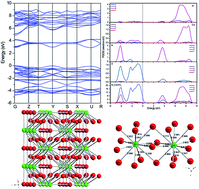
A novel Sm3+-doped Sr2CaWO6 (SCWO) red phosphor, synthesized though a solid-state reaction, was reported. Its crystal structure was analyzed and refined via the Rietveld full-pattern fitting method based on XRD patterns. The CASTEP module of Materials Studio was used to investigate the band structure and density of states of the SCWO. The optical band gap was calculated through the UV-vis diffuse reflectance spectrum and compared with the value predicted by the DFT method. Raman spectra were recorded to confirm the substitution of cations by Sm3+ ions. The broad W–O charge transfer band and narrow excitation band at 406 nm from Sm3+ ions have comparable intensities in SCWO:Sm3+. After the introduction of charge compensators Li+, Na+ or K+, the intensity of the near-UV excitation band at 406 nm was almost twice as much as before. The profiles of the emission spectra under excitation into the charge transfer absorption and f–f transition of Sm3+ are different, and low-symmetry Sm3+ centres are preferentially excited via f–f absorption transitions. The intensity ratios of electronic, magnetic dipole-allowed transitions under different radiations show that the charge compensators can influence the chemical environment around Sm3+.


Introduction

Solid-state lighting devices based on white light-emitting diodes (LEDs) are now taking off as a potential industry, and phosphor-converted LEDs are regarded as a new lighting source for the next generation.1–3 White LEDs are not just highly efficient, but are also energy-saving, compact, mercury-free and have long lifetimes.4,5 The application of LEDs is now expanding from point light sources to general illumination, demanding a high-quality white light source.6 Phosphors play a key role in producing white light with satisfactory colour rendering index (CRI) as well as high efficiency. Currently, the most common commercial white LEDs employ a blue LED coated with YAG:Ce3+ yellow phosphors, because of their simplicity and cost-saving in fabrication.7,8 However, these white LEDs have a low CRI because of their deficient emission in the red spectral region. In attempts to improve their performance, usually red phosphors have been incorporated.9–11 Another approach to white light is combining near-UV LEDs with red/green/blue tri-color phosphors.12–14 Therefore, it is urgent to search for stable and highly-efficient red phosphors to meet the requirements for white LEDs with better performance.

Recently, there has been interest in tungstate compounds as potential hosts for rare-earth-activated red phosphors, due to their good stability under various physical conditions.15–17 The general formula for tungstates with double perovskite structure is A2BWO6. The BII and W6+ ions in the three-dimensional network are ordered in such a way that every WO6 octahedron has only BIIO6 octahedra as nearest neighbors, and the A cations are located in the spaces between them.18,19 Cation site A has various coordination numbers from eight to twelve due to the tilt and rotation of BIIO6 and WO6 octahedra along their crystallographic axes.20 The luminescence properties of phosphors are closely related to the composition and local environment of the host lattice. Tungstate compounds can absorb ultraviolet (UV) light efficiently and give blue luminescence because they possess O–W charge transfer transitions.21,22 The trivalent Sm3+ (4f5) ion is a common activator which has been used in many kinds of host compounds for red phosphors.23–26 The Sm3+ ion has narrow excitation bands in the near-UV and blue region and emission bands in the reddish-orange light region, due to intrinsic 4f–4f transitions.23,25

In this paper, SCWO:2%Sm3+ and SCWO:2%Sm3+, 2%M+ (M = Li, Na and K) were synthesized by solid-state reactions. The crystal structure analysis and refinement of SCWO were carried out based on XRD patterns. Band structure and density of states calculations were performed using the CASTEP mode of Materials Studio, and the optical band gap was also estimated from the UV-vis diffuse reflection spectrum. Raman spectra were measured to confirm the sites substituted by Sm3+ ions. The photoluminescence properties, charge compensation and luminescence lifetimes of the phosphors were investigated and discussed in detail. The results indicated that SCWO:2%Sm3+, 2%M+ (M = Li, Na and K) can absorb near-UV light efficiently and give red emission, and that it is a promising red phosphor for near-UV LEDs.

Experimental

Sample preparation

The samples SCWO:2%Sm3+ and SCWO:2%Sm3+, 2%M+ (M = Li, Na and K) were prepared by a solid-state reaction technique. The starting materials were SrCO3 (Aldrich, 99.9%), CaCO3 (Junsei chemicals, 99.5%), WO3 (Aldrich, 99.995%), Sm2O3 (Aladdin, 99.5%), Li2CO3 (Aldrich, 99.997%), Na2CO3 (Aldrich, 99.995%) and K2CO3 (Yakuri Pure Chemicals Co. LTD., Tokyo, Japan, 99.60%). The raw materials were weighed in stoichiometric proportions and then mixed in an agate mortar. After 30 minutes of grinding, the uniformly mixed materials were firstly pre-fired at 850 °C for 5 h, and then the powders were reground to improve their homogeneity. After that, the precursors were calcined at 1200 °C for 12 h.

Characterization and calculation

X-ray diffraction (XRD) measurements of the as-prepared samples were carried out using a Philips X’Pert/MPD diffraction system with Cu-Kα1 irradiation (λ = 1.5406 Å), and high-resolution X-ray diffraction was recorded using a Bruker D8 Advance X-ray diffractometer over an angular (2θ) range of 10–125° with a 0.02° scanning step. UV-vis diffuse reflectance spectra (DRS) were obtained using a V-670 (JASCO) UV-vis spectrophotometer. Raman spectra were measured using a Raman/PL spectrometer (Horiba Jobin-Yvon, LabRAM HR). Photoluminescence excitation (PLE) and emission (PL) spectra were collected using a Photon Technology International (PTI) spectrofluorimeter with a 60 W Xe arc lamp, and lifetimes were measured using a phosphorimeter attached to the main system with a Xe flash lamp (25 W).

In the present band structure and density of state (DOS) calculations of SCWO, the plane wave pseudo-potential approach based on density functional theory (DFT) was used. The CASTEP program was employed to perform geometry optimization using the Broyden–Fletcher–Goldfarb–Shanno (BFGS) algorithm. The convergence thresholds in geometry optimization cycles for the energy difference, the maximal ionic Hellmann–Feynman force, the maximum stress and the maximal displacement were set as 5.0 × 10⁻⁷ eV per atom, 0.01 eV Å−1, 0.02 GPa and 5.0 × 10⁻⁴ Å, respectively. The generalized gradient approximation (GGA) by the Perdew–Burke–Ernzerhof (PBE) formulation was chosen. The cutoff energy was 480 eV, and Brillouin zone integration was represented using the K-point sampling scheme of a 5 × 6 × 6 Monkhorst–Pack grid. Ultrasoft pseudopotentials were used to approximate the core electrons.

Results and discussion

Crystal structure analysis and refinement

The phase purities of the Sm3+-doped SCWO and the as-prepared samples with Li+, Na+ and K+ as charge compensators were investigated, and their XRD patterns are given in Fig. 1. As indicated in Fig. 1, all the diffraction peaks of the samples can be indexed into the standard SCWO (JCPDS file no. 76-1983). It can be observed that the diffraction peaks of all samples shifted toward higher angles compared with the standard pattern. This can be attributed to the replacement of Sr2+ ions (CN = 12, 0.144 nm) with Sm3+ (CN = 12, 0.124 nm), Li+ (CN = 6, 0.076 nm), Na+ (CN = 12, 0.139 nm) or K+ (CN = 12, 0.164 nm) ions. The lattice parameter refinements of the samples were performed using MDI Jade 5.0 based on the given XRD patterns, and the corresponding results are shown in Table 1. The pure SCWO, which presents a double-perovskite structure, has an orthorhombic lattice with a space group of Pmm2 and lattice constants of a = 8.2033 Å, b = 5.7676 Å and c = 5.8489 Å, with Z = 2 and cell volume V = 276.73 Å3. Compared with the pure SCWO crystals, the cell parameters and volumes of the doped samples were reduced. The lattice volume shrinkage with charge compensators is not consistent, considering the ionic sizes. The reason may be that the lattice parameter refinements, based on low-resolution XRD patterns using MDI Jade 5.0, were not very accurate, and can only be used to analyze qualitatively.
image file: c5ra15572j-f1.tif
Fig. 1 The X-ray diffraction patterns of SCWO:2%Sm3+ and SCWO:2%Sm3+, 2%M+ (M = Li, Na and K).
Table 1 The refined lattice parameters of SCWO doped with Sm3+ and charge compensator Li+, Na+ or K+
Samples a (Å) b (Å) c (Å) Volume (Å3)
SCWO 8.2033 5.7676 5.8489 276.73
SCWO:2%Sm3+ 8.15687 5.74478 5.82314 272.87
SCWO:2%Sm3+, 2%Li+ 8.16213 5.7447 5.82431 273.10
SCWO:2%Sm3+, 2%Na+ 8.15721 5.73899 5.82387 272.64
SCWO:2%Sm3+, 2%K+ 8.16244 5.73817 5.81908 272.55


Structure refinement was performed for the Sm3+-doped SCWO using the Le Bail and Rietveld methods using the software General Structure Analysis System (GSAS). The initial structural models were SCWO with space group symmetry Pmm2 (25) and SrWO4 with space group I41/a (88), and the corresponding fitting patterns are shown in Fig. 2. The reliability factors of the refinement are Rwp = 12.15%, Rp = 8.53% and χ2 = 5.643. The refined cell parameters of SCWO are a = 8.1963 Å, b = 5.7680 Å and c = 5.8507 Å, with Z = 2 and cell volume V = 276.60 Å3, which are consistent with the shrinkage of the unit cell deduced from the low-resolution XRD patterns.


image file: c5ra15572j-f2.tif
Fig. 2 Experimental (black circles) and calculated (red solid line) XRD patterns and their difference (blue solid line) for the fit to the data collected for SCWO:2%Sm3+, by the GSAS program. The short magenta and green vertical lines show the positions of Bragg reflections of the calculated patterns.

Electronic structure and optical band gap

Before the band structure and density of states calculations, geometry optimization was first performed. Fig. 3(a) shows the structure of the SCWO 2 × 2 × 2 super cell, and it can be seen that both Ca2+ and W6+ ions occupy six-fold octahedral sites. Every WO6 octahedron has only six CaO6 octahedra as nearest neighbors, and Sr2+ ions are located at the 12-coordination sites between them. In double-perovskite A2BIIBVIO6, the relative arrangement of BIIO6 and BVIO6 octahedra are governed largely by the tolerance factor, image file: c5ra15572j-t1.tif, where rA and rO are the ionic radii of A and oxygen, and rB is the average ionic radius of BII and BVI.27 Herein, rA = 0.144 nm, rO = 0.140 nm and rB = (0.1 + 0.06)/2 = 0.08 nm, therefore τ = 0.913. In the ideal cubic structure for which τ = 1, the BII–O–BVI bridge is linear. Where τ < 1, it means that the radius of the A cation is relatively small, and thus the double-perovskite will reduce the size of the 12-coordination sites by cooperatively tilting the BIIO6 and BVIO6 octahedra or by bending the BII–O–BVI bridge.28 The chemical bond lengths of Sr–O, Ca–O and W–O in SCWO before and after geometry optimization are given in Table 2. Fig. 3(d) indicates that there are two kinds of Sr2+ ions in SCWO, and both of them are surrounded by twelve oxygens. Combined with the information given in Table 2, it can be found that the Sr2–O bond lengths showed significant changes, especially the Sr2–O6 bond. The original lengths of the Sr2–O6 bond were 2.8707 Å and 2.9874 Å, and they became 2.6470 Å and 3.2132 Å, respectively, after geometry optimization, which is more similar to the coordination conditions of Sr1. In addition, it is easy to find that the CaO6 and WO6 octahedra have become distorted away from regular geometries.
image file: c5ra15572j-f3.tif
Fig. 3 (a) The structure of the SCWO 2 × 2 × 2 super cell. (b) Ca–O and W–O bonding. (c) Sr–O bonding. (d) Coordination conditions of Sr1 and Sr2 in the SCWO 2 × 2 × 2 super cell.
Table 2 Comparison of chemical bond lengths (Å) of SCWO before and after geometry optimization
Chemical bond Number of bonds Bond length before optimization Bond length after optimization Chemical bond Number of bonds Bond length before optimization Bond length after optimization
Sr1–O1 2 3.1324 3.099 W1–O1 2 1.8893 1.8869
Sr1–O2 2 2.8222 2.8148 W1–O2 2 1.8893 1.9384
Sr1–O3 2 2.848 2.8829 W1–O5 2 1.8868 1.913
Sr1–O4 2 2.848 2.842 W2–O3 2 1.8893 1.8869
Sr1–O5 1 2.6435 2.6518 W2–O4 2 1.8893 1.9384
Sr1–O5 1 3.2263 3.2085 W2–O6 2 1.8868 1.913
Sr1–O6 2 2.885 2.8856 Ca1–O1 2 2.2179 2.194
Sr2–O1 2 2.7604 2.8813 Ca1–O2 2 2.2179 2.1976
Sr2–O2 2 3.0835 2.8445 Ca1–O6 2 2.2341 2.2001
Sr2–O3 2 2.8772 3.0962 Ca2–O3 2 2.2179 2.1939
Sr2–O4 2 2.9407 2.8161 Ca2–O4 2 2.2179 2.1974
Sr2–O5 2 2.9097 2.8857 Ca2–O5 2 2.2341 2.1994
Sr2–O6 1 2.8707 2.6470        
Sr2–O6 1 2.9874 3.2132        


To understand the electronic origin of the optical transitions and the chemical bonding properties, the band structure and density of states were investigated by the DFT method. The calculated band structure along the high-symmetry points of the first Brillouin zone for SCWO is shown in Fig. 4(a). It can be found that the lowest energy of the conduction bands (CBs) is located at the U point, and the highest energy of the valence band is at point G. The energy gap between the lowest conduction band point and the highest valence band point is 2.887 eV, which also indicates that SCWO is an indirect band gap insulator. Fig. 4(b) presents the total density of states (DOS) of SCWO, and the partial density of states (PDOS) is shown in Fig. 5. From Fig. 5, it can be found that the main contributor into the bottom of the conduction band of SCWO is the W 5d orbital, and that the O 2p orbital is the main contributor into the top of the valence band.


image file: c5ra15572j-f4.tif
Fig. 4 Calculated band structure (a) and total densities of states (b) of SCWO near the Fermi energy level (EF). The Fermi energy is the zero of the energy scale.

image file: c5ra15572j-f5.tif
Fig. 5 Partial densities of states of SCWO and the atoms constituting SCWO: strontium, calcium, tungsten and oxygen.

Fig. 6 gives the UV-vis diffuse reflectance spectrum of SCWO, and the inset shows the optical band gap of SCWO calculated using the Kubelka–Munk function. The SCWO host lattice shows an energy absorption ability in the UV region, and the absorption edge is near 300 nm. The strong absorption that occurred in the UV region resulted from electron excitation from the valence to the conduction band in SCWO.


image file: c5ra15572j-f6.tif
Fig. 6 Diffuse reflectance spectrum of SCWO. The inset shows the determination of the optical band gap of SCWO using the Kubelka–Munk function.

The optical band gap, Eg, can be calculated from the UV-vis DR spectrum using the following equation:29

 
αhν ∝ (Eg)n, (1)
where α is the absorbance, h is the Planck constant, ν is the photon energy, and n is determined by the transition type (n = 1/2, 2, 3/2 or 3 for allowed direct, allowed indirect, forbidden direct and forbidden indirect electronic transitions, respectively). In this case, SCWO has been confirmed to be an indirect band gap material and, therefore, n = 2:
 
(αhν)1/2Eg. (2)

From a plot of (αhν)1/2 versus hν, the band gap Eg is evaluated by extrapolating the straight line to (αhν)1/2 = 0. The value of the optical band gap Egap is determined to be 3.436 eV for the non-doped SCWO, which is larger than the calculated value by 0.549 eV. The inconsistency between the experimental band gap and the calculated one is generally accepted because DFT calculations usually underestimate the band gap energies of insulators and semiconductors.

Raman spectra

Raman spectra of SCWO:2%Sm3+, SCWO:2%Sm3+, 2%Li+, SCWO:2%Sm3+, 2%Na+ and SCWO:2%Sm3+, 2%K+ were measured to identity the cation site substitutions. The spectra in Fig. 7 display Raman shifts at about 100–200, 445 and 820 cm−1. Previous work revealed that the peaks at 100–200, 445 and 820 cm−1 can be assigned to the T2g(1), T2g(2) and A1g modes, respectively.30 According to group theory analysis of SCWO, the A1g mode is related to the stretch vibration of the oxygen ion of the WO6 and CaO6 octahedra. The T2g(1) mode is an A-site-cation-related vibration, and can be represented as the vibration between Sr and the WO6 group. In the Raman spectra in Fig. 7, the T2g(1) mode splits into four peaks, meaning that the symmetry of the Sr site is lowered. A comparison of partial Raman spectra profiles is given in Fig. 8. The four peaks at around 150 cm−1 shift to larger wavenumber upon alkali cation incorporation; however, the peak at around 820 cm−1 is almost unchanged, which implies that the Sm3+ ions are mostly incorporated into the Sr2+ site of the SCWO.
image file: c5ra15572j-f7.tif
Fig. 7 Raman spectra of SCWO:2%Sm3+ and SCWO:2%Sm3+, 2%M+ (M = Li, Na and K).

image file: c5ra15572j-f8.tif
Fig. 8 Raman spectra in the ranges of 100–200 cm−1 and 350–1000 cm−1 of (a) SCWO:2%Sm3+, (b) SCWO:2%Sm3+, 2%Li+, (c) SCWO:2%Sm3+, 2%Na+ and (d) SCWO:2%Sm3+, 2%K+.

Photoluminescence properties

Fig. 9 displays the photoluminescence excitation (PLE) spectra of the as-prepared Sm3+-doped SCWO phosphor and the samples with Li+, Na+ or K+ as charge compensators. The PLE spectra monitored at 646 nm consist of a broad band and some narrow bands; the former is referred to as the charge transfer band and the latter is from the Sm3+ ions. According to the band structure and density of states analysis above, the top of the valence band is dominated by the 2p orbital of the O atom, and the W 5d orbital is the main contributor to the bottom of the conduction band. Therefore, the broad excitation band is attributed to the charge transfer process of an oxygen 2p electron going into the empty W 5d orbital. The narrow bands, originating from the f–f transitions of Sm3+ ions, can be assigned to the electronic transitions from 6H5/2 to 6H9/2 (345 nm), 6H7/2 (354 nm), 4D3/2 (363 nm), 4P7/2 (377 nm), 4L11/2 (390 nm), 4L13/2 (406 nm), 4P5/2 (419 nm), 4G9/2 (439 nm), 4F5/2 (450 nm), 4I13/2 (462 nm), 4I11/2 (467, 471 nm), 4I11/2 (479 nm) and 4I9/2 (488 nm). It can be found that the PLE intensity of SCWO:Sm3+ is obviously enhanced after co-doping with Li+, Na+ or K+ ions. The excitation bands of Sm3+ ions in the SCWO:Sm3+, Na+ phosphor show the strongest intensity. Sm3+ ions are expected to occupy Sr2+ sites in SCWO:Sm3+, and it is difficult to maintain the charge balance. Therefore, the positive-charge defects produced, SmSr+, will negatively affect the luminescence. However, when alkali metal ions, M+, occupy Sr2+ sites, a negative-charge defect, MSr, will be obtained, which can counteract the impact of the decrease in luminescence caused by the SmSr+ defects. Of the different alkali metal ions acting as the charge transfer compensators (Li+, Na+ or K+), the radius of Na+ is most similar to that of Sr2+ ions, and therefore the most intense luminescence happens in SCWO:Sm3+ phosphors with Na+ as a charge compensator.
image file: c5ra15572j-f9.tif
Fig. 9 Excitation spectra of SCWO:2%Sm3+ and SCWO:2%Sm3+, 2%M+ (M = Li, Na and K), monitored at 646 nm.

Another interesting phenomenon observed in Fig. 9 is that the intensity of the excitation band at 406 nm almost doubled after charge compensators were introduced; however, that of the W–O charge transfer band was not enhanced significantly. In order to investigate the influence of charge compensators on intrinsic excitation of the host and f–f transitions from Sm3+, the emission spectra of SCWO:Sm3+, SCWO:Sm3+, Li+, SCWO:Sm3+, Na+ and SCWO:Sm3+, K+ exposed to 306 nm and 406 nm radiation are given in Fig. 10 and 11.


image file: c5ra15572j-f10.tif
Fig. 10 Emission spectra of SCWO:2%Sm3+ and SCWO:2%Sm3+, 2%M+ (M = Li, Na and K) excited at 306 nm.

image file: c5ra15572j-f11.tif
Fig. 11 Emission spectra of SCWO:2%Sm3+ and SCWO:2%Sm3+, 2%M+ (M = Li, Na and K) excited at 406 nm.

The emission spectra of the samples in Fig. 10 and 11 exhibited three emission bands, which are assigned to 4G5/26H5/2 (563, 567, 576 nm), 4G5/26H7/2 (600, 605, 615 nm) and 4G5/26H9/2 (646 nm) transitions. The major part of the 4G5/26H5/2 transition is magnetic-dipole-allowed, and the 4G5/26H9/2 electronic transition is purely electric dipole dominated. For the 4G5/26H7/2 transition, the magnetic dipole character is very low.31 The intensity ratio I(4G5/26H9/2)/I(4G5/26H5/2), denoted as R1, can be used to measure the departure from centrosymmetry of sites occupied by Sm3+ ions. The ratio I(4G5/26H7/2)/I(4G5/26H5/2), denoted as R2, can also be used to indicate the polarizability of the chemical environment around Sm3+. Based on the PL spectra data, R1 and R2 values were calculated and are listed in Table 3. It can be found that for SCWO:2%Sm3+, when the excitation wavelength is 406 nm, both R1 and R2 are increased significantly compared with the situation when the radiation wavelength is 306 nm. Because the 4G5/26H9/2 and 4G5/26H7/2 transitions are mainly electric-dipole-allowed ones, the bigger the R1 and R2 values of the emission, the more these are related to low-symmetry Sm3+ centres. Therefore it can be concluded that low-symmetry Sm3+ centres tend to be excited via f–f transitions.32 Both R1 and R2 in SCWO:2%Sm3+, 2%M+ (M = Li, Na and K) increased obviously compared with the values for the SCWO:2%Sm3+ sample, when the samples were exposed to 306 nm light. In contrast, when the excitation light was 406 nm, R1 and R2 values were smaller in samples with charge compensators, although they were still larger than those obtained upon excitation by 306 nm light. That is to say, after the charge compensators were added, energy from the W–O charge transfer band preferred to transfer to Sm3+ luminescence centres with low symmetry.

Table 3 Intensity ratios R1 and R2 of SCWO doped with Sm3+ and charge compensator Li+, Na+ or K+a
λex = 306 nm R1 R2 λex = 406 nm R1 R2
a R1 = I(4G5/26H9/2)/I(4G5/26H5/2), R2 = I(4G5/26H7/2)/I(4G5/26H5/2).
SCWO:2%Sm3+ 3.097 2.132 SCWO:2%Sm3+ 3.774 2.314
SCWO:2%Sm3+, 2%Li+ 3.404 2.176 SCWO:2%Sm3+, 2%Li+ 3.620 2.248
SCWO:2%Sm3+, 2%Na+ 3.409 2.170 SCWO:2%Sm3+, 2%Na+ 3.568 2.252
SCWO:2%Sm3+, 2%K+ 3.290 2.146 SCWO:2%Sm3+, 2%K+ 3.579 2.233


Excited state dynamics of the 4G5/2 level of Sm3+

Under excitation into the 6H5/24L13/2 transition of Sm3+ (λex = 406 nm), the excited state dynamics of the 4G5/2 level of Sm3+ were measured, ending on the 6HJ levels, for the SCWO:2%Sm3+ and SCWO:2%Sm3+, 2%M+ (M = Li, Na and K) phosphors. The luminescence decay curves are depicted in Fig. 12; they can be well fitted with a first-order exponential decay model using eqn (3):
 
I(t) = I0 + A[thin space (1/6-em)]exp(−t/τ), (3)
where I and I0 are the emission intensities at time t and 0, A is a constant, t is time and τ is the decay time for an exponential component. On the basis of eqn (3) and the decay curves, lifetimes for SCWO:2%Sm3+ were determined to be 550.92, 550.81 and 531.44 μs for 563, 600 and 646 nm emissions, respectively (Fig. 12(a)). The interaction of the SCWO:Sm3+ phosphor with the excitation wavelength of 406 nm leads to the transition of Sm3+ ions from the ground level 6H5/2 to the higher 4L13/2 level. After that, Sm3+ ions usually make non-radiative transitions to the 4G5/2 state through multiple channels of cross-relaxation processes, which are due to energy transfer from the excited 4G5/2 state to the ground 6H5/2 state via the 6F11/2, 6F9/2, 6F7/2, and 6F5/2 levels, such as (4G5/2, 6F11/2) → (6H5/2, 6F5/2). Therefore, possible cross-relaxation channels can influence the lifetime of the excited 4G5/2 state. The decay curves for the SCWO:2%Sm3+, 2%M+ (M = Li, Na and K) phosphors are also given in Fig. 12, and the lifetimes corresponding to the 4G5/2 state of Sm3+ in SCWO:2%Sm3+, 2%Li+, SCWO:2%Sm3+, 2%Na+ and SCWO:2%Sm3+, 2%K+ are 716.49, 421.71 and 434.59 μs. Compared with SCWO:2%Sm3+, SCWO:2%Sm3+, 2%Na+ and SCWO:2%Sm3+, 2%K+, the longest lifetime value was observed in SCWO:2%Sm3+, 2%Li+. In SCWO:2%Sm3+, 2%Li+, due to the radius of Li+ being the smallest, the average Sr–Sr distance is the shortest and, therefore, the compensator LiSr can compensate SmSr+ more effectively than can NaSr and KSr.

image file: c5ra15572j-f12.tif
Fig. 12 PL decay curves of SCWO:2%Sm3+ (a), SCWO:2%Sm3+, 2%Li+ (b), SCWO:2%Sm3+, 2%Na+ (c) and SCWO:2%Sm3+, 2%K+ (d) under 406 nm radiation.

CIE chromaticity coordinates and quantum efficiency

The CIE chromaticity diagram for the SCWO:2%Sm3+ and SCWO:2%Sm3+, 2%M+ (M = Li, Na and K) samples is displayed in Fig. 13. As indicated in Fig. 13, the CIE coordinates for SCWO:2%Sm3+, SCWO:2%Sm3+, 2%Li+, SCWO:2%Sm3+, 2%Na+ and SCWO:2%Sm3+, 2%K+ are (0.5952, 0.4022), (0.6001, 0.3984), (0.5998, 0.3987) and (0.5992, 0.3993), respectively, which are close to those of commercial red Sr2Si5N8:Eu2+ phosphors (0.62, 0.37). The quantum efficiency of the Sr2CaWO6:2%Sm3+, 2%Na+ was measured, because the emission intensity of Sr2CaWO6:2%Sm3+, 2%Na+ under 406 nm excitation was the most intense. Its external quantum efficiency is 5.017% and internal quantum efficiency is 21.066%. The quantum efficiency of our sample is lower compared with those of the state-of-the-art red phosphors, such as Y2O3:Eu3+. This is partly because the method that we used to synthesize the phosphors is high-temperature solid-state reaction, which usually leads to particle agglomeration and non-uniform size distribution. It is believed that the quantum efficiency can be further enhanced by controlling the particle size and morphology through optimizing the synthetic route.
image file: c5ra15572j-f13.tif
Fig. 13 CIE chromaticity coordinates of (a) SCWO:2%Sm3+, (b) SCWO:2%Sm3+, 2%Li+, (c) SCWO:2%Sm3+, 2%Na+ and (d) SCWO:2%Sm3+, 2%K+.

Conclusions

In conclusion, SCWO:2%Sm3+ and SCWO:2%Sm3+, 2%M+ (M = Li, Na and K) phosphors were prepared via a solid-state reaction method. XRD patterns show that all the samples can be indexed to orthorhombic SCWO, according to the JCPDS file no. 76-1983. The results of crystal structure refinement by GSAS program confirmed the reduced lattice parameters of SCWO unit cell after incorporation of Sm3+. More reasonable chemical bond lengths were given after geometry optimization using the program Materials Studio. The calculation results from the CASTEP mode show that the main contributor into the bottom of the conduction band of SCWO is the W 5d orbital, and that the O 2p orbital is the main contributor into the top of the valence band. The band gap is calculated to be 2.887 eV, which is smaller than the optical band gap Egap for the non-doped SCWO determined from UV-vis diffuse reflectance spectroscopy. The inconsistency between the calculated band gap and the experimental one is generally accepted because DFT calculations usually underestimate the band gaps of insulators and semiconductors. Sr2+ 12-coordination sites are confirmed to be substituted by Sm3+ ions through Raman spectra. Charge compensators can influence the local chemical environment of Sm3+, and near-UV excitation at about 406 nm is more intense than the charge transfer band in SCWO:2%Sm3+, 2%M+ (M = Li, Na and K). The emission color of SCWO:2%Sm3+, 2%Li+ (0.6001, 0.3984) is closest to that of the commercial red phosphor Sr2Si5N8:Eu2+ (0.62, 0.37).

Acknowledgements

This research was supported by the Basic Science Research Program through the National Research Foundation of Korea (NRF) funded by the Ministry of Science, ICT and Future Planning (No. 2013012655). This work also supported by the Global Frontier R&D Program (2013-073298) on Center for Hybrid Interface Materials (HIM) funded by the Ministry of Science, ICT & Future Planning. The Sm3+-doped SCWO with Li+, Na+ or K+ was supplied by the Display and Lighting Phosphor Bank at Pukyong National University.

References

  1. M. H. Crawford, LEDs for Solid-State Lighting: Performance Challenges and Recent Advances, IEEE J. Sel. Top. Quantum Electron., 2009, 15, 1028–1040 CrossRef CAS.
  2. J. Y. Tsao, Solid-state lighting: lamps, chips, and materials for tomorrow, IEEE Circuits and Devices Magazine, 2004, 20, 28–37 CrossRef.
  3. S. Ye, F. Xiao, Y. X. Pan, Y. Y. Ma and Q. Y. Zhang, Phosphors in phosphor-converted white light-emitting diodes: recent advances in materials, techniques and properties, Mater. Sci. Eng., R, 2010, 71, 1–34 CrossRef.
  4. J. Dwivedi, P. Kumar, A. Kumar, Sudama, V. N. Singh, B. P. Singh, S. K. Dhawan, V. Shanker and B. K. Gupta, Commercial approach towards fabrication of bulk and nano phosphors converted highly-efficient white LEDs, RSC Adv., 2014, 4, 54936–54947 RSC.
  5. H. Qian, J. Zhang and L. Yin, Crystal structure and optical properties of white light-emitting Y2WO6:Sm3+ phosphor with excellent color rendering, RSC Adv., 2013, 3, 9029–9034 RSC.
  6. D. G. Pelka and K. Patel, An overview of LED applications for general illumination, Proc. SPIE, 2003, 5186, 15–26 CrossRef.
  7. H. Yang, G. Zhu, L. Yuan, C. Zhang, F. Li, H. Xu, A. Yu and B. Dunn, Characterization and Luminescence Properties of YAG:Ce3+ Phosphors by Molten Salt Synthesis, J. Am. Ceram. Soc., 2012, 95, 49–51 CrossRef CAS.
  8. R. Zhang, H. Lin, Y. Yu, D. Chen, J. Xu and Y. Wang, A new-generation color converter for high-power white LED: transparent Ce3+:YAG phosphor-in-glass, Laser Photonics Rev., 2014, 8, 158–164 CrossRef CAS.
  9. X. Yan, W. Li, X. Wang and K. Sun, Facile Synthesis of Ce3+, Eu3+ Co-Doped YAG Nanophosphor for White Light-Emitting Diodes, J. Electrochem. Soc., 2012, 159, H195–H200 CrossRef CAS.
  10. Y. Pan, M. Wu and Q. Su, Tailored photoluminescence of YAG:Ce phosphor through various methods, J. Phys. Chem. Solids, 2004, 65, 845–850 CrossRef CAS.
  11. H. S. Jang, W. B. Im, D. C. Lee, D. Y. Jeon and S. S. Kim, Enhancement of red spectral emission intensity of Y3Al5O12:Ce3+ phosphor via Pr co-doping and Tb substitution for the application to white LEDs, J. Lumin., 2007, 126, 371–377 CrossRef CAS.
  12. Z. G. Xia and R. S. Liu, Tunable Blue-Green Color Emission and Energy Transfer of Ca2Al3O6F:Ce3+,Tb3+ Phosphors for Near-UV White LEDs, J. Phys. Chem. C, 2012, 116, 15604–15609 CrossRef CAS.
  13. C. H. Huang, P. J. Wu, J. F. Lee and T. M. Chen, (Ca,Mg,Sr)9Y(PO4)7:Eu2+,Mn2+: Phosphors for white-light near-UV LEDs through crystal field tuning and energy transfer, J. Mater. Chem., 2011, 21, 10489–10495 RSC.
  14. C. Guo, H. Jing and T. Li, Green-emitting phosphor Na2Gd2B2O7:Ce3+, Tb3+ for near-UV LEDs, RSC Adv., 2012, 2, 2119–2122 RSC.
  15. B. P. Singh, M. Maheshwary, P. V. Ramakrishna, S. Singh, V. K. Sonu, S. Singh, P. Singh, A. Bahadur, R. A. Singh and S. B. Rai, Improved photo-luminescence behaviour of Eu3+ activated CaMoO4 nanoparticles via Zn2+ incorporation, RSC Adv., 2015, 5, 55977–55985 RSC.
  16. A. M. Kaczmarek, K. Van Hecke and R. Van Deun, Enhanced luminescence in Ln3+-doped Y2WO6 (Sm, Eu, Dy) 3D microstructures through Gd3+ codoping, Inorg. Chem., 2014, 53, 9498–9508 CrossRef CAS PubMed.
  17. K. V. Dabre, K. Park and S. J. Dhoble, Synthesis and photoluminescence properties of microcrystalline Sr2ZnWO6:RE3+ (RE = Eu, Dy, Sm and Pr) phosphors, J. Alloys Compd., 2014, 617, 129–134 CrossRef CAS.
  18. J. H. G. Bode and A. B. V. Oosterhout, Defect luminescence of ordered perovskites A2BWO6, J. Lumin., 1975, 10, 237–242 CrossRef CAS.
  19. G. King, S. Thimmaiah, A. Dwivedi and P. M. Woodward, Synthesis and Characterization of New AA’BWO6 Perovskites Exhibiting Simultaneous Ordering of A-Site and B-Site Cations, Chem. Mater., 2007, 19, 6451–6458 CrossRef CAS.
  20. P. M. Woodward, Octahedral tilting in perovskites. II. structure stabilizing forces, Acta Crystallogr., Sect. B: Struct. Sci., 1997, 53, 44–66 CrossRef.
  21. S. Basu, B. Sanyasi Naidu, B. Viswanadh, V. Sudarsan, S. N. Jha, D. Bhattacharyya and R. K. Vatsa, Nature of WO4 tetrahedra in blue light emitting CaWO4 probed through the EXAFS technique, RSC Adv., 2014, 4, 15606–15612 RSC.
  22. X. Dong, Z. Fu, Q. Wang, G. Sun and Z. Dai, Synthesis and investigation of luminescence properties of Eu3+-doped cubic perovskite Ba3Y2WO9, Opt. Mater., 2013, 35, 1577–1581 CrossRef CAS.
  23. G. Zhu, Z. Ci, Y. Shi and Y. Wang, Synthesis and photoluminescence properties of Ca19Mg2(PO4)14:Sm3+ red phosphor for white light emitting diodes, Mater. Res. Bull., 2014, 55, 146–149 CrossRef CAS.
  24. J. Wu, S. Shi, X. Wang, J. Li, R. Zong and W. Chen, Controlled synthesis and optimum luminescence of Sm3+-activated nano/submicroscale ceria particles by a facile approach, J. Mater. Chem. C, 2014, 2, 2786–2792 RSC.
  25. M. S. Kim and J. S. Yu, Synthesis and luminescent properties of nanocrystalline CaYAlO4:Sm3+ phosphors, Phys. Status Solidi B, 2013, 250, 374–377 CrossRef CAS.
  26. P. Du, L. Song, J. Xiong, H. Cao, Z. Xi, S. Guo, N. Wang and J. Chen, Electrospinning fabrication and luminescent properties of SrMoO4:Sm3+ nanofibers, J. Alloys Compd., 2012, 540, 179–183 CrossRef CAS.
  27. G. Popov, M. Greenblatt and M. Croft, Large effects of A-site average cation size on the properties of the double perovskites Ba2−xSrxMnReO6: A d5–d1 system, Phys. Rev. B: Condens. Matter Mater. Phys., 2003, 67, 024406 CrossRef.
  28. M. H. Whangbo and H. J. Koo, Effect of Metal–Oxygen Covalent Bonding on the Competition between Jahn–Teller Distortion and Charge Disproportionation in the Perovskites of High-Spin d4 Metal Ions LaMnO3 and CaFeO3, Inorg. Chem., 2002, 41, 1920–1929 CrossRef CAS PubMed.
  29. D. L. Wood and J. Tauc, Weak Absorption Tails in Amorphous Semiconductors, Phys. Rev. B: Condens. Matter Mater. Phys., 1972, 5, 3144–3151 CrossRef.
  30. G. Blasse and A. F. Corsmit, Electronic and Vibrational Spectra of Ordered Perovskites, J. Solid State Chem., 1973, 6, 513–518 CrossRef CAS.
  31. C. K. Jayasankar and E. Rukmini, Optical properties of Sm3+ ions in zinc and alkali zinc borosulphate glasses, Opt. Mater., 1997, 8, 193–205 CrossRef CAS.
  32. C. Tiseanu, B. Cojocaru, D. Avram, V. I. Parvulescu, A. V. Vela-Gonzalez and M. Sanchez-Dominguez, Isolated centres versus defect associates in Sm3+-doped CeO2: a spectroscopic investigation, J. Phys. D: Appl. Phys., 2013, 46, 275302 CrossRef.

This journal is © The Royal Society of Chemistry 2015
Click here to see how this site uses Cookies. View our privacy policy here.