
Role of Zn-interstitial defect states on d0 ferromagnetism of mechanically milled ZnO nanoparticles

Srabantika Ghosea, Tamita Rakshitb, R. Ranganathanc and D. Jana*a
aDepartment of Physics, University of Calcutta, 92, A. P. C. Road, Kolkata 700009, India. E-mail: djphy@caluniv.ac.in; Tel: +91 33 2350 8386 ext. 442
bDepartment of Physics, Indian Institute of Technology, Kharagpur 721302, India
cCondensed Matter Physics Division (Experiment), Saha Institute of Nuclear Physics, 1/AF, Bidhannagar, Kolkata 700064, India

Received 14th July 2015 , Accepted 30th October 2015

First published on 30th October 2015


Abstract

Ferromagnetism in the nanostructures of undoped oxide semiconductors has become an exciting problem nowadays for its potential future applications in spintronics. In order to elucidate the room temperature d0 ferromagnetism of oxide semiconductors, we have investigated the changes in magnetic property of ZnO nanoparticles with the reduction of size by mechanical milling. We have observed that ferromagnetic ordering appears in the sample when the particle size decreases from 39 ± 1 nm to 30 ± 1 nm. This observation strongly supports the idea of the effect of specific grain boundaries in nanoparticles. The results of Raman scattering also support this observation. From photoluminescence spectra shifted green emissions have been found for ferromagnetic samples. This indicates clearly two different origins for green emissions that are strongly related to the changes in magnetic property. Observations from electron spin resonance spectra suggest that zinc related interstitial defects are significant to give rise to this ferromagnetic coupling. An impurity level formed by the interstitial defects at the surfaces could satisfy the Stoner criteria for the occurrence of band ferromagnetism for these samples.

Introduction

After the prediction of room temperature (RT) ferromagnetism (FM) in transition metal doped wide band gap semiconductors by T. Dietl et al.1 intense research has been carried out on dilute magnetic semiconductors (DMSs) in the last fifteen years. Among all oxide semiconductor ZnO based DMSs have received considerable attention due to their potential applications in spintronics. There are also some reports where the observed moment exceeds the maximum possible spin moment per dopant cation or the dopant atoms are found to be paramagnetic where the sample as a whole is showing FM.2,3 Interestingly studies have found FM even in undoped ZnO4–6 and other undoped semiconducting oxides7–9 prepared using different synthesis techniques and it is termed as d0 FM.10

The attractive properties of ZnO such as wide band gap and large excitonic binding energy (∼3.37 eV and 60 meV respectively at RT), piezoelectricity, large electronegativity of O atom leading to strong p–d exchange between localized spins and carriers for DMSs;11 make it the most studied oxide semiconductor in the last decade. However, the main obstacle to use this material for the fabrication of potential devices is the lack of understanding on the role of defects which largely affect its all properties. In case of d0 FM of ZnO, reports supporting intrinsic defects such as zinc vacancies (VZn),12,13 oxygen vacancies (VO),14,15 zinc interstitials (IZn)16,17 as well as oxygen interstitials (IO)18 to be the origin of FM have been published. However, even after considerable research in ZnO the correct mechanism of d0 FM is still not understood. All of these reports are based on the studies of ZnO nanoparticles synthesized by such techniques which do not allow us to observe the gradual change of magnetic property from diamagnetic to ferromagnetic. As the FM is observed in the samples with lower size/dimension therefore it has been identified that this FM is closely related to the defects at the surface regions.19,20 Ball milling is the technique which gives us the opportunity to study this magnetic modification gradually. However there exists very few attempts to study the FM of mechanically milled undoped ZnO nanoparticles so far.20,21 In this present work the size of ZnO nanoparticles have been reduced in several steps using a planetary ball-milling grinder for different milling time (tm). Magnetic property is modified from diamagnetic to ferromagnetic due to this reduction of size. High saturation magnetization (Ms) of 0.0015 emu g−1 has been observed for 960 minutes (16 hours) of milling. We have restricted tm in lower value to focus our study on the magnetic transition region.

Experimental

As-supplied ZnO material (ZnO-0) with 99.99% purity (Sigma-Aldrich) was ball milled in an agate container with agate ball for different tm (60, 240, 480 and 960 minutes) in pure N2 atmosphere. To avoid the effect (if any) of the O2 gas on the surface defect states of ball milled nanoparticles, we have chosen N2 gas as the milling environment. A report on FM of ZnO nanoparticles prepared by ball-milling in ambient condition has been reported earlier.20 The ball to mass ratio was taken as 5[thin space (1/6-em)]:[thin space (1/6-em)]1. To avoid air contamination, unexpected impurity and also to reduce the heat dissipation generated during milling time, the whole milling process had been carried out taking intervals of 15 minutes after every 30 minutes of milling. Samples are named as ZnO-0, ZnO-60, ZnO-240, ZnO-480 and ZnO-960 according to the variation of tm. X-ray diffraction (XRD) patterns of all samples were recorded in a TTRAX III rigaku X-ray diffractometer in Bragg–Brentano geometry using Cu Kα (1.542 Å) radiation. The microstructural analysis was performed by mounting the sample on a carbon coated Cu grid with the help of transmission electron microscope (TEM) (JEOL, Model JEM-2010). The magnetic measurements are carried out using a super-conducting quantum interference device (SQUID) magnetometer (Quantum Design MPMS SQUID VSM EVERCOOL: SVSM7). Raman scattering (RS) spectra were taken by a confocal Raman imaging system (WITec GmBH; alpha300RS). The UHTS 300 spectrograph is equipped with a Peltier cooled back-illuminated CCD camera with better than 90% QE in visible excitation. All RS spectra were collected by using 532 nm line of laser source at RT in air. Photoluminescence (PL) measurements at RT were carried out with He–Cd laser operating at 325 nm as an excitation source with an output power of 45 mW and a cooled Hamamatsu R928 photomultiplier detector. Finally, electron paramagnetic resonance (EPR) measurements are performed on a (JEOL FA200) spectrometer operating at an X-band frequency (9.4 GHz).

Results and discussions

The XRD patterns recorded at RT for all the prepared samples are shown in Fig. 1. XRD patterns confirm that all samples have single phase wurtzite structure (P63mc). Crystallite size of the sample reduces from 49 nm (ZnO-0) to 24 nm (ZnO-960) due to the effect of 960 minutes of mechanical milling. TEM images confirm that the average grain size decreases to 23 nm for ZnO-960 (Fig. 2). As there is some agglomeration present in TEM images well separated particles (as indicated by arrows in Fig. 2) have been considered from several images. TEM results are in good agreement with the XRD results. To avoid any confusion for the following discussion the particle size will be referred to the results of XRD. Inset of Fig. 2 shows the HRTEM image of ZnO-960. The lattice spacing is 2.64 nm corresponds to (002) plane. Lattice parameters of all samples are calculated by Rietveld refinement method (Fullprof program) using pseudo-voigt function. The obtained refinements of ZnO-0 and ZnO-960 are shown in Fig. 3. The R-factors are below 3% for all refinements. Comparing Rietveld refinement results probability of incorporation of any significant impurity in the sample due to ball milling process has been ruled out completely. Lattice parameters a and c of all samples obtained from Rietveld refinement are shown in Fig. 4(a) and (b). An increment in the values of both lattice parameters with increasing milling time has been observed. Similar enhancement in the values of lattice parameters for milling time upto 50 hours is also reported.21,22 This effect is due to the increase in defect density in the grounded medium. Defects introduce strain in the material and thus the values of lattice parameters can change.23 As the sample size reduces there is an increase in the surface to volume ratio which is proportional to 1/D where D is the average particle size of the sample. Surfaces of nanoparticles act as a sink for the defect states. The crystallite size of ZnO nanoparticles decreases with increasing tm as shown in Fig. 4(c). The mechanical milling process incorporates different types of surface defects in the grounded material. However, from earlier observations, it has been found that due to mechanical milling VZn are more likely to be incorporated in the material than other type defects.22,23
image file: c5ra13846a-f1.tif
Fig. 1 X-ray diffraction patterns of all samples at room temperature. All samples have pure wurtzite structure (P63mc).

image file: c5ra13846a-f2.tif
Fig. 2 TEM image of ZnO-960. Some well separated particles are indicated by arrows. Inset shows HRTEM image of this sample.

image file: c5ra13846a-f3.tif
Fig. 3 Results of Rietveld refinement for as-supplied ZnO (ZnO-0) and highest milled ZnO (ZnO-960) samples.

image file: c5ra13846a-f4.tif
Fig. 4 Variation of lattice parameter a [(a)], lattice parameter c [(b)] and crystallite size [(c)] of the samples with milling time.

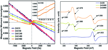
The magnetization vs. field (MH) results obtained from SQUID measurements at RT of all samples are shown in Fig. 5. It has been observed that ZnO-0 and ZnO-60 are diamagnetic samples. For ZnO-240 however, very small ferromagnetic moment is generated. This moment increases for ZnO-480 and ZnO-960 samples gradually. Highest value of saturation magnetization (Ms = 0.0015 emu g−1) is observed for ZnO-960. Small but sizeable coercivity (Hr ∼ 50 Oe) and remanence (Mr ∼ 6 × 10⁻⁵ emu g−1) are present in ZnO-960 at RT (inset of Fig. 5). The order of magnitude of Ms is in good agreement with the recently published reports of FM for ball milled undoped semiconducting oxides.7,20 Values of Ms and Hr of three ferromagnetic samples are listed in Table 1. Fig. 6 depicts the MH curves of three ferromagnetic samples after subtracting the diamagnetic background. Inset of this figure shows the magnetization vs. temperature (MT) curves for ZnO-960 sample. A distinct bifurcation between field cool (FC) and zero field cool (ZFC) MT curves is in agreement with earlier reports on undoped ZnO systems.22,24 For FC MT curve the applied field is 1 kOe. MT result confirms that Curie temperature (TC) of ZnO-960 is above RT. It is interesting to note that ferromagnetic hysteresis in the MH curve originates when the particle size of the sample decreases from 39 nm to 30 nm for ZnO-60 and ZnO-240 respectively. Therefore in between these two sizes there exists a critical value of particle size where the modification of magnetic property of ZnO nanoparticles occurs. If we consider the specific grain surface area (SGB)19 as 1.65/D then values of SGB increases from 4.3 × 10⁷ m−1 to 5.5 × 10⁷ m−1 for ZnO-60 and ZnO-240 respectively. Hence the empirical threshold value of SGB for the occurrence of FM in ZnO nanoparticles lies in between these two values. Straumal et al.19 have predicted this threshold value of SGB is located in the vicinity of 5 × 10⁷ m−1 which is in good agreement with our observation. From the research works carried out for last ten years, it has been understood that enhancement in surface area and dangling bonds and/or an increase in the defects presented at the surfaces of the sample could be the reason behind this modification in magnetic property from diamagnetic to ferromagnetic one.19,20


image file: c5ra13846a-f5.tif
Fig. 5 MH curves of all sample at room temperature. The inset shows the magnified low field region of MH curve for ZnO-960 sample.
Table 1 Values of saturation magnetization (Ms) and coercivity (Hr) of three ferromagnetic samples
Sample name Ms (emu g−1) (±0.0001) Hr (Oe) (±5)
ZnO-240 0.0005 10
ZnO-480 0.0009 22
ZnO-960 0.0015 50


image file: c5ra13846a-f6.tif
Fig. 6 MH curves of three ferromagnetic samples after subtracting the diamagnetic background. The inset shows the MT (FC and ZFC) curves for ZnO-960 sample.

Before discussing the interplay of the surfaces and the defects it is interesting to note that the wurtzite structure has a hexagonal unit cell with two lattice parameters a (basal plane parameter) and c (axial parameter) in the ratio c/a = 1.633 for an ideal structure. In real ZnO crystal experiments show that c/a ratio is lower than this ideal value. The internal parameter u is defined as the anion–cation bond length divided by c along the c-axis. Therefore the nearest neighbour distance (b) along c-axis can be expressed as c × u. There is a strong correlation existing between c/a and u parameters. The value of c/a changes inversely with u in such a way that the distances between four tetrahedral remain unchanged. Generally, a distortion of tetrahedral angles takes place due to long range polar interactions.25 Fig. 7 shows the variation of c/a ratio obtained from the Rietveld refinement with particle size. This plot is divided into two regions ferromagnetic and diamagnetic as observed from SQUID measurements. In the diamagnetic region, reduction of particle size increases the c/a ratio but this ratio decreases with the lowering of particle size when the sample becomes ferromagnetic. The individual value of a and c increases for all samples with the reduction of size (a ≈ 3.2498 Å and c ≈ 5.2067 Å for ZnO-0 and a ≈ 3.2511 Å and c ≈ 5.2086 Å for ZnO-960). This is due to the appearance of internal strain in the sample. Strain in the nanoparticles increases due to the incorporation of large number of defects by the ball-milling process. From Fig. 7 it can be understood that in ferromagnetic regime this extensive strain is less active in the polar planes (i.e. at zinc terminated (0001) and oxygen terminated (000[1 with combining macron]) surfaces). Therefore it can be suggested that below 30 nm structure of ZnO nanoparticles is modified significantly due to the appearance ferromagnetic interactions.


image file: c5ra13846a-f7.tif
Fig. 7 Variation of c/a ratio with particle size as estimated from Rietveld refinement.

RS spectra give important informations about the microscopic nature of structure and morphological disorder which are strongly correlated with the optical phonons in nanomaterials. Being polar semiconductor additional Raman modes other than optical and acoustical phonons may appear for ZnO depending on its dimension/size (L), excitation wavelength (λ) and the Bohr exciton radius (rB). For nanostructures rBLλ (10 nm < L < 100 nm) surface phonon modes appear in RS spectra due to the presence of large surface area. Fig. 8 depicts RS spectra of all ZnO samples at RT. For wurtzite ZnO the irreducible representation at Γ point is Γopt = A1 + E1 + 2E2 + 2B1, where both polar modes A1 and E1 and non-polar mode E2 are Raman active. E2 mode consists of Ehigh2 and Elow2 as indicated in Fig. 8. Ehigh2 and Elow2 are assigned to the vibrations of oxygen atoms and zinc sublattice in ZnO respectively.26,27 Ehigh2 mode also represents the band characteristics of ZnO. Both polar modes A1 and E1 get splitted into TO and LO phonons. A1(LO) and E1(LO) have very close wavenumbers and specially E1(LO) mode is very sensitive to the presence of lattice defects. Due to mechanical activation, these modes get broadened and become difficult to distinguish. Some additional broad modes appear below 200 cm−1. They are assigned to the appearance of surface defects in the sample.28 For better understanding we have deconvoluted RS spectra by least square optimized method using Lorentzian peaks as shown in Fig. 9 (ZnO-60 is similar to ZnO-0). All observed peaks in the samples can be assigned to Raman active modes of ZnO crystal and they are listed in Table 2 together with the result of the literature.29 The ratio between the intensities of E1(LO) (I1) to Ehigh2 (I2) after deconvolution is calculated and this ratio increases gradually from 0.236 (ZnO-0) to 1.478 (ZnO-480) but it reduces to 0.959 for ZnO-960. As the E1(LO) mode is related to oxygen vacancies30 therefore reduction of I1/I2 ensures a reduction in concentration of oxygen related vacancies for ZnO-960 sample. Hence the RT FM could not be related to the oxygen related vacancies. Using two dimensional Maxwell-Garnett approximation and considering plasmon contribution Šćepanović et al.28 have predicted two SOP modes at wavenumbers lower than A1(LO) mode for nanocrystalline ZnO. We have observed two SOP modes (SOP1 and SOP2) for ZnO nanocrystals as listed in Table 2 and the SOP2 mode increases drastically due to mechanical activation. This indicates a significant modification of surface area due to the appearance of defects there.28,31 As there is a reduction of correlation length at the surfaces due to the introduction of intrinsic defects the phonon confinement effect could be a dominant factor.


image file: c5ra13846a-f8.tif
Fig. 8 Raman spectra of all samples at room temperature.

image file: c5ra13846a-f9.tif
Fig. 9 Deconvoluted Raman spectra using Lorentzian peaks.
Table 2 Raman peak positions and (FWHM) in cm−1
Process ZnO-0 ZnO-240 ZnO-480 ZnO-960 Ref. 29
Ehigh2–Elow2 333 (42) 330 (38) 330 (23) 329 (29) 333
A1(TO) 386 (29) 386 (43) 386 (32) 389 (48) 378
E1(TO) 420 (31) 425 (23) 425 (24) 425 (31) 410
Ehigh2 439 (9) 438 (10) 438 (11) 438 (13) 438
2LA 481 (14) 481 (6) 481 (7) 480 (27) 483
SOP1 510 (29) 506 (8) 505 (11) 505 (9)
2Blow1; 2LA 538 (29) 526 (5) 536 (30) 538 (36) 536
SOP2 554 (18) 552 (46) 552 (36) 552 (32)
A1(LO) 569 (17) 570 (10) 570 (7) 572 (23) 574
E1(LO) 582 (30) 580 (24) 578 (25) 582 (18) 590


To understand more about the defects in ZnO nanoparticles we have studied the samples using PL spectroscopic measurement at RT. In ZnO nanostructures two different emissions broadly take place. One is the ultraviolet near band edge emission (NBE) at 382 nm due to the band to band transition including bound excitons and shallow states. This emission is considered as the characteristic emission of ZnO.32,33 The other one is the defect related broad emission (DBE) in the visible range. The ratio between NBE and DBE has been considered as the signal for the crystalline quality but this idea could be misleading as we will discuss below. The origin of DBE is however controversial and several kind of defects such as VZn, VO, IZn, IO etc. have been claimed as being responsible for DBE. It is noteworthy that in these defect states VO and IZn are donor defects whereas VZn and IO are known to be acceptor defects. These all defects however can exist in different charged states. Emissions from these defect states generally occur near blue (∼410–480 nm; Fit 2), blue-green (∼480–560 nm; Fit 3), yellow (∼560–610 nm: Fit 4) and orange-red (∼610–750 nm; Fit 5) color band. The blue luminescence is generally attributed to IZn (ref. 34) and the orange-red emission originates from IO (ref. 35) which stabilize for higher oxygen partial pressure at the surfaces. The yellow emission is attributed to doubly charged oxygen vacancies (image file: c5ra13846a-t1.tif).36 Polarized luminescence measurement indicates that green emission originates from the surfaces.37 However VZn, image file: c5ra13846a-t2.tif or surface modifications are being considered as the origin for it.38–40 This green emission has been related with the FM of undoped ZnO nanoparticles by many researchers.41 In case of our samples RT PL spectra are recorded as depicted in Fig. 10. The as-supplied ZnO-0 has two broad peaks as commonly found in bulk ZnO. The NBE is around 382 nm while DBE appears at ∼560 nm. Due to the effect of mechanical milling NBE quenches and almost disappears for the samples with tm ≥ 240 min. DBE is modified significantly due to the effect of size degradation. It is very interesting to note that DBE quenches initially with the reduction of size and reaches to the minimum for the ZnO-240; sample for which the FM has started to appear. Further reduction of size enhances DBE spectra with a significant red shift (≈30 nm) of the peak value. The intensity of DBE reaches maximum for ZnO-960. It has been already pointed out that DBE can be considered as a superposition of four color band spectra. Therefore the overall PL spectra including NBE have been fitted by five peaks (Gaussian) method. The three Gaussian peak fitting has already been employed for DBE analysis.41 Therefore the five Gaussian peak fitting of NBE and DBE as shown in Fig. 11 is also validated. Note that ratio of NBE to DBE has been increased for ZnO-60 than ZnO-0. In mechanical milling process crystalline quality always degrades with tm. Therefore it is clear that the ratio of NBE to DBE cannot be considered to verify the crystalline quality of the sample. This observation also has been found in cathodoluminescence study.38 This ratio not only depends on the presence of defect energy states in the samples but also on the transition probability between different energy levels. Interestingly it has been observed that this transition probability has dependence on the excitation energy also.34 To get the correct conclusion about the defect density of the system spectroscopic measurement other than PL such as Raman or infra-red study must be carried out.


image file: c5ra13846a-f10.tif
Fig. 10 Photoluminescence spectra of all samples at room temperature.

image file: c5ra13846a-f11.tif
Fig. 11 Deconvoluted photoluminescence spectra using Gaussian peaks.

The green and yellow bands (Fit 3 and 4) have a considerable shift for ferromagnetic ZnO-480 and ZnO-960 samples than the diamagnetic ZnO-0 and ZnO-60. Now ball-milling process favors the formation of cationic vacancies9,23 and our observations from Raman data support this. Hence the green emission (Fit 3) of these samples is attributed to the appearance of VZn. The supplied ZnO materials are generally synthesized by chemical route and oxygen vacancies are the most probable defects for those materials. Therefore, presence image file: c5ra13846a-t3.tif defects in these nanoparticles could not be excluded but it definitely not be related to the shift of green emission. As the sample size reduces; new defect levels originate due to the formation of intrinsic defects. The transitions between different energy levels get modified and an overall quenching of PL emissions initially takes place. When VZn exceed a certain critical value the transition re-started giving rise to the shifted green emissions for ZnO-480 and ZnO-960 samples. Now VZn is an acceptor defect; so it helps to transform the image file: c5ra13846a-t4.tif to image file: c5ra13846a-t5.tif. Hence an increase in yellow band emission (Fit 4) also has been observed for ZnO-480 and ZnO-960. From the results of PL it has been understood that the shift of the DBE emissions is related to the origin of FM. To get more information related to this shift of PL spectra EPR measurements at RT have been carried out.

Results of EPR measurements are presented in Fig. 12. For ZnO-0 a resonant signal is observed for g = 1.933 (R1). ZnO-480 and ZnO-960 exhibit another two signal R2 (g ∼ 1.98) and R3 (g ∼ 1.99) along with R1. The R1 signal is previously observed by T. L.-Phan et al.22 for ferromagnetic undoped ZnO nanoparticles. Phan et al. have identified R1 as originated from VZn to be the responsible factor of FM for ZnO nanoparticles. Now in case of our samples ZnO-0 is a diamagnetic sample and exhibits the R1. Variations of the intensity of R1 and the DBE in PL spectra are similar. Therefore VZn could be related to R1. The g-value of R1 shifts toward higher value for ferromagnetic samples. This indicates that a spin coupling arises for ferromagnetic ZnO samples. Hence not the presence of the R1 but its shift is related to the d0 FM. Interestingly this shift of R1 arises together with R2 and R3 for the ferromagnetic samples. R2 and R3 have g-values close to ge. R3 originates from image file: c5ra13846a-t6.tif; an electron traps in image file: c5ra13846a-t7.tif and forms this paramagnetic state which is a deep donor center.42 Intensity of R2 enhances significantly for magnetic samples. This signal is attributed to the shallow donor states such as image file: c5ra13846a-t8.tif.43 As IZn has an electronic configuration ending with 4s2, therefore it is a diamagnetic center. It only becomes detectable by EPR when there is a transition of electron from IZn to the conduction band and image file: c5ra13846a-t9.tif generates. EPR can detect image file: c5ra13846a-t10.tif as long as the electronic wave function of these defect centers do not overlap.44 A metastable impurity level forms by image file: c5ra13846a-t11.tif and unpaired 4s1 electrons get localized there. From EPR results it has been understood that the presence of image file: c5ra13846a-t12.tif is necessary for the ferromagnetic coupling in ZnO.


image file: c5ra13846a-f12.tif
Fig. 12 Electron paramagnetic resonance spectra of three samples at room temperature.

Now for FM in DMSs the shallow donors can play an important role.45 An electron from a shallow donor level is not completely delocalized into the conduction band but remains as weakly bound to the defect states and thus confines in a hydrogenic orbital with large Bohr radius.46 When this donor concentration exceeds a critical value then it forms an impurity band. In this impurity band donors form bound magnetic polaron which couples with the 3d moments present in DMSs and give rise to the band FM.45 Experiments also have verified that FM of DMSs is dependent on the presence of impurity level formed by shallow donors.47 Effect of IZn on FM of undoped ZnO also has been observed for chemically synthesized ZnO nanoparticles.4 In case of undoped system an impurity band can also be formed by the shallow donors like IZn. As there is a reduction in the number of nearest neighbor at the surfaces hence this impurity band could be narrow enough to satisfy the Stoner criteria to split spontaneously. Our observations thus confirm indirectly the presence of such an impurity level by image file: c5ra13846a-t13.tif at the surfaces of the nanoparticles. Now there is also a probability that the localized 4s1 electrons may couple with the VZn leading to the shift of R1 signal of EPR to the higher value.

Conclusion

The present study suggests that there is a significant increase in the defect density at the surfaces due to reduction of size. The modification of magnetic property occurs when SGB increases from 4.3 × 10⁷ m−1 to 5.5 × 10⁷ m−1. The d0 FM is mainly related to the surfaces of the nanoparticles. Among all defects present in the mechanically milled ZnO nanoparticles IZn plays a crucial role to trigger the ferromagnetic coupling. Our study also revealed the presence of an impurity level form by image file: c5ra13846a-t14.tif at the surfaces. The localized unpaired electrons from image file: c5ra13846a-t15.tif in this impurity level may couple with VZn and thus enhances the ferromagnetic ordering in nano ZnO samples. Finally the FM in ZnO is generated due to the modification of cationic sites rather than the defect centers at the positions of oxygen atoms as thought earlier.

Acknowledgements

We acknowledge Professor S. Giri, Indian Association for the Cultivation of Science (IACS), Kolkata and Professor S. K. Ray, Indian Institute of Technology (IIT), Kharagpur for their supports. We also acknowledge Dr Kajari Das, Department of Physics, University of Calcutta, Kolkata and Nilesh Mazumder, Department of Physics, Jadavpur University, Kolkata for their valuable suggestions. Author S. Ghose gratefully acknowledges University Grant Commission (UGC), Government of India for providing her RFSMS fellowship.

References

  1. T. Dietl, H. Ohno, F. Matsukura, J. Cibert and D. Ferrand, Science, 2000, 287, 1019 CrossRef CAS PubMed.
  2. M. Gacic, G. Jakob, C. Herbort, H. Adrian, T. Tietze, S. Br€uck and E. Goering, Phys. Rev. B: Condens. Matter Mater. Phys., 2007, 75, 205206 CrossRef.
  3. M. Venkatesan, R. D. Gunning, P. Stamenov and J. M. D. Coey, J. Appl. Phys., 2008, 103, 07D135 CrossRef.
  4. K. Rainey, J. Chess, J. Eixenberger, D. A. Tenne, C. B. Hanna and A. Punnoose, J. Appl. Phys., 2014, 115, 17D727 CrossRef.
  5. J. Hong, J. Choi, S. S. Jang, J. Gu, Y. Chang, G. Wortman, R. L. Snider and Z. L. Wang, Nano Lett., 2012, 12, 576 CrossRef CAS PubMed.
  6. Q. Xu, H. Schmidt, S. Zhou, K. Potzger, M. Helm, H. Hochmuth, M. Lorenz, A. Setzer, P. Esquinazi, C. Meinecke and M. Grundmann, Appl. Phys. Lett., 2008, 92, 082508 CrossRef.
  7. S. Shi, D. Gao, Q. Xu, Z. Yang and D. Xue, RSC Adv., 2014, 4, 45467 RSC.
  8. C. M. Boubeta, J. I. Beltrán, L. Balcells, Z. Konstantinović, S. Valencia, D. Schmitz, J. Arbiol, S. Estrade, J. Cornil and B. Martínez, Phys. Rev. B: Condens. Matter Mater. Phys., 2010, 82, 024405 CrossRef.
  9. A. Sarkar, D. Sanyal, P. Nath, M. Chakrabarti, S. Pal, S. Chattopadhyay, D. Jana and K. Asokan, RSC Adv., 2015, 5, 1148 RSC.
  10. J. M. D. Coey, Solid State Sci., 2005, 7, 660 CrossRef CAS.
  11. S. Dutta, S. Chattopadhyay, A. Sarkar, M. Chakrabarti, D. Sanyal and D. Jana, Prog. Mater. Sci., 2009, 54, 89 CrossRef CAS; N. Gogurla, A. K. Sinha, S. Santra, S. Manna and S. K. Ray, Sci. Rep., 2014, 4, 6483 CrossRef PubMed.
  12. S. Ghosh, G. G. Khan, A. Ghosh, S. Varma and K. Mandal, CrystEngComm, 2013, 15, 7748 RSC; X. Xu, C. Xu, G. Chen, J. Wu and J. Hu, Europhys. Lett., 2013, 101, 27009 CrossRef CAS.
  13. Q. Wang, Q. Sun, G. Chen, Y. Kawazoe and P. Zena, Phys. Rev. B: Condens. Matter Mater. Phys., 2008, 77, 205411 CrossRef.
  14. B. Panigrahy, M. Aslam and D. Bahadur, Appl. Phys. Lett., 2011, 98, 183109 CrossRef.
  15. P. Zhan, W. Wang, C. Liu, Y. Hu, Z. Li, Z. Zhang, P. Zhang, B. Wang and X. Cao, J. Appl. Phys., 2012, 111, 033501 CrossRef; A. Sundaresan, R. Bhargavi, N. Rangarajan, U. Siddesh and C. N. Rao, Phys. Rev. B: Condens. Matter Mater. Phys., 2006, 74, 161306 CrossRef.
  16. K. Potzger, S. Zhou, J. Grenzer, M. Helm and J. Fassbender, Appl. Phys. Lett., 2008, 92, 182504 CrossRef.
  17. X. Zhang, W. Zhang, X. Zhang, X. Xu, F. Meng and C. C. Tang, Adv. Condens. Matter Phys., 2014, 2014, 806327 Search PubMed.
  18. N. H. Hong, J. Sakai and V. Brize, J. Phys.: Condens. Matter, 2007, 19, 036219 CrossRef.
  19. B. B. Straumal, A. A. Mazilkin, S. G. Protasova, A. A. Myatiev, P. B. Straumal, G. Schütz, P. A. van Aken, E. Goering and B. Baretzky, Phys. Rev. B: Condens. Matter Mater. Phys., 2009, 79, 205206 CrossRef CAS; T. Tietze, P. Audehm, Y.-C. Chen, G. Schütz, B. B. Straumal, S. G. Protasova, A. A. Mazilkin, P. B. Straumal, T. Prokscha, H. Luetkens, Z. Salman, A. Suter, B. Baretzky, K. Fink, W. Wenzel, D. Danilov and E. Goering, Sci. Rep., 2015, 5, 8871 CrossRef PubMed.
  20. S. Ghose, A. Sarkar, S. Chattopadhyay, M. Chakrabarti, D. Das, T. Rakshit, S. K. Ray and D. Jana, J. Appl. Phys., 2013, 114, 073516 CrossRef.
  21. N. Salah, S. S. Habib, Z. H. Khan, A. Memic, A. Azam, E. Alarfaj, N. Zahed and S. Al-Hamedi, Int. J. Nanomed., 2011, 6, 863 CrossRef CAS PubMed.
  22. T.-L. Phan, Y. D. Zhang, D. S. Yang, N. X. Nghia, T. D. Thanh and S. C. Yu, Appl. Phys. Lett., 2013, 102, 072408 CrossRef.
  23. S. Dutta, S. Chattopadhyay, M. Sutradhar, A. Sarkar, M. Chakrabarti, D. Sanyal and D. Jana, J. Phys.: Condens. Matter, 2007, 19, 236218 CrossRef.
  24. G. Xing, D. Wang, J. Yi, L. Yang, M. Gao, M. He, J. Yang, J. Ding, T. C. Sum and T. Wu, Appl. Phys. Lett., 2010, 96, 112511 CrossRef.
  25. H. Morkoç and Ü. Özgür, Zinc Oxide: Fundamentals, Materials and Device Technology, Wiley-VCH, Darmstadt, 2008 Search PubMed.
  26. K. A. Alim, V. A. Fonoberov, M. Shamsa and A. A. Balandin, J. Appl. Phys., 2005, 97, 124313 CrossRef.
  27. K. F. Lin, H. M. Cheng, H. C. Hsu and W. F. Hsieh, Appl. Phys. Lett., 2006, 88, 263117 CrossRef.
  28. M. Šćepanović, M. G. Brojčin, K. Vojisavljević, S. Bernik and T. Srećković, J. Raman Spectrosc., 2007, 38, 634 CrossRef.
  29. R. Cuscó, E. A. Llado, J. Ibáňez, L. Artús, J. Jiménez, B. Wang and M. J. Callahan, Phys. Rev. B: Condens. Matter Mater. Phys., 2007, 75, 165202 CrossRef.
  30. X. L. Xu, S. P. Lau, J. S. Chen, G. Y. Chen and B. K. Tay, J. Cryst. Growth, 2001, 223, 201 CrossRef CAS.
  31. P.-M. Chassaing, F. Demangeot, V. Paillard, A. Zwick and N. Combe, Appl. Phys. Lett., 2007, 91, 053108 CrossRef.
  32. N. S. Han, H. S. Shim, J. H. Seo, S. Y. Kim, S. M. Park and J. K. Song, J. Appl. Phys., 2010, 107, 084306 CrossRef.
  33. Y. H. Yang, X. Y. Chen, Y. Feng and G. W. Yang, Nano Lett., 2007, 7, 3879 CrossRef CAS PubMed.
  34. H. Zeng, G. Duan, Y. Li, S. Yang, X. Xu and W. Cai, Adv. Funct. Mater., 2010, 20, 561 CrossRef CAS.
  35. Ü. Özgür, Y. Alivov, C. Liu, A. Teke, M. Reshchikov, S. Dogan, V. Avrutin, S. Cho and H. Morkoc, J. Appl. Phys., 2005, 98, 041301 CrossRef.
  36. K. Vanheusden, C. H. Seager, W. L. Warren, D. R. Tallant and J. A. Voigt, Appl. Phys. Lett., 1996, 68, 403 CrossRef CAS.
  37. N. E. Hsu, W. K. Hung and Y. F. Chen, J. Appl. Phys., 2004, 96, 4671 CrossRef CAS.
  38. O. D. Jayakumar, V. Sudarsan, C. Sudakar, R. Naik, R. K. Vatsa and A. K. Tyagi, Scr. Mater., 2010, 62, 662 CrossRef CAS; O. D. Jayakumar, V. Sudarsan, K. Shashikala, C. Sudakar, R. Naik, R. K. Vatsa and A. K. Tyagi, J. Nanosci. Nanotechnol., 2011, 11, 3273 CrossRef PubMed; F. Fabbri, M. Villani, A. Catellani, A. Calzolari, G. Cicero, D. Calestani, G. Calestani, A. Zappettini, B. Dierre, T. Sekiguchi and G. Salviati, Sci. Rep., 2014, 4, 5158 Search PubMed.
  39. A. B. Djurišić and Y. H. Leung, Small, 2006, 2, 944 CrossRef PubMed.
  40. I. Shalish, H. Temkin and V. Narayanamurti, Phys. Rev. B: Condens. Matter Mater. Phys., 2004, 69, 245401 CrossRef.
  41. B. Panigrahy, M. Aslam, D. S. Misra, M. Ghosh and D. Bahadur, Adv. Funct. Mater., 2010, 20, 1161 CrossRef CAS.
  42. A. Janotti and C. G. van de Walle, Rep. Prog. Phys., 2009, 72, 126501 CrossRef.
  43. S. C. Navale, V. Ravi, D. Srinivas, I. S. Mulla, S. W. Gosavi and S. K. Kulkarni, Sens. Actuators, B, 2008, 130, 668 CrossRef CAS.
  44. S. K. S. Parashar, B. S. Murty, S. Repp, S. Weber and E. Erdem, J. Appl. Phys., 2012, 111, 113712 CrossRef.
  45. J. M. D. Coey, M. Venkatesan and C. B. Fitzgerald, Nat. Mater., 2005, 4, 173 CrossRef CAS PubMed.
  46. V. Ischenko, S. Polarz, D. Grote, V. Stavarache, K. Fink and M. Driess, Adv. Funct. Mater., 2005, 15, 1945 CrossRef CAS.
  47. K. R. Kittilstved, D. A. Schwartz, A. C. Tuan, S. M. Heald, S. A. Chambers and D. R. Gamelin, Phys. Rev. Lett., 2006, 97, 037203 CrossRef PubMed; K. R. Kittilstved, J. Zhao, W. K. Liu, J. D. Bryan, D. A. Schwartz and D. R. Gamelin, Appl. Phys. Lett., 2006, 89, 062510 CrossRef.

This journal is © The Royal Society of Chemistry 2015
Click here to see how this site uses Cookies. View our privacy policy here.