
The defect nature of photoluminescence from a porous silicon nanowire array†
Qianqian Yu,
Haiping He*,
Lu Gan and
Zhizhen Ye
State Key Laboratory of Silicon Materials, School of Materials Science and Engineering, Zhejiang University, Hangzhou, 310027, People's Republic of China. E-mail: hphe@zju.edu.cn; Tel: +86-571-87953139
First published on 14th September 2015
Abstract
We carried out comprehensive steady-state and time-resolved photoluminescence (PL) studies to elucidate the origin of luminescence from a porous Si nanowire array prepared by metal-assisted chemical etching. We provide evidence for the defect nature of the PL, and ascribe it to donor–acceptor pair recombination. A schematic energy-level diagram is proposed to interpret the overall PL features.
Luminescent silicon materials have attracted extensive attention since the discovery of porous silicon1 because they are promising for high performance optoelectronic devices as well as providing a work bench for studying the rich physics in the nanoscale.2–10 Understanding the origin of photoluminescence (PL) is of critical importance for tailoring the optical properties of Si nanostructures. Great efforts have been devoted to elucidate the PL origin of porous silicon. There are mainly two viewpoints for this issue, i.e., the quantum confinement model1,11 that attributes the PL to quantum size effects of the nanocrystalline Si core and the surface defect model12 that attributes the PL to oxygen-related defect centers at the interface between the Si core and the native oxides or host matrix. In the past decade, novel Si nanostructures13–16 such as Si nanocrystals have emerged, which allow people to better control the size, shape, and surface chemistry of Si nanostructures.4 These novel nanostructures are good materials for studying the effects of quantum confinement effect and surface chemistry on the PL. Recent experimental and theoretical results suggest that the PL of Si nanostructures is actually affected by both the quantum confinement effect and surface chemistry.4 However, the questions regarding the origin of the PL from silicon nanostructures are far from being fully resolved.
Recently, porous Si nanowires prepared by metal-assisted chemical etching have shown their excellent combination of electrical and luminescence properties, which may open new opportunities for nanoscale optoelectronic devices based on such a one-dimensional nanomaterial.17–20 Our previous work21,22 demonstrates the feasibility of tuning the PL of porous Si nanowires by morphology control, and reveals interesting temperature-dependent PL properties. In this work, we carried out excitation density-dependent PL and wavelength-dependent PL decay to study the origin of PL from porous Si nanowires. We find the PL is of defect nature, and can be well described by a model based on donor–acceptor pair (DAP) recombination.
Porous Si nanowire arrays were prepared by two-step metal-assisted chemical etching method using heavily-doped p-type silicon wafer as the starting material. Detailed processing can be found in a previous work.21 The nanowires have typical length of ∼10 μm and diameter of ∼150 nm (see Fig. 1a and b). The nanowires are porous with mean surface area of ∼400 m2 g−1 and pore diameter of ∼10 nm.21 The porous morphology can be clearly seen in a typical TEM image shown in Fig. 1b. PL measurements were performed on a FLS920 fluorescence spectrometer (Edinburgh Instrument) using the 325 nm beam of a 20 mW He–Cd laser as the excitation source. For excitation density-dependent measurements, the laser power is attenuated and determined by a PD-300-UV optical power meter (Ophir). A 450 W xenon lamp was used for PL excitation (PLE) measurements. PL decay features were measured by time correlated single photon counting (TCSPC) technique, using a μF920 flash Xe lamp with a pulse width of 2 μs. All measurements were conducted at room temperature.
 | ||
| Fig. 1 Morphology and excitation density dependent PL of porous Si nanowires starting with p-type wafers. (a) Cross-sectional SEM image of Si nanowires array. (b) Typical TEM image of individual Si nanowire showing the porosity. (c) PL spectra under different excitation densities. The spectra has been normalized to the peak intensity and vertically separated for clarity. (d) The peak energy and integrated PL intensity as functions of excitation density. The peak energy shows continuous blueshift with increasing excitation density. The PL intensity shows power-law dependence on the excitation density. The data can be separated into two regimes with different slope. The red and blue curves are linear fit of the data plotted in logarithmic scale, with slope of 0.891 and 0.805, respectively. | ||
The porous Si nanowires show orange PL at 1.90 eV with a large linewidth of ∼0.4 eV. To elucidate the luminescence mechanism, PL spectra were recorded under different excitation density (Fig. 1c). It has been well established23 that in semiconductors the PL intensity varies with the excitation density as IPL ∞ Iexk. The value of k depends on the nature of PL. For interband transitions including recombination of excitons and free carriers, k > 1; while for defect-related transitions, k < 1.23 Fig. 1d shows the logarithmic plot of PL intensity vs. excitation density. The data can be separated into two regimes, each show excellent linearity when the excitation density varies. From the linear fit, the k value for the lower- and higher-excitation regime is determined to be 0.891 and 0.805 respectively, indicating that the orange PL is associated with defects. The slightly smaller slope in the higher-excitation regime can be attributed to the saturation effect of defects, which is common for luminescence in various semiconductors.23,24
In general there are two classes of defect-related PL in semiconductors. One is the recombination between electrons bound in donors and holes bound in acceptors, known as DAP. The other is the recombination between free electrons (holes) with bound holes (electrons), known as free-to-bound (FB) transitions. These two classes of defect-related PL can be discriminated via excitation density-dependent and time-resolved PL. Fig. 1c shows the normalized PL spectra under different excitation densities. It is clearly seen that the PL redshifts with decreasing excitation power. We note that the laser heating effect is negligible because we observed similar shift when using pulsed laser as the excitation source (ESI Fig. S1†). Such behavior is the characteristic feature of DAP.25 At low excitation level, the recombination energy of DAP depends on the distance between occupied donor and acceptor centers, expressed as26
 | (1) |
The assignment of the orange PL to DAP is further supported by time-resolved PL. In Fig. 2 we plot the PL decay spectra monitored at different position across the PL spectrum. One can see that the PL lifetime shows monotonous decrease with increasing emission energy. This phenomenon can also been interpreted by eqn (1), because higher emission energy corresponds to shorter average donor–acceptor distance. We note that shorter distance in DAP indicates larger overlap between wavefunctions of electron and hole, which means higher recombination rate thus shorter PL lifetime.26
 | ||
| Fig. 2 (a) PL decay spectra recorded at different emission energy across the PL spectra. (b) Continuous decrease of the PL lifetime with increasing emission energy. | ||
The results of Fig. 1 and 2 are unambiguous evidences for the DAP nature of the orange PL in porous Si nanowires. It is also interesting to evaluate the role of quantum confinement effect on the PL because the porous nanowires actually consist of many Si nanocrystals, as indicated by high resolution TEM (Fig. 1b). Therefore, we recorded the PL spectra with different excitation photon energy, as plotted in Fig. 3. The PLE spectrum shows broad band around 3.5 eV. The absorption can be attributed to the direct transition at the Γ point (Γ25 → Γ15) in Si.28,29 The large Stokes shift again suggests that the PL is originated from highly localized centers. The PL energy blue shifts nearly linearly with increasing excitation energy. Keeping in mind that the nanowires are the collection of Si nanocrystals with certain size distribution, the result could be the evidence of quantum confinement effect because the blueshift suggests the excitation of Si nanocrystals with smaller size and larger bandgap. However, the blueshift is rather small (∼0.06 eV) when compared with the change of excitation energy (1.9 eV). This again supports the DAP model because the energy level of deep centers changes a little when the bandgap is enlarged or narrowed.
 | ||
| Fig. 3 (a) PL spectra under different excitation energies. The PLE spectrum monitored at 1.90 eV is also plotted. The spectra have been normalized to the peak intensity for clarity. (b) Continuous blueshift of the peak energy with increasing excitation energy. | ||
Based on above discussion, we are able to propose a schematic energy-level diagram as illustrated in Fig. 4. The size distribution of Si nanocrystals is represented by a series of conduction and valence levels. Similarly, the fluctuation of donor and acceptor levels induced by the size distribution is also represented by a series of lines, but with much smaller energy spacing. As discussed previously, this model well interprets the overall features of the orange PL from our porous Si nanowires.
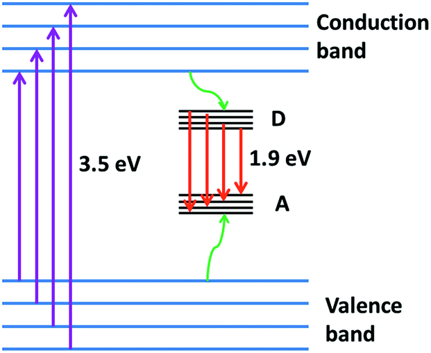 | ||
| Fig. 4 Schematic energy-level diagram for the interpretation of orange PL. D: donor, A: acceptor. The effect of size distribution of Si nanocrystals on the bandgap energy and defect levels is represented by the series of lines. The green arrows stand for the capture of electrons and holes by donors and acceptors. | ||
The bandgap of the porous Si nanowires deserves some discussion. The size distribution of Si nanocrystals is evidenced by high-resolution TEM image (Fig. S4†). The nanocrystal size varies from ∼2 nm to >10 nm. Due to the relative small Bohr radius of Si, it is hard to achieve strong quantum confinement. Therefore, the bandgap would not increase a lot when the nanocrystal size decreases. It was reported that the bandgap is around 1.5 eV when the nanowire size is 2–3 nm.30 To obtain information of bandgap, we also measured the absorption spectrum of porous Si nanowires (Fig. S5†). The spectrum shows edge-like but broad absorption in the 1.1–2.5 eV region, and it is difficult to extract the value of bandgap. However, we suggest that the absorption is likely due to indirect bandgap transition, while the transition resulting in the PL is the direct one. This is supported by the PLE spectrum (Fig. 3a), which shows the onset of effective excitation around 2.5 eV and a large Stokes shift of ∼1.5 eV. Unfortunately, clear transition around 3.5 eV is smeared due to the size distribution and possible band structure change of the Si nanocrystals.
Currently the chemical nature of the donor and acceptor centers involved in the PL is unclear. Firstly, we note that the residual Ag can hardly affect the PL properties although it may act as deep levels in silicon. This is because during the etching Ag is a catalyst rather than dopant, and the in-diffusion of Ag should be very weak at such low etching temperature. Secondly, since the porous nanowires stem from heavy p-type Si wafer, the role of initial doping also deserves some discussion. For this sake we prepared porous Si nanowires from n-type Si wafer and measured their PL properties (see Fig. S2 in ESI†). The n-type nanowires show PL with very similar peak energy and linewidth to the p-type nanowires. Moreover, the PL intensity also shows power-law dependence on the excitation density with a slope of ∼0.85, and a saturation effect in higher-excitation regime. These results strongly suggest that the PL in n-type porous Si nanowires is also defect in nature, and the initial doping is unlikely responsible for the donor/acceptor involved in the transitions. Therefore, it seems that surface defects/states are candidates for the orange PL as suggested in the literature.12 In the porous nanowires prepared by chemical etching, there might be many kinds of surface states locating at different sites, including hydrogen-related bonds, oxidation states and etching-created defects in the Si lattice. In a previous work, we found that surface passivation by dielectric oxides can improve the PL of porous Si nanowires. It suggests that at least some surface states act as carrier traps and are not likely donors or acceptors involved in the PL. It is reasonable to assume that the specific surface at the porous site or not will behave differently. Therefore, further studies on the delicate control of surface chemistry and characterization of those surface states are necessary to the better understanding of the luminescence mechanism in such porous Si nanowires.
Conclusions
In summary, we carried out excitation density-dependent PL and wavelength-dependent PL decay to study the origin of PL from porous Si nanowires. The PL intensity shows sub-unity power function of the excitation density. The PL energy blueshifts with increasing excitation density, and the PL lifetime decreases with increasing luminescence energy. These results unambiguously indicate that the orange PL from porous Si nanowires is due to DAP recombination. The blueshift of PL with increasing excitation energy suggests that quantum confinement effect also plays roles in the PL. The results obtained in porous Si nanowires may shed new light upon the luminescence mechanism of Si nanostructures with other morphologies.Acknowledgements
This work was supported by the Natural Science Foundation of China (No. 51372223), Program for Innovative Research Team in University of Ministry of Education of China (No. IRT13037), and the Fundamental Research Funds for the Central Universities (No. 2014FZA4008).Notes and references
- A. G. Cullis and L. T. Canham, Nature, 1991, 353, 335 CrossRef CAS PubMed.
- M. J. Sailor and E. C. Wu, Adv. Funct. Mater., 2009, 19, 3195 CrossRef CAS PubMed.
- Z. H. Kang, Y. Liu and S. T. Lee, Nanoscale, 2011, 3, 777 RSC.
- A. Sa'ar, J. Nanophotonics, 2009, 3, 032501 CrossRef PubMed.
- N. A. Harun, B. R. Horrocks and D. A. Fulton, Chem. Commun., 2014, 50, 12389 RSC.
- M. Dasog, G. B. de los Reyes, L. V. Titova, F. A. Hegmann and J. G. C. Veinot, ACS Nano, 2014, 8, 9636 CrossRef CAS PubMed.
- J. R. Chen, D. C. Wang, H. C. Hao and M. Lu, Appl. Phys. Lett., 2014, 104, 061105 CrossRef PubMed.
- Y. L. Li, B. Qian, Z. P. Sui and C. P. Jiang, Appl. Phys. Lett., 2013, 103, 161908 CrossRef PubMed.
- W. D. A. M. de Boer, D. Timmerman, K. Dohnalova, I. N. Yassievich, H. Zhang, W. J. Buma and T. Gregorkiewicz, Nat. Nanotechnol., 2010, 5, 878 CrossRef CAS PubMed.
- J. Valenta, B. Bruhn and J. Linnros, Nano Lett., 2011, 11, 3003 CrossRef CAS PubMed.
- A. G. Cullis, L. T. Canham and P. D. J. Calcott, J. Appl. Phys., 1997, 82, 909 CrossRef CAS PubMed.
- S. M. Prokes, W. E. Carlos and O. J. Glembocki, Phys. Rev. B: Condens. Matter Mater. Phys., 1994, 50, 17093 CrossRef CAS.
- H. Haick, P. T. Hurley, A. I. Hochbaum, P. D. Yang and N. S. Lewis, J. Am. Chem. Soc., 2006, 128, 8990 CrossRef CAS PubMed.
- Z. H. Kang, Y. Liu, C. H. A. Tsang, D. D. D. Ma, X. Fan, N. B. Wong and S. T. Lee, Adv. Mater., 2009, 21, 661 CrossRef CAS PubMed.
- L. W. Sun, H. P. He, C. Liu, Y. F. Lu and Z. Z. Ye, CrystEngComm, 2011, 13, 2439 RSC.
- X. T. Lu, C. M. Hessel, Y. X. Yu, T. D. Bogart and B. A. Korgel, Nano Lett., 2013, 13, 3101 CrossRef CAS PubMed.
- K. Q. Peng, A. J. Lu, R. Q. Zhang and S. T. Lee, Adv. Funct. Mater., 2008, 18, 3026 CrossRef CAS PubMed.
- A. I. Hochbaum, D. Gargas, Y. J. Hwang and P. D. Yang, Nano Lett., 2009, 9, 3550 CrossRef CAS PubMed.
- Y. Q. Qu, L. Liao, Y. J. Li, H. Zhang, Y. Huang and X. F. Duan, Nano Lett., 2009, 9, 4539 CrossRef CAS PubMed.
- E. Mulazimoglu, G. Nogay, R. Turan and H. E. Unalan, Appl. Phys. Lett., 2013, 103, 143124 CrossRef PubMed.
- L. Gan, L. W. Sun, H. P. He and Z. Z. Ye, J. Mater. Chem. C, 2014, 2, 2668 RSC.
- H. P. He, C. Liu, L. W. Sun and Z. Z. Ye, Appl. Phys. Lett., 2011, 99, 123106 CrossRef PubMed.
- T. Schmidt and K. Lischka, Phys. Rev. B: Condens. Matter Mater. Phys., 1992, 45, 8989 CrossRef.
- B. V. Kamenev and A. G. Nassiopoulou, J. Appl. Phys., 2001, 90, 5735 CrossRef CAS PubMed.
- K. Tamura, T. Makino, A. Tsukazaki, M. Sumiya, S. Fuke, T. Furumochi, M. Lippmaa, C. H. Chia, Y. Segawa, H. Koinuma and M. Kawasaki, Solid State Commun., 2003, 127, 265 CrossRef CAS.
- D. G. Thomas, J. J. Hopfield and W. M. Augustyniak, Phys. Rev., 1965, 140, A202 CrossRef.
- B. P. Zhang, N. T. Binh, Y. Segawa, Y. Kashiwaba and K. Haga, Appl. Phys. Lett., 2004, 84, 586 CrossRef CAS PubMed.
- U. Kim, I. Kim, Y. Park, K. Y. Lee, S. Y. Yim, J. G. Park, H. G. Ahn, S. H. Park and H. J. Choi, ACS Nano, 2011, 5, 2176 CrossRef CAS PubMed.
- J. P. Wilcoxon, G. A. Samara and P. N. Provencio, Phys. Rev. B: Condens. Matter Mater. Phys., 1999, 60, 2704 CrossRef CAS.
- M. Nolan, S. O'Callaghan, G. Fagas, J. C. Greer and T. Frauenheim, Nano Lett., 2007, 7, 34 CrossRef CAS PubMed.
Footnote |
| † Electronic supplementary information (ESI) available: Excitation-intensity dependent PL spectra of porous Si NWs under excitation of a pulsed laser. See DOI: 10.1039/c5ra13820e |
| This journal is © The Royal Society of Chemistry 2015 |