Horizontal growth of MoS2 nanowires by chemical vapour deposition
Shuming Hana,
Cailei Yuan*a,
Xingfang Luo*a,
Yingjie Caoa,
Ting Yua,
Yong Yanga,
Qinliang Lia and
Shuangli Yeb
aJiangxi Key Laboratory of Nanomaterials and Sensors, Jiangxi Key Laboratory of Photoelectronics and Telecommunication, School of Physics, Communication and Electronics, Jiangxi Normal University, Nanchang 330022, Jiangxi, China. E-mail: clyuan@jxnu.edu.cn; xfluo@jxnu.edu.cn
bSchool of Printing and Packaging, Wuhan University, Wuhan 430072, Hubei, China
First published on 6th August 2015
Abstract
We describe a single step route for the synthesis of MoS2 wires using a chemical vapour deposition (CVD) method. By tuning the CVD growth parameters, the horizontally oriented MoS2 nanowires on SiO2/Si substrate can be synthesized successfully. The MoS2 nanowire has height of about 93 nm and width of about 402 nm with multilayer structure. Good local photoluminescence (PL) properties can be observed for these horizontal MoS2 nanowires. The successful fabrication and prominent PL effect of the horizontal MoS2 nanowires provide potential applications for the MoS2-based in planar devices.
Introduction
Extensive attention has been paid to the field of nanofabrication due to its huge number of potential applications in future nanodevice technology. Two major concerns which need to be addressed for practical applications are the synthesis of useful nanomaterials and the assembly of the synthesized nanostructures on the substrate with desired orientations.On the other hand, semiconductor nanowires have attracted scientific and technological interest owing to their demonstrated potential for high-performance nanoscale devices such as transistors,1 sensors,2 solar cells,3 and thermoelectric systems.4 The ultra-thin bodies of nanowires allow excellent electrostatic control which is required for high performance electronic devices. The one-dimensional (1D) morphology of nanowires enables straightforward implementation of semicylindrical gate or gate-all-around architectures. Wafer-scale integration with current planar processing technology remains a challenge for the commonly grown out-of-plane nanowire geometry. Ex situ assembly methods are required to transfer and coarsely align the nanowires in plane on a functional device substrate.5,6 Therefore, in order to extend the device integrations and viable applications of nanowires, deterministic fabrication method for horizontal growth of nanowires is also required for planar devices.7
MoS2, a typical and the most abundant semiconductor materials, owns a structure of S–Mo–S stacking layers, weakly bounded by van der Waals interactions. The band structure of MoS2 varies with the number of layer. With the layer number decreasing, the lowest band in the conduction band moves upward, increasing the overall bandgap,8 making it advantageous compared to graphene-based logic device applications.9 Moreover, the optical properties of layered materials are strongly dependent on morphology and quality of pristine materials.10,11 Efforts have been made in developing reliable and flexible approaches for obtaining thin layer MoS2 (ref. 12–14) or 1D nanostructures of MoS2 such as nanotubes,15 nanoribbons16 and nanorods.17 In this paper, a simple and precise method to synthesize horizontal growth of MoS2 nanowires has been proposed, which can provide new opportunities for further widespread applications of MoS2-based in planar devices.
Experimental
In this paper, we report horizontal growth of MoS2 nanowires on SiO2/Si substrate by chemical vapour deposition (CVD), as shown in Fig. 1. Briefly, a two temperature zone tube furnace was used to provide accurate temperature control of the solid MoO3 and sulfur (S), respectively. An alumina boat with S powders (99.9% purity) was placed upstream in the low-temperature zone. Another alumina boat containing MoO3 (99.9% purity) was placed downstream in the high-temperature zone. A piece of Si wafer with 300 nm SiO2 layer substrate was placed face down to the MoO3 powder. The distance between these two alumina boats is 19 cm. The temperature of S and the substrate was increased concurrently to 200 °C and 750 °C in the Ar flow atmosphere, respectively. The deposition process was conducted by evaporating S and MoO3 powders simultaneously with the stoichiometric S to Mo ratio of 4![[thin space (1/6-em)]](https://www.rsc.org/images/entities/char_2009.gif) :
:![[thin space (1/6-em)]](https://www.rsc.org/images/entities/char_2009.gif) 1 in Ar flow rate of 30 sccm. After 1 minute, the furnace was cooled down naturally to room temperature. The sample structure was examined by using a Rigaku X-ray diffractometer (XRD) with Cu Kα radiation. The morphology of the MoS2 nanowires was examined by using Park system atomic force microscopy (AFM). Raman spectra were collected by a Horiba Jobin Yvon Raman microscopic system. The solid-state excitation laser has a wavelength of 532 nm. A 100× objective was used to focus the laser beam. The photoluminescence (PL) measurements were also performed with the same laser by using the PL mode of the Raman microscopic system.
1 in Ar flow rate of 30 sccm. After 1 minute, the furnace was cooled down naturally to room temperature. The sample structure was examined by using a Rigaku X-ray diffractometer (XRD) with Cu Kα radiation. The morphology of the MoS2 nanowires was examined by using Park system atomic force microscopy (AFM). Raman spectra were collected by a Horiba Jobin Yvon Raman microscopic system. The solid-state excitation laser has a wavelength of 532 nm. A 100× objective was used to focus the laser beam. The photoluminescence (PL) measurements were also performed with the same laser by using the PL mode of the Raman microscopic system.
Results and discussion
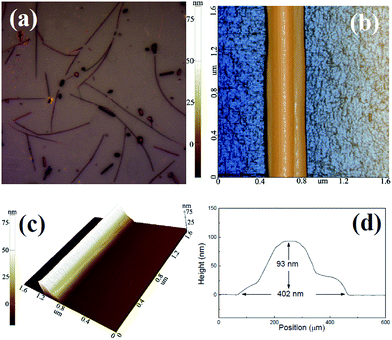
The optical image of MoS2 nanowires on the SiO2/Si substrate synthesized by this CVD system with pure Ar carrier gas flow rate of 30 sccm is presented in Fig. 2(a). The darker-contrast nanowires on the surface signify the MoS2 nanowires, and the surrounding regions correspond to the SiO2/Si substrate. A lot of nanowires are clearly visible over the surface of the substrate. Fig. 2(b) illustrates the morphology of MoS2 nanowire by AFM measurements. A well-defined wire-like structure of MoS2 wire can be observed clearly. Fig. 2(c) is the cross sectional AFM images of MoS2 wires on the SiO2/Si substrate. The height profile of this MoS2 nanowire is shown in Fig. 2(d). From the height profile, it can be found that the MoS2 nanowire has the height of about ∼93 nm and width of about ∼402 nm. Our previous works also demonstrated that the physical properties and morphologies of MoS2 can be controlled by adjusting the chemical environment during growth.18,19 Here, the MoS2 nanowires are synthesized by evaporating S and MoO3 powders simultaneously with the stoichiometric S to Mo ratio of 4![[thin space (1/6-em)]](https://www.rsc.org/images/entities/char_2009.gif) :
:![[thin space (1/6-em)]](https://www.rsc.org/images/entities/char_2009.gif) 1 in Ar flow rate of 30 sccm. The higher partial pressure of gaseous S greatly increases the volatilization speed of MoO3, forming a large amount of gaseous intermediate MoO3−x in a short time.20 Therefore, the high S sufficient atmosphere may promote the mass transfer process, which contributes to the increase in the crystal growth rate. Under the S sufficient atmosphere condition, the MoS2 crystals are more likely to grow under “kinetic” conditions rather than thermodynamic ones, which is typical for nanocrystals with high precursor feedstock. Therefore, the increase in precursor concentration has an effect of promoting the crystal growth rate, resulting in the formation of MoS2 nanowire, which is not favorable for the production of high-quality two-dimensional crystal.18,19
1 in Ar flow rate of 30 sccm. The higher partial pressure of gaseous S greatly increases the volatilization speed of MoO3, forming a large amount of gaseous intermediate MoO3−x in a short time.20 Therefore, the high S sufficient atmosphere may promote the mass transfer process, which contributes to the increase in the crystal growth rate. Under the S sufficient atmosphere condition, the MoS2 crystals are more likely to grow under “kinetic” conditions rather than thermodynamic ones, which is typical for nanocrystals with high precursor feedstock. Therefore, the increase in precursor concentration has an effect of promoting the crystal growth rate, resulting in the formation of MoS2 nanowire, which is not favorable for the production of high-quality two-dimensional crystal.18,19
 | ||
| Fig. 2 (a) Optical microscope image for MoS2 nanowires deposited on SiO2/Si substrate; (b) and (c) a typical AFM image for MoS2 nanowire; (d) height profile for MoS2 nanowire. | ||
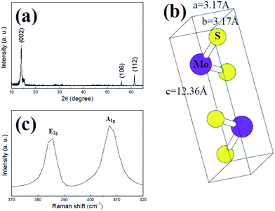
In order to clarify the structure and quality of the MoS2 nanowires, XRD and Raman spectroscopy measurements had been performed. Fig. 3(a) shows the XRD pattern of MoS2 nanowires deposited on SiO2/Si substrate. No diffraction peaks from impurities are observed in the XRD pattern. All the diffraction peaks in the pattern can be indexed as hexagonal-phase MoS2. Moreover, the XRD pattern is matched against a simulated XRD pattern generated by using Java Electron Microscopy Simulation (JEMS) software.21 As shown in Fig. 3(b), the lattice constants of MoS2 calculated from this XRD pattern are a = b = 3.17 Å and c = 12.36 Å. It shows an obvious increase in comparison with the standard values of MoS2 (a = b = 3.16 Å, c = 12.29 Å). The results indicate that the distance between neighbouring MoS2 layers increases and the in-plane structure of MoS2 is slightly changed. The slight change in MoS2 nanostructures might be associated with the defects formed in the growth of MoS2 nanowires. Fig. 3(b) shows the Raman spectra of MoS2 nanowires. It can be found that the two characteristic Raman vibration modes E2g and A1g can be seen in the spectra of MoS2 nanowires. The E2g mode is associated with the in-plane vibrations, i.e., two S atoms are displaced in one direction and the Mo atom is displaced in the opposite direction. The A1g mode is related to the perpendicular vibrations, i.e., two S atoms are displaced in opposite directions while the Mo atom does not move. These two Raman modes, E2g and A1g, exhibit a sensitive layer thickness dependence,22 which provides convenient and reliable means for determining the layer thickness with atomic precision. Due to the alterations in the interlayer coupling,23 the Raman frequency of the former decreases and that of the latter increases with the increasing thickness. It can be found that the in-plane E2g and out-of-plane A1g modes of vibration are at 384 cm−1 and 408 cm−1 for the MoS2 nanowires on the SiO2/Si substrate, respectively. A Δ of 24 cm−1 between these two modes suggests the fabricated MoS2 nanowires are the multilayers structure.
 | ||
| Fig. 3 (a) XRD patterns of MoS2 nanowires; (b) schematic image of MoS2 unit cells; (c) typical Raman spectra of MoS2 nanowires. | ||
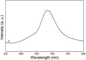
Fig. 4 presents the PL spectrum for the MoS2 nanowires with 532 nm laser source at room temperature. PL measurements were performed with the same laser excitation source and conditions as that for Raman spectroscopy. In contrast to the silent PL effect of the bulk MoS2 indirect semiconductor, two strong peaks can be found in the PL spectrum for the MoS2 nanowires, 684 nm and 631 nm. The PL emission of the MoS2 nanorods could be related to the transition of PL emission process from trion recombination to exciton recombination, which is assisted with the defects in the materials.24 Because the MoS2 nanowires are synthesized in high S sufficient atmosphere with the stoichiometric S to Mo ratio of 4![[thin space (1/6-em)]](https://www.rsc.org/images/entities/char_2009.gif) :
:![[thin space (1/6-em)]](https://www.rsc.org/images/entities/char_2009.gif) 1, under the S sufficient atmosphere condition, the MoS2 crystals are more likely to grow under “kinetic” conditions rather than thermodynamic ones. In this case, instability may occur as atoms do not have enough time to move into the right lattice locations, where crystal domains could have the lowest surface free energy, and the probability of defect formation increases. Therefore, there could be many defects formed in the MoS2 nanowires. The excitons localized at the defect sites generally have much larger binding energy,25,26 which may suppress the thermally activated nonradiative recombination including defect trapping, and resulting in the observed PL properties.
1, under the S sufficient atmosphere condition, the MoS2 crystals are more likely to grow under “kinetic” conditions rather than thermodynamic ones. In this case, instability may occur as atoms do not have enough time to move into the right lattice locations, where crystal domains could have the lowest surface free energy, and the probability of defect formation increases. Therefore, there could be many defects formed in the MoS2 nanowires. The excitons localized at the defect sites generally have much larger binding energy,25,26 which may suppress the thermally activated nonradiative recombination including defect trapping, and resulting in the observed PL properties.
Conclusion
It is meaningful to develop a sample and precise method to synthesize horizontal MoS2 nanowires for planar device application. In this paper, we report horizontal growth of MoS2 nanowires on SiO2/Si substrate by CVD. The MoS2 nanowire has height of about 93 nm and width of about 402 nm. Good local PL properties of MoS2 nanowires can be observed. The successful fabrication and prominent PL effect of the horizontal MoS2 nanowires provide potential applications for the MoS2-based in planar devices.Acknowledgements
This work is supported by National Natural Science Foundation of China (Grant Nos 11164008, 51461019, 51361013, 11174226, and 51371129), the Project for Young Scientist Training of Jiangxi Province (20153BCB23016) and the Natural Science Foundation of Jiangxi Province (20151BAB202004).Notes and references
- S. C. Hung, W. Y. Woon, S. M. Lan, F. Ren and S. J. Pearton, Appl. Phys. Lett., 2013, 103, 083506 CrossRef PubMed.
- L. Z. Du, Y. H. Zhang, Y. A. Lei and H. P. Zhao, Mater. Lett., 2014, 129, 46 CrossRef CAS PubMed.
- M. Kim, J. H. Park, J. H. Kim, J. H. Sung, S. B. Jo, M. H. Jo and K. Cho, Adv. Energy Mater., 2015, 5, 1401317 Search PubMed.
- E. Z. Xu, Z. Li, J. A. Martinez, N. Sinitsyn, H. Htoon, N. Li, B. Swartzentruber, J. A. Hollingsworth, J. Wang and S. X. Zhang, Nanoscale, 2015, 7, 2869 RSC.
- S. A. Fortuna, J. G. Wen, I. S. Chun and X. L. Li, Nano Lett., 2008, 8, 4422 CrossRef PubMed.
- Y. L. Zi, K. Jung, D. Zakharo and C. Yang, Nano Lett., 2013, 13, 2786 CrossRef CAS PubMed.
- J. Kim, H. Jeong and J. Y. Park, Curr. Appl. Phys., 2013, 13, 425 CrossRef PubMed.
- M. Chhowalla, H. S. Shin, G. Eda, L. J. Li, K. P. Loh and H. Zhang, Nat. Chem., 2013, 5, 263 CrossRef PubMed.
- B. Radisavljevic, A. Radenovic, J. Brivio, V. Giacometti and A. Kis, Nat. Nanotechnol., 2011, 6, 147 CrossRef CAS PubMed.
- S. X. Yang, Y. Li, X. Z. Wang, N. J. Huo, J. B. Xia, S. S. Li and J. B. Li, Nanoscale, 2014, 6, 2582 RSC.
- S. X. Yang, S. Tongay, Q. Yue, Y. T. Li, B. Li and F. Y. Lu, Sci. Rep., 2014, 4, 5442 CAS.
- S. S. Wang, Y. M. Rong, Y. Fan, M. Pacios, H. Bhaskaran, K. He and J. H. Warner, Chem. Mater., 2014, 26, 6371 CrossRef CAS.
- B. Li, S. X. Yang, N. J. Huo, Y. T. Li, J. H. Yang, R. X. Li, C. Fan and F. Y. Lu, RSC Adv., 2014, 4, 26407 RSC.
- S. Y. Yang, J. Kang, Q. Yue and K. Yao, J. Phys. Chem. C, 2014, 118, 9203 CAS.
- S. F. Zhuo, Y. Xu, W. W. Zhao, J. Zhang and B. Zhang, Angew. Chem., Int. Ed., 2013, 52, 8602 CrossRef CAS PubMed.
- S. Fathipour, M. Remskar, A. Varlec, A. Ajoy, R. Yan, S. Vishwanath, S. Rouvimov, W. S. Hwang, H. G. Xing, D. Jena and A. Seabaugh, Appl. Phys. Lett., 2013, 106, 022114 CrossRef PubMed.
- H. T. Lin, X. Y. Chen, H. L. Li, M. Yang and Y. X. Qi, Mater. Lett., 2010, 64, 1748 CrossRef CAS PubMed.
- Y. J. Cao, X. F. Luo, S. M. Han, C. L. Yuan, Y. Yang, Q. L. Li, T. Yu and S. L. Ye, Chem. Phys. Lett., 2015, 631–632, 30 CrossRef CAS PubMed.
- Y. J. Cao, X. F. Luo, C. L. Yuan, S. M. Han, T. Yu, Y. Yang and Q. L. Li, Phys. E, 2015, 74, 292 CrossRef PubMed.
- L. M. Zhang, K. H. Liu, A. B. Wong, J. Kim, X. P. Hong, C. Liu, T. Cao, S. G. Louie, F. Wang and P. D. Yang, Nano Lett., 2014, 14, 6418 CrossRef CAS PubMed.
- P. A. Stadelmann, Ultramicroscopy, 1987, 21, 131 CrossRef CAS.
- H. Li, Q. Zhang, C. C. R. Yap, B. K. Tay, T. H. T. Edwin, A. Olivier and D. Baillargeat, Adv. Funct. Mater., 2012, 22, 1385 CrossRef CAS PubMed.
- Y. C. Cheng, Z. Y. Zhu and U. Schwingenschlögl, RSC Adv., 2012, 2, 7798 RSC.
- H. Y. Nan, Z. L. Wang, W. H. Wang, Z. Liang, Y. Lu, Q. Chen, D. W. He, P. H. Tan, F. Miao, X. R. Wang, J. L. Wang and Z. H. Ni, ACS Nano, 2014, 8, 5738 CrossRef CAS PubMed.
- L. Wirtz, A. Marini and A. Rubio, Phys. Rev. Lett., 2006, 96, 126104 CrossRef.
- S. D. Wang, Q. Chen and J. L. Wang, Appl. Phys. Lett., 2011, 99, 063114 CrossRef PubMed.
| This journal is © The Royal Society of Chemistry 2015 |


