Chemical control of continuous light-steering using an array of gradient Au/Bi2Se3/Au strips
Tun Cao*,
Guangzhao Zheng and
Shuai Wang
Department of Biomedical Engineering, Dalian University of Technology, Dalian 116024, China. E-mail: caotun1806@dlut.edu.cn
First published on 10th August 2015
Abstract
Light-steering devices have been extensively investigated for a large host of applications in defense, communications, data storage and display technologies. However, the challenge is to continuously steer the light over a wide angular range in the optical region, using actively tunable structure with a small footprint. Here, we numerically demonstrate a gradient phase-array-like Au/Bi2Se3/Au trilayers plasmonic resonators for actively steering the beam in the near-infrared (N-IR) region. The proposed device provides a continuously large beam-steering of 18° for the reflected light and 9° for the transmitted light around the resonant wavelength of 1500 nm by changing the state of Bi2Se3 from amorphous to crystalline. The essence of this phenomenon lies in the variation of refractive index of Bi2Se3 induced by the phase transition, which is achieved through the chemical reactions between the Bi2Se3 film and AgNO3 solution. The continuous beam-steering is enabled by gradually increasing the immersion time (tim) of the Bi2Se3 into AgNO3 solution. This study exploits a new research area of Bi2Se3 based nano-antenna for dynamic optical routing and switching in photonic circuits.
1 Introduction
On-chip optical antennas array represents an enabling technology that makes fast, straightforward, and lightweight laser beam-steering with precise stabilization, random access pointing and programmable multiple simultaneous beams.1–3 This would greatly impact optical communication, holographic video displays, and laser ranging and detection.4–7 Such optical antennas array can steer and shape light efficiently by controlling the phase of each antenna element.8 The phase control of the optical antennas array can be obtained by optimizing the geometry and location of the antenna elements, so called as passive antennas array.9–13 Yet in order to achieve the required phase, designers have to carefully consider the pattern, arrangement, coupling between resonators as well as nanofabrication tolerance of the passive nano-antennas array. This makes packaging challenging and increases the complexity of the device. To solve the problem, active control of the propagation direction of beam has been extensively investigated and became the very heart of the beam-steering technology.14 For example, on-chip optical phased arrays (OPAs) based on gratings have been proposed to actively steer the beam using frequency tuning.15,16 Although these grating based OPAs have a good steering performance, the tunable frequency limits their applications in the field of free-space communication link and sensing.7 Recently, OPAs integrated with various active elements, i.e. liquid crystals (LCs),17 active silicon,14 thermally reconfigurable semiconductors18 and phase changed materials (PCMs),8 have been approached to provide an active beam-steering with low cost and simple mechanical systems. The key element of this technology is to modify the phase of OPAs by tuning the refractive index of the electro-optical material, and thus controlling direction and divergence of light at a fixed frequency. Despite the substantial progress in active OPAs, it is still a formidable challenge to continuously steer the beam over a wide angular range in the near-infrared (N-IR) region. For example, the beam-steering devices using OPAs integrated with active semiconductors are normally designed to operate at the wavelength of 10 μm.14,18 However, little research has been done on actively steering the direction of the incident light at the shorter wavelength region. That is because the semiconductors do not sustain high densities of injected free electrons outside the THz frequency range, especially from the visible to N-IR regions.19 Therefore, implementation of beam-steering using OPAs in the N-IR region is desirable, considering their applications in the field of optical communication. Meanwhile, the continuous beam-steering is often necessary for a rich variety of new and exciting areas i.e. automotive applications.1,6 Moreover, the integration of the electrodes for tuning active dielectric materials restricts the scaling of OPAs and may be difficult to be realized by the current nanofabrication techniques. Therefore, an appealing route that is particular for active nano-antennas array is to chemically tune the optical properties of the structure without using large bulky electrodes.20,21Topological insulator (TI), a new class of Dirac material, has attracted great interests in recent years.22–25 It is a potential candidate for high performance optical devices such as photodetectors, terahertz lasers, rewriteable optical data storage, photonic circuitry that is less dependent on isolators and slow light that is insensitive to disorder.26,27 BixSb1−x, Bi2Se3, and Bi2Te3 compounds are shown to be TIs using angle-resolved photoemission spectroscopy (ARPES),28–33 where Bi2Se3 is particularly interesting since it has a relatively large bulk band gap and simple surface state consisting of a single Dirac cone-like structure.30,34 Recently, experiments have revealed that the optical dielectric constant of Bi2Se3 can be very different in the N-IR region as transiting its state between crystalline and amorphous.35 In this context, we envisage the possibility of continuously steering the light by using gradient phase-array-like metal/dielectric/metal (MDM) multilayer strips, where Bi2Se3 is selected as the dielectric interlayer.
Here, an array of gradient Au/Bi2Se3/Au tri-layer strips is proposed to continuously control the propagation direction of incident light over a wide angle in the N-IR region. As two metal layers are placed closer than the surface plasmon polaritons (SPPs) attenuation length, the SPPs propagating along each of the two metal–dielectric interfaces of the MDM structures can couple to each other hence providing a very strong localization of light inside the internal dielectric layer.36 By introducing Bi2Se3 into the MDM structure as a dielectric interlayer, the tunable resonant characteristics of the structure can be realized by switching between two states of Bi2Se3, where the phase transition can be obtained through the chemical reactions between the Bi2Se3 film and AgNO3 solution.35 The variation in refractive index of the amorphous and crystalline state of Bi2Se3 will change the intrinsic effective dielectric properties of the MDM structure.37 Therefore, the MDM strips array integrated with Bi2Se3 can be used as actively controlled phase shifters for beam-steering device. Moreover, it is hypothesized that a continuous beam-steering can be obtained by immersing Bi2Se3 in AgNO3 solution for different periods of time. It is because that Bi2Se3 film is amorphous in nature while those immersed in the AgNO3 solution are crystalline. By increasing immersion time (tim), the Bi2Se3 dielectric layer can be gradually crystallized hence continuously steering the reflected light over a 18° (from 72° to 90°) angular range and transmitted light over a 9° (from 264° to 273°) angular range around the resonance wavelength of 1500 nm, respectively.
Reversibly transiting the state of Bi2Se3 may sound challenging. To address this problem, we suggest that a future design, with improved cycleability, should include a possibility of the crystalline Ag2Se transforming into the amorphous Bi2Se3 through cation exchange reaction.38 The low crystallization activation energy of 1.32 eV of the Bi2Se3 may effect the stability of its amorphous phase.39 However, new phase change materials, that may switch between two crystalline states without melting, such as interfacial phase change materials (IPCMs), should be used.40 Although the tunable resonance of the plasmonic structure in one way limits its applications, it can be a potential candidate for a write-once device and thus still attracting much attention. For example, adjusting of the structural parameters to obtain the tunable metamaterials (MMs) has been widely studied.41–44 Particularly, García-Meca et al. demonstrated that one can tune the permeability of the multilayer fishnet MMs by changing the lattice constant of the structure.41 The effective optical parameters of these MMs can only be tuned in one way since it is hard to change the geometry size of resonators in the metamaterials once they are fabricated.
Meanwhile, capillary action in the MDM strips array leads to an efficient reaction between the Bi2Se3 film and AgNO3 solution.45 Compared to the electrical controlled active beam-steering devices, our approach to demonstrate a chemically controlled optical beam-steering device can remove large bulky electrodes and thus considerably reducing size, weight and power requirements. The structure possesses a simple geometry which can be fabricated using standard photolithography patterning. Finally, it should be noted that Bi2Se3 does not require any energy to maintain the structural state of the material. Thus, once the device has been switched it will retain the beam direction until it is switched again. This obviously makes the proposed beam-steering design interesting from a ‘green technology’ perspective.
2 Results and discussions
Structure and design
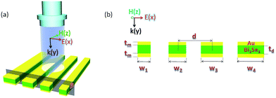
Fig. 1a shows an array of four gradient MDM multilayer resonators suspended in a vacuum. Each resonator consists of a sandwiched Bi2Se3 dielectric interlayer between a top and bottom Au film. Au is selected as the metal due to its stability and low ohmic loss. The thicknesses of the Au/Bi2Se3/Au trilayers are at 20/140/20 nm. The MDM multilayer strips are assumed infinite along the z direction and β is a cross-section plane of the structure (x–y plane). The geometry of the structure is optimized for the maximum sensitivity of the beam-steering angle to a change in the refractive index of the Bi2Se3 layer at λ = 1500 nm. The center to center distance between each element is d = 600 nm. A finite-width MDM strip represents a plasmonic resonator, in which the counter propagating SPPs at the top and bottom metal–dielectric interfaces are efficiently reflected by the ends of the strip. It can form a resonant standing-wave pattern hence localizing the light within the dielectric interlayer when the counter-propagating SPPs interfere constructively. The resonance condition is given by| k0neffw = mπ + φ | (1) |
 is the wave vector of the incident light, neff is the effective refractive index of the MDM strip, w is the width of the strip, m is an integer, and φ is a reflection phase at the end of the strip.14,37,46 For amorphous Bi2Se3, neff is 3.42 at λ = 1500 nm derived from the explicit dispersion relation in ref. 37. The w is then calculated to be 190 nm using eqn (1), where m = 1 for a first-order resonance. By adding a 20 nm width step on the resonance value of 190 nm, one can obtain four gradient MDM strips with different widths of w1 = 190, w2 = 210, w3 = 230 and w4 = 250 nm. These variously wide MDM resonators can come up with different phase shifts. The structure is simulated by a commercial software (Lumerical FDTD Solutions), which is based on the Finite Difference Time Domain (FDTD) method. The dielectric properties of Au as given by Johnson & Christy are used.47 The structure is excited by a plane wave source at a central wavelength of 1500 nm, propagating along the positive y direction with the electric-field vector (E) polarized in the x direction. Perfectly match layer (PML) absorbing boundaries are applied for all directions. A uniform FDTD mesh size is adopted, the mesh size is the same along all Cartesian axes: Δx = Δy = 2 nm, which is sufficient to minimize the numerical errors arising from the FDTD method. A near-to-far field transformation within Lumerical FDTD has then been used to calculate the far field radiation pattern of the structure.48,49
The Bi2Se3 is a promising candidate to realize modulation functionality since its optical properties dramatically change in the N-IR regime for different tim of the Bi2Se3 in the AgNO3 solution. Due to an ion exchange process in the AgNO3 solution, the substitution of Bi by Ag occurs according to the following chemical reactions:
| Bi = Bi3+ + 3e−, Ag+ + e− = Ag | (2) |
| 2Bi + 3Se2− + 6Ag = 3Ag2Se + 2Bi3+ | (3) |
At the beginning of doping, Ag enters into the interstitial sites in the crystal lattice of the Bi2Se3. However, with further increase of Ag addition such that increase the tim, the interstitial site occupation increases attaining saturation, thus the extra Ag atoms occupy the place of Bi sites in the Bi2Se3 lattice. This leads to a decrease of the optical energy band gap (Eg) of the Bi2Se3 lattice. Namely, increasing the tim leads to the decrease of the Eg and increase of the refractive index of Bi2Se3.35 This phenomenon satisfies the definition of the crystallization of the semiconductor chalcogenide: the crystallization of chalcogenide films is accompanied by a decrease in the Eg.50–52 The Bi2Se3 dielectric interlayer can be gradually crystallized by increasing tim. A sufficient tim can lead to a complete phase transition between the amorphous and crystalline states. Therefore, the refractive index of Bi2Se3 can be continuously changed as gradually increasing tim. Fig. 2 shows the refractive index of amorphous Bi2Se3 film (not immersed into the AgNO3, tim = 0 s) as well as those immersed in the AgNO3 solution for different periods of immersion time (tim = 20, 40 and 60 s), followed by annealing in an Ar atmosphere at 437 K for 1 h, are obtained from the published double-beam spectrophotometer spectroscopy data in ref. 35. Herein, annealing the Bi2Se3 film at a temperature of 473 K for 1 h is in aid of diffusing Ag into the Bi2Se3 layer, in order to effectively crystallize the Bi2Se3 film. As can be seen, in the N-IR regime Bi2Se3 shows a pronounced variation in the refractive index during the structural transformation from amorphous (tim = 0 s) to crystalline (tim = 20, 40 and 60 s). With these unique properties, Bi2Se3 is of great interest for actively tunable plasmonics and nanophotonics.
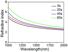 | ||
| Fig. 2 Variation of refractive index vs. wavelength, for the amorphous Bi2Se3 film immersed in AgNO3 solution for different periods of time 0, 20, 40 and 60 s. | ||
Beam-steering using phase-array-like Au/Bi2Se3/Au multilayer strips
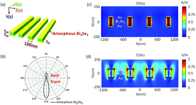
We firstly study the radiation characteristic of four equally wide MDM resonators with amorphous Bi2Se3 shown in Fig. 3a. The width of MDM strip is set to w1 = 190 nm so as to satisfy the interference condition at λ = 1500 nm given in eqn (1) for the first-order resonance (m = 1). Fig. 3b presents the radiation pattern of the MDM strips array under normal incidence. Half-power beam widths (HPBWs) of the front lobe and back lobe are 30° and 34° respectively, where the front and back lobes are symmetrical to the y axis owing to the symmetry in the structure around the y axis. The total magnetic field intensity distribution and total electric field intensity distribution
  along the β plane at λ = 1500 nm are shown in Fig. 3c and d. There is a very strong confinement for both E and H field intensity within the dielectric interlayer and the apertures between the MDM strips, indicating the excitation of the strong SPPs.
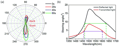
In conventional OPAs, beam is steered by modulating phase shifts between consecutive elements of the array. However, in the array of gradient MDM multilayer strips, the phase shift introduced by each resonator is controlled by changing the refractive index of the dielectric interlayer. The MDM multilayer strips with gradually increasing widths are chosen in order to introduce a different phase shift. Here, we set the width of each MDM multilayer strip as w1 = 190, w2 = 210, w3 = 230 and w4 = 250 nm, respectively. In Fig. 4a, the gradient structures with various refractive index of Bi2Se3 (shown in Fig. 2) are simulated to investigate the effect of the phase change of Bi2Se3 on the beam-steering angles. Compared to the amorphous non-gradient MDM multilayer strips in Fig. 3, the reflected beam (back lobe) and transmitted beam (front lobe) of the amorphous gradient structure (shown in black solid line in Fig. 4a, tim = 0 s) are deflected by 18° and 6° at λ = 1500 nm, respectively. These deflection angles are due to the different phase shift introduced by increasing the width of the element. The HPBWs are 29° and 34° for the front and back lobes, respectively. Active beam-steering can be achieved by switching the phase of Bi2Se3 dielectric interlayer from amorphous to crystalline in the gradient structure. It shows that a continuously angular steering of 9° from 264° to 273° for the transmitted beam (front lobe), as well as 18° from 72° to 90° for the reflected beam (back lobe) at λ = 1500 nm are obtained by increasing the tim. Particularly, a significant angular steering of 18° for the back lobe has a potential of controlling the wavefront of the reflected beam for the possible applications of free-space optical inter/intra chip interconnects.
Moreover, the HPBW only has an increment of 2° for the front lobe and decrement of 1° for the back lobe with the phase transition between amorphous and crystalline. Therefore, the HPBWs are almost independent with the refractive index variation in the Bi2Se3. Fig. 4b shows the beam-steering angles (Δθmax) of both reflected and transmitted light against the central wavelength of the incident light as completely transiting the Bi2Se3 from the amorphous (tim = 0 s) to crystalline (tim = 60 s). As can be seen, a big value of beam-steering angle of more than 9° (4.5°) for the reflected wave (transmitted wave) can be maintained across a full width half maximum (FWHM) of 160 nm (140 nm) in the 1350–1700 nm wavelength.
The mechanism of the continuously active beam-steering is based on the variation in the localization of the incident wave between the MDM multilayer strips.14 Therefore, in order to observe this underlying mechanism, it is instructive to examine the patterns of the H field intensity distribution for the different phases of Bi2Se3 along the cross sectional plane, β, which is shown in Fig. 1a. As can be seen in Fig. 5, the SPPs resonance indicated by H field intensity at λ = 1500 nm gradually increases as decreasing tim since the refractive index of Bi2Se3 is decreased with tim shown in Fig. 2. The H field intensity moves towards wider strips (larger w) to satisfy eqn (1) when tim is decreased (namely, the refractive index of Bi2Se3 is decreased), hence leading to the continuously active beam-steering; the largest deflection angle of 18° in the amorphous gradient structure (tim = 0 s) is due to the fact that SPPs resonance shifts towards wider resonators where the Bi2Se3 exhibits the smallest refractive index at λ = 1500 nm. Here, the H field intensities are normalized to the maximum intensities of the H field in the amorphous non-gradient structure shown in Fig. 3.
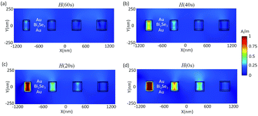 | ||
| Fig. 5 A map of the normalized total magnetic field intensity distribution (H) along the β plane at λ = 1500 nm: (a) tim = 60 s; (b) tim = 40 s; (c) tim = 20 s; (d) tim = 0 s. | ||
3 Discussion
Here, we propose a concept of chemically controlled beam-steering using an array of gradient MDM multilayer strips based on Bi2Se3. The strips with increasing width are chosen to introduce the different phase shift. The transmitted and reflected lights at λ = 1500 nm can be continuously steered from 264° to 273° and 72° to 90° by switching between the amorphous and crystalline state of Bi2Se3, where the phase transition is achieved by immersing Bi2Se3 film in AgNO3 solution for different periods of time. Moreover, the steering angle is stable for spectral changes with a FWHM of 140 nm for the transmitted beam and 160 nm for the reflected beam around λ = 1500 nm. It is expected that chemically controlled tunable plasmonic antenna array based on Bi2Se3 will promise an enormous variety of breakthroughs in technological outcomes and lead to new nanophotonics applications.Acknowledgements
We acknowledge the financial support from National Natural Science Foundation of China (Grant No. 61172059 and 51302026), Ph.D Programs Foundation of Ministry of Education of China (Grant No. 20110041120015), Postdoctoral Gathering Project of Liaoning Province (Grant No. 2011921008), and The Fundamental Research for the Central University (Grant No. DUT14YQ109).Notes and references
- J. Sun, E. Timurdogan, A. Yaacobi, E. S. Hosseini and M. R. Watts, Nature, 2013, 493, 195 CrossRef CAS PubMed.
- S. B. Raghunathan, H. F. Schouten, W. Ubachs, B. Ea Kim, C. H. Gan and T. D. Visser, Phys. Rev. Lett., 2013, 111, 153901 CrossRef CAS.
- D. Kwong, A. Hosseini, J. Covey, Y. Zhang, X. Xu, H. Subbaraman and R. T. Chen, Opt. Lett., 2014, 39, 941 CrossRef CAS PubMed.
- S. Young and B. Schwarz, Opt. Photonics J., 2011, 12, 7 Search PubMed.
- B. Schwarz, Nat. Photonics, 2010, 4, 429 CrossRef CAS PubMed.
- A. Yaacobi, J. Sun, M. Moresco, G. Leake, D. Coolbaugh and M. R. Watts, Opt. Lett., 2014, 39, 4575 CrossRef PubMed.
- C. T. DeRose, R. D. Kekatpure, D. C. Trotter, A. Starbuck, J. R. Wendt, A. Yaacobi, M. R. Watts, U. Chettiar, N. Engheta and P. S. Davids, Opt. Express, 2013, 21, 5198 CrossRef CAS PubMed.
- L. Zou, M. Cryan and M. Klemm, Opt. Express, 2014, 22, 24142 CrossRef CAS PubMed.
- L. Zou, W. Withayachumnankul, C. Shah, A. Mitchell, M. Bhaskaran, S. Sriram and C. Fumeaux, Opt. Express, 2013, 21, 1344 CrossRef PubMed.
- A. Pors, O. Albrektsen, I. P. Radko and S. I. Bozhevolnyi, Sci. Rep., 2013, 3, 2155 Search PubMed.
- Y. Yang, W. Wang, P. Moitra, I. I. Kravchenko, D. P. Briggs and J. Valentine, Nano Lett., 2014, 14, 1394 CrossRef CAS PubMed.
- Y. Yifat, M. Eitan, Z. Iluz, Y. Hanein, A. Boag and J. Scheuer, Nano Lett., 2014, 14, 2485 CrossRef CAS PubMed.
- Z. H. Jiang, L. Lin, J. A. Bossard and D. H. Werner, Opt. Express, 2013, 21, 31492 CrossRef PubMed.
- E. Battal and A. K. Okyay, Opt. Lett., 2013, 38, 983 CrossRef PubMed.
- K. V. Acoleyen, H. Rogier and R. Baets, Opt. Express, 2010, 18, 13655 CrossRef PubMed.
- J. K. Doylend, M. J. R. Heck, J. T. Bovington, J. D. Peters, L. A. Coldren and J. E. Bowers, Opt. Express, 2011, 19, 21595 CrossRef CAS PubMed.
- D. de Ceglia, M. A. Vincenti and M. Scalora, Opt. Lett., 2012, 37, 271 CrossRef PubMed.
- D. C. Adams, S. Thongrattanasiri, T. Ribaudo, V. A. Podolskiy and D. Wasserman, Appl. Phys. Lett., 2010, 96, 201112 CrossRef PubMed.
- P. Y. Yu and M. Cardona, in Fundamentals of semiconductors, ed. H. E. Stanly and W. T. Rhodes, Springer, Berlin, 4th edn, 2004 Search PubMed.
- T. Cao, S. Wang and W. X. Jiang, RSC Adv., 2013, 3, 19474 RSC.
- L. H. Shao, M. Ruther, S. Linden, S. Essig, K. Busch, J. Weissmüller and M. Wegener, Adv. Mater., 2010, 22, 5173 CrossRef CAS PubMed.
- M. Z. Hasan and C. L. Kane, Rev. Mod. Phys., 2010, 82, 3045 CrossRef CAS.
- X. L. Qi and S. C. Zhang, Rev. Mod. Phys., 2011, 83, 1057 CrossRef CAS.
- J. Qi, H. Liu and X. C. Xie, Phys. Rev. B: Condens. Matter Mater. Phys., 2014, 89, 155420 CrossRef.
- J. Y. Ou, J. K. So, G. Adamo, A. Sulaev, L. Wang and N. I. Zheludev, Nat. Commun., 2014, 5, 5139 CrossRef CAS PubMed.
- L. Lu, J. D. Joannopoulos and M. Soljačić, Nat. Photonics, 2014, 8, 821 CrossRef CAS PubMed.
- X. Zhang, J. Wang and S. C. Zhang, Phys. Rev. B: Condens. Matter Mater. Phys., 2010, 82, 245107 CrossRef.
- D. Hsieh, D. Qian, L. Wray, Y. Xia, Y. S. Hor, R. J. Cava and M. Z. Hasan, Nature, 2008, 452, 970 CrossRef CAS PubMed.
- D. Hsieh, Science, 2009, 323, 919 CrossRef CAS PubMed.
- D. Hsieh, Y. Xia, D. Qian, L. Wray, J. H. Dil, F. Meier, J. Osterwalder, L. Patthey, J. G. Checkelsky, N. P. Ong, A. V. Fedorov, H. Lin, A. Bansil, D. Grauer, Y. S. Hor, R. J. Cava and M. Z. Hasan, Nature, 2009, 460, 1101 CrossRef CAS PubMed.
- Y. Xia, D. Qian, D. Hsieh, L. Wray, A. Pal, H. Lin, A. Bansil, D. Grauer, Y. S. Hor, R. J. Cava and M. Z. Hasan, Nat. Phys., 2009, 5, 398 CrossRef CAS PubMed.
- D. Hsieh, Y. Xia, D. Qian, L. Wray, F. Meier, J. H. Dil, J. Osterwalder, L. Patthey, A. V. Fedorov, H. Lin, A. Bansil, D. Grauer, Y. S. Hor, R. J. Cava and M. Z. Hasan, Phys. Rev. Lett., 2009, 103, 146401 CrossRef CAS.
- Y. L. Chen, J. G. Analytis, J.-H. Chu, Z. K. Liu, S.-K. Mo, X. L. Qi, H. J. Zhang, D. H. Lu, X. Dai, Z. Fang, S. C. Zhang, I. R. Fisher, Z. Hussain and Z.-X. Shen, Science, 2009, 325, 178 CrossRef CAS PubMed.
- Z. H. Pan, E. Vescovo, A. V. Fedorov, D. Gardner, Y. S. Lee, S. Chu, G. D. Gu and T. Valla, Phys. Rev. Lett., 2011, 106, 257004 CrossRef.
- G. B. Sakr, I. S. Yahia, G. M. El-Komy and A. M. Salem, Surf. Coat. Technol., 2011, 205, 3553 CrossRef CAS PubMed.
- R. Ortuno, C. Garcia-Meca, F. J. Rodriguez-Fortuno, J. Marti and A. Martinez, Phys. Rev. B: Condens. Matter Mater. Phys., 2009, 79, 075425 CrossRef.
- S. I. Bozhevolnyi and T. Sondergaard, Opt. Express, 2007, 15, 10869 CrossRef CAS.
- G. D. Moon, S. Ko, Y. Min, J. Zeng, Y. Xia and U. Jeong, Nano Today, 2011, 6, 186 CrossRef CAS PubMed.
- D. Nataraj, K. Prabakar, S. K. Narayandass and D. Mangalaraj, Cryst. Res. Technol., 2000, 35, 1087 CrossRef CAS.
- R. E. Simpson, P. Fons, A. V. Kolobov, T. Fukaya, M. Krbal, T. Yagi and J. Tominaga, Nat. Nanotechnol., 2011, 6, 501 CrossRef CAS PubMed.
- C. García-Meca, R. Ortuño, F. J. Rodríguez-Fortuño, J. Martí and A. Martínez, Opt. Lett., 2009, 34, 1603 CrossRef.
- S. Zhang, W. J. Fan, K. J. Malloy, S. R. J. Brueck, N. C. Panoiu and R. M. Osgood, Opt. Express, 2005, 13, 4922 CrossRef.
- G. Dayal and S. A. Ramakrishna, Opt. Express, 2012, 20, 17503 CrossRef CAS PubMed.
- J. Q. Wang, C. Z. Fan, J. N. He, P. Ding, E. J. Liang and Q. Z. Xue, Opt. Express, 2013, 21, 2236 CrossRef PubMed.
- M. Tamura and H. Kagata, IEEE Trans. Microwave Theory Tech., 2010, 58, 3954 CrossRef.
- R. Gordon, Phys. Rev. B: Condens. Matter Mater. Phys., 2006, 73, 153405 CrossRef.
- P. B. Johnson and R. W. Christy, Phys. Rev. B: Condens. Matter Mater. Phys., 1972, 6, 4370 CrossRef CAS.
- J. D. Jackson, Classical Electrodynamics, John Wiley & Sons, 2nd edn, 1975, p. 401 Search PubMed.
- T. Cao, Y. Zou, A. M. Adawi and M. J. Cryan, Opt. Express, 2014, 22, 22699 CrossRef PubMed.
- M. Digiulio, D. Manno, R. Rella, P. Siciliano and A. Tepore, Sol. Energy Mater., 1987, 15, 209 CrossRef CAS.
- M. M. Hafiz, M. A. Abdel-Rahim and A. A. Abu-Sehly, Phys. B, 1998, 252, 207 CrossRef CAS.
- M. M. Hafiz, O. El-Shazly and N. Kinawy, Appl. Surf. Sci., 2001, 171, 231 CrossRef CAS.
| This journal is © The Royal Society of Chemistry 2015 |

