Review on nanomaterials synthesized by vapor transport method: growth and their related applications

X. Xue a, Z. Zhoub, B. Penga, M. M. Zhua, Y. J. Zhanga, W. Rena, Z. G. Yea, X. Chenb and M. Liu*a
aElectronic Materials Research Laboratory, Key Laboratory of the Ministry of Education & International Center for Dielectric Research, Xi'an Jiaotong University, Xi'an 710049, China. E-mail: mingliu@mail.xjtu.edu.cn
bEnergy Systems Division, Argonne National Laboratory, Lemont, IL 60439, USA

Received 8th July 2015 , Accepted 9th September 2015

First published on 9th September 2015


Abstract

Nanostructures with different dimensions, including bulk crystals, thin films, nanowires, nanobelts and nanorods, have received considerable attention due to their novel functionalities and outstanding applications in various areas, such as optics, electricity, thermoelectricity, photovoltaic fields and sensing devices. In recent years, remarkable progresses and modifications have been made upon the fabrication of nanomaterials by vapor transport method. In this review, we introduce various representative nanostructures prepared by vapor transport method and focus on the discussion of their growth, physical properties, and potential applications. Meanwhile, the essential growth mechanisms of nanostructures also have been extensively reviewed, for example, the different growth modes depending upon the specific sample growth. Finally, we conclude this review by providing our perspectives to the future vapor transport method, and indicating some key existing problems. Vapor transport process offers great opportunities for the low-cost preparation of novel single crystals with different doping level and the realization of integrating such nano/micro single crystals into spintronic and electronic devices.

1. Introduction

The vapor transport reaction was first described by Bunsen as a naturally occurring experimental phenomenon in 1852,1 and remains an active area of research for the synthesis of solid materials in form of single crystals up to now. The vapor transport method can also serve as a significant purification method as the melting points of the source material and the impurity phase are relatively different. Based on the vapor transport reactions, quantitative control of doping is also possible, such as synthesizing single crystal nanowires and bulk crystal.2–4 Due to the superiority of vapor transport reaction as a universal method in solid state chemistry and materials sciences, all manners of nanomaterials differing in dimensionality have been successfully synthesized and investigated both in growth kinetics and potential applications, including bulk crystals,4–15 thin films,16–29 nanowires,30–76 nanobelts77,78 and nanorods.79,80

Generally, nanostructured materials can be fabricated by two different approaches, one is the bottom-up approach which means assembling tiny into large, the other one is top-down approach which implies cutting big into small. Vapor transport reaction is actually a combination of these two approaches by dividing condensed or powder source into tiny vapor phase and then reassembling the vapor phase into a solid phase in a specific form which intensively depends on the synthesis conditions. Compared to the epitaxially orientation-control and template-assist methods, which are superduper assisting technologies in artificial control of nanomaterials growth, the vapor transport method has been proved as a spontaneous assembly technology for crystal growth. Three different growth mechanisms have been proposed by researchers for one-dimensional nanostructures growth, including vapor–liquid–solid (VLS), vapor–solid–solid (VSS) and vapor–solid (VS) growth.40–48 To our knowledge, these three mechanisms can explain all manner of nanomaterials growth based on the vapour transport reactions. A metal catalysis is not necessary in the VS growth process compared with other two mechanisms Moreover, whether the catalysis could form a liquid alloy droplet during the nanomaterial growth is an important feature to distinguish VLS from VSS. The VLS growth is based on the supersaturation of the reaction species from eutectic droplets of the catalyst and reaction species. It is actually a supersaturation–precipitation process and can be summarized as three steps: (i) the reaction species transport to the catalyst; (ii) the reaction species incorporate into the catalyst and become saturating; (iii) the reaction species precipitate at the bottom of eutectic droplets.

Growth of large size and high quality bulk crystals is critical that determine or even hinder their real applications. Unlike one-dimensional nanostructures growth, substrate and catalysis are not need, but it is also essential to supply an additive or transport agent. The vaporized species transfer along a temperature gradient direction in gaseous phase, nucleating as crystals at the cold side. Typically, an additive is added to facilitate vaporizing the transported specie, such as transition metal halide, decomposes into metal vapor and halogen gas in the high-temperature region.7,8 Under the circumstances, halogen gas serves as carrier gas and its content will influence the working pressure of the whole system. It has been proved by Ubaldini et al. that the nucleations of Mo and Ta dichalcogenides are mainly controlled by the chlorine partial pressure, and there exists an optimal molar ratio between the metal element and its chloride in the raw material mixture.7 During the growth of bulk crystals, a volatile substance, iodine in most case,10 is added to raw materials mixture in order to transform the metal molecular species that could diffuse in the iodine vapor atmosphere. As soon as the partial pressure is high enough, the first crystallization based on the vapor–solid mechanism will occur in the cold part of reaction region, and the reacting condition should be holding on for a long time to obtain big bulk crystal.

For thin film synthesis by the vapor transport method, a proper substrate is significant important that could even determine the orientation of the film. As reported by Wangperawong et al.,16 the SnS thin films on glass substrates exhibit various orientations, while the SnS thin films deposited on NaCl (100) substrate are preferentially oriented within (010) planes. The substrate is essential to supply uniform nucleation sites for thin film growth based on the VS process. When the vapor phase becomes supersaturated, it can form a liquid droplet and condense onto the substrate where a microdefect is selected as nucleation centre. Nucleation sites growing large and becoming contiguous on a substrate are necessary to induce uniform thin film.

The vapor transport method has absolute advantage at spontaneously assembling pure one-dimensional single crystals directed by growing along the lowest energy direction, preferred orientation and minimum energy surface that leads to formation of low-index crystallographic planes. For example, at the Au-catalysed VLS nucleation process, the liquid–solid interface forms the crystal facet due to minimum surface energy, resulting in a growth direction vertical to the low energy surface.39–42

With the development of technology, vapor transport method has been modified by researchers and extended to cooperate with other technologies to prepare excellent quality materials such as complicated β-Mg1−xNixMoO4 crystal,9 in which the precursor is previously fabricated by the solid state reaction. Technically, it is possible to combine the solid state reaction and vapor transport method together for preparing all kinds of complicated crystals. Furthermore, it is also reported that vapor transport method is also a promising way for post-annealing on thin films. As reported by Toyama et al.,18 after annealing in the Sn vapor atmosphere, the chemical compositions of Cu2ZnSnS4 solar cell films changed a lot, resulting in improvement of the power conversion efficiency. Researchers have also developed vapor transport technologies by employing different growth reactors, parameters of process, substrates, and catalyst or seeding types. As a consequence, these differences have been proved to affect the morphologies as well as the structures of the products, and thus influence on the device performances.

In the past few years, the vapor transport method has been adopted to research on a considerable amount of materials. Understanding nanomaterials growth mechanisms is of great importance to control the morphologies, structures and their related properties. This review systematically discusses the growth processes of different modes for nanomaterials in different dimensions, and highlights their applications upon relevant properties.

2. Bulk crystal growth

2.1. Inorganic single crystals

Transition metal dichalcogenides, exhibiting a wide spectrum of electronic properties, including semiconductors, semimetals, metals and superconductors, have shown immense potential in the next generation electronic devices.5,6 Single crystals of MX2 were typically grown by vapor transport method with raw materials metal element (M = Mo, Ta), its chlorides (MoCl5, TaCl5) and the chalcogen elements (X = S, Se, Te), which were sealed in an ampules placed in a one-zone horizontal tubular furnace in the presence of a thermal gradient of 5–10 °C cm−1.7 Here, MoCl5 and TaCl5 serve as transport additive and the transport agent comes from the decomposed Cl2, which is quite enlightening for analyzing such complex VS growth process. In such conditions, the total reaction in the ampules follows the general reaction equation:7
 
image file: c5ra13349a-t1.tif(1)

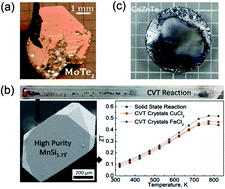
According to the above equation, X2, MCl5 and Cl2 are all relevant molecular species present in the reaction atmosphere; therefore the pressure balance is controlled by the relative content of X2, MCl5 and Cl2. In this case, it is very critical to choose an appropriate proportion for the starting mixture. After evaporating between 2 days and 1 week, the single crystals are either isolated or in small aggregates or even as thick crystal layers, which are nucleated and grown on the quartz wall of the ampules in the cold region. The average sizes of the crystals range from a few to fifty square millimeters. Fig. 1a shows a crystal of MoTe2 grown at Thot = 850 °C and a low chlorine content (Mo[thin space (1/6-em)]:[thin space (1/6-em)]MoCl5 = 10). It is shown that nucleation is well-controlled by the chlorine partial pressure, as crystal growth is more determined by the chalcogen partial pressure. In addition, the sublimation temperature depends mainly on X, and the initial M[thin space (1/6-em)]:[thin space (1/6-em)]MCl5 ratio is the most critical influential factor on crystal growth. By using the similar reaction procedure, high-purity single crystals of higher manganese silicide (HMS) were also prepared by using a modified vapor transport approach.8 It is found to be effective to generating a large quantity of high-quality crystals by using transition metal halides CuCl2 or FeCl2 as additives. Take CuCl2 as an example, the net reaction at the source can be described as the following reaction equation:8

 
image file: c5ra13349a-t2.tif(2)


image file: c5ra13349a-f1.tif
Fig. 1 (a) Image of MoTe2 single crystal grown at Thot = 850 °C from a low chlorine content, Mo[thin space (1/6-em)]:[thin space (1/6-em)]MoCl5 = 10. (b) Photograph of the sealed fused silica tube for HMS crystal growth using CuCl2 as the transport agent, showing the starting material in the source zone and product at the growth zone; SEM image of the HMS single crystal product with detail of well-faceted planes obtained using FeCl2 as transport agent; thermoelectric efficiency of HMS made by SSR and CVT. An enhancement in hole mobility produces a higher electrical conductivity in the CVT samples. (c) Typical CZT crystal comprises a single grain in the central region.

In this case, the starting source was synthesized using a solid state reaction by reacting high purity Si and Mn at a ratio of 1.73[thin space (1/6-em)]:[thin space (1/6-em)]1. The vaporized CuCl2 serves as the transport agent and no Cl2 was generated in this reaction, which differs from eqn (1). If choosing MnCl2 directly as a transport agent, the chemical reaction was not as effective, resulting in low yield and very small HMS crystals. That is to say, the substitution of Mn by other kind of more active transition metal is vitally important in such kind of VS process. As shown in Fig. 1b, the HMS crystals exhibit improved maximum thermoelectric efficiency up to 0.52 ± 0.08 at 750 K, owing to their higher purity as well as enhanced hole mobility in comparison to the samples synthesized using traditional solid-state techniques. In addition, Steiner et al. also successfully synthesized β-Mg1−xNixMoO4 crystals by using Mg1−xNixMoO4 powder as source and platinum chloride as additive in a two-zone furnace,9 where the Mg1−xNixMoO4 and platinum chloride powders were placed in an evacuated silica ampoule. To avoid contact of the decomposed platinum with Mg1−xNixMoO4 crystals, the platinum chloride was previously introduced in a small one side closed quartz tube. Similar to the above experimental procedures, CuS had also been prepared by vapor transport reaction;10 the difference is that the source is directly transported towards the cold zone of the ampoule to form single crystals by the transporting agent iodine.

Multi-tube physical vapor transport (MTPVT) is actually another way of vapor transport reaction, so called because the source materials are evaporated independently by the system geometry. Upon using the MTPVT, (Cd, Zn)Te (CZT) single crystals had been successfully prepared.11,12 Before growing CZT, an initial CdTe nucleation layer of a few millimeters grown on a GaAs (111) substrate is acted as seeding layer, which is put in the low temperature region. Then, the CZT single crystals can grow by evaporating the high purity cadmium telluride and zinc telluride source materials at a comparatively low temperature. Fig. 1c shows a typical CZT crystal comprises a single grain in the central region.11 The crystal is approximately 50 mm in diameter and 11 mm thick. A planar device (Au/CdZnTe/Au) based on this material shows electron mobility lifetime of 4.07 × 10⁻³ cm2 V−1. The CZT crystal fabricated according to the same procedure by Andreas et al.12 show a high resistivity up to 2.3 × 10¹¹ Ω cm, indicating a promising candidate as an X-ray detector.

Aluminum nitride (AlN) is reported as one of the most important versatile semiconductors with a direct wide band gap of 6.2 eV and excellent transparency in the ultra-violet (UV) range, thus promising for applications like light emitting devices and UV optoelectronic devices. In a vertical semi-open crucible where the source zone is on the lower and the crystal growth zone is on the upper, single crystal AlN can be deposited on a perforated sheet which acts as nucleation area inside the crucible above the source material, and polycrystalline AlN layer is typically grown on the crucible lid.13

2.2. Organic single crystals

The advantages of organic crystals such as high thermal stability, high carrier mobility and high ordered structure make them great candidates for use in optoelectronic devices. Several organic crystals of anthracene (Ac), tetracene (Tc), pentacene (Pc) and 2,5-diphenyl-1,4-distyryl benzene with two trans double bonds (DPDSB) had been prepared by vapor transport reactions with sublimation temperatures of 170 °C, 200 °C, 300 °C and 220 °C in the source zone, respectively.14 The sublimated source materials were transported with a carrier gas (Ar, 99.999%). After 2–3 growth days, all the products forming slice-like shapes, smooth surfaces and larger sizes, hang in the growth tube with increasing sizes along the decreasing temperature gradient. Based on the crystal growth thermodynamic characteristics, Tc doped Ac crystals had also been prepared corresponding to the low temperature and high temperature growth conditions, respectively. It is proved that doping Tc into the Ac crystal can effectively increase the luminescence efficiency, which is ∼40% and ∼74% for sky-blue emission and green emission, respectively. Fig. 2a shows the emission spectra of Tc doped Ac crystals prepared at different temperatures, which indicates the green emission mainly comes from Tc molecules and the sky-blue emission comes from both Ac and Tc molecules. Thus vapor transport reaction paves a new way for design and preparation of color-tunable and high-luminescence efficiency organic crystals.
image file: c5ra13349a-f2.tif
Fig. 2 (a) The emission spectra of Tc doped Ac crystals prepared at the low temperature (70 °C) and the high temperature (100 °C). Insets are the optical photographs of Ac doped Tc crystals corresponding to the emission spectra. (b) Typical configuration of a PDA single crystal grown by the vapor transport method and images of the PDA single crystal before (c) and after (d) the application of mechanical stress.

Polydiacetylenes (PDA) in single crystal form is one type of functional organic material, which exhibit a variety of interesting physical properties that can be applied in electronic devices. PDA grown by the vapor transport reaction was reported by Sadaharu et al., the effect of solid-state polymerization on the crystal morphology was well studied.15 Crystal configuration of polymer material is affected by the formation of polymeric chains, which induces anisotropic changes in crystallographic orientations. Fig. 2b shows a typical platelet-like morphology of a PDA single crystal with a pair of large parallelogram (010) planes and four narrow lateral planes (100), ([1 with combining macron]00), (001), and (00[1 with combining macron]). Fig. 2c and d is the photograph before and after a mechanical stress is applied to the PDA single crystal, respectively. This kind of cleavage characteristic of this type of PDA single crystal, indicates that most of the polymeric backbone chains were constructed along the [001] direction.

3. Deposition of thin films

3.1. Solar cell thin films

SnS is a natively p-type semiconductor known to have a suitable bandgap (1.1–1.3 eV) and high absorption coefficient, which is a promising candidate for single-junction solar cells. Vapor transport method supplies a low-cost and efficient way for depositing SnS thin films. Generally, the synthesis process could be briefly described as evaporating tin(II) sulfide powder in a horizontal tube furnace with the substrate downstream at a proper temperature. The thickness of the film can be controlled by the deposition time. The synthesis product is also strictly connected with the distance from the substrate to the source. As reported by Wangperawong et al.,16 polycrystalline thin films in the sequence of SnS, Sn2S3, and SnS2 were deposited further downstream onto glass substrates. In this case, the deposition temperature is decreased further downstream, but the vapor pressure is lowest for SnS and highest for SnS2. In addition, all the thin films deposited on glass substrates exhibit various orientations, while the SnS thin films deposited on NaCl (100) substrate is preferentially oriented with (010) planes with sheet-like stacking morphology. Fig. 3a is the cross-sectional SEM image of a 600 nm thick SnS film on NaCl. According to the refractive index and absorption coefficient studies, the bandgap of the heteroepitaxially deposited SnS thin films are 1.0 eV (indirect) and 2.3 eV (direct), respectively. Recently, the SnS absorber layer in solar cell device consisting of glass/FTO/SnS/CdS/ZnO/ITO was also produced by vapor transport method (Fig. 3b and c), as reported by Wangperawong et al.,17 the front- and back-side power conversion efficiency is 1.2% and 0.2% (Fig. 3d), respectively, due to the fact that ITO and FTO are both transparent conductors.
image file: c5ra13349a-f3.tif
Fig. 3 (a) Cross-sectional SEM of SnS (010) thin film grown epitaxially on NaCl (100). (b) Surface SEM image of SnS grown on glass/FTO substrate. (c) Cross-sectional SEM image of glass/FTO/SnS/CdS/ZnO/ITO bifacial solar cell. (d) Current–voltage data of glass/FTO/SnS/CdS/ZnO/ITO solar cell device in the dark (dotted line), and under frontside (solid line) and backside (dashed line) AM 1.5G illumination.

Cu2ZnSnS4 (CZTS) thin-film solar cell consists of earth-abundant and environment-friendly elements and thus is promising candidate for real device applications. As reported by Toyama et al.,18 vapor transport method can also serve as a great way for post annealing on CZTS films, which results in improved power conversion efficiency (6.9%) as absorber layer in solar cell. The rf magnetron sputtering deposited CZTS films were annealed at 550 °C for 3 h by vapor transport method using a mixture of H2S and N2 as carrier gases with a ratio of 5/95, meanwhile, SnS2 powder was introduced as the Sn vapor source in the upstream furnace and the CZTS films were placed in the downstream furnace. The grain size of CZTS films after vapor transport method annealing is significantly increased (Fig. 4). The chemical compositions of the CZTS film show a slight change in the Sn fraction after annealing, while the composition becomes Cu-deficient and Zn-rich, which is beneficial for increasing the power conversion efficiency. As summarized in Table 1, all of the CZTS thin films prepared by the different method exhibit direct band gap energy about 1.5 eV which is optimum value for being used as an absorber layer in solar cells, however, the highest power conversion efficiency is obtained in the thin film prepared by using the vapor transport method.


image file: c5ra13349a-f4.tif
Fig. 4 FESEM images of the CZTS thin film surfaces: (a) precursors, and annealed (b) without or (c) with vapor transport method.
Table 1 Summary of the values of grain size, optical band gap, and the conversion efficiency of CZTS thin film solar cell prepared by different method
Preparation method Grain size Band gap Power conversion efficiency Ref.
Vapor transport 23 nm 1.5 eV 6.9% 18
Solvothermal 11–12 nm 1.37–1.54 eV 0.10–0.16% 83
Screen printing 50–200 nm 1.49 eV 0.49% 84
Pulsed Laser deposition 100 nm 1.5 eV 1.74% 85
Electrochemical deposition 2 μm 1.51 eV 2.3% 86
Electrochemical deposition 100 nm 1.64 eV 5.5% 87
Sol–gel 300 nm 1.5 ± 0.02 eV 3.02% 88


Bismuth sulfide (Bi2S3) is another alternative inorganic material used as absorber layers in thin film solar cells.19,20 The effects of the deposition temperature on the structural and electrical properties of polycrystalline (Bi2S3) thin films were investigated by Haaf et al.21 During the deposition of Bi2S3, indium tin oxide (ITO) substrates were kept at various temperatures between 80 °C and 290 °C above the source. As the deposition temperature increases, a transition from needle-liked particles in (hk0)-orientation that parallel to the surface of the substrate to block-like grains with a preferred direction out of the surface plane could be identified. In addition, an increase of the conductivity from 2 × 10⁻⁷ to (2.5–8.5) × 10−3 Ω−1 cm−1 was also obtained.

3.2. Transition metal dichalcogenide monolayers

Transition metal dichalcogenides (TMD) have succeeded in the growth of monolayer thin films22–24 and have recently become a new focus of attention due to their significant promise for applications in electronics and optoelectronics. WSe2 is one kind of TMD family and has been successfully grown in large volume by using chemical vapor deposition techniques.25,26 Alternatively, the vapor transport method have been recently demonstrated to synthesize WSe2 monolayers with high crystal quality and low concentration of defects.27 The growth method is locating the WSe2 powder in a crucible placed in the hot zone of a horizontal tube furnace, and a SiO2 substrate is placed at a distance of ∼5 cm downstream from the source at a much cooler temperature (750–850 °C). WSe2 monolayers of up to 30 μm edge length could be grown by this method. Fig. 5a shows an optical image of the WSe2 monolayers grown on SiO2 substrate, where a variety of morphologies are present corresponding to different regions of the substrate as shown in the magnified images in Fig. 6b–d. It can also be seen from the higher temperature (“i”) to the lower temperature region (“iii”) that the density of the WSe2 monolayers becomes lower, suggesting a significantly higher nucleation density in the higher temperature region. The atomic force microscope image reveals that the surface of the WSe2 monolayer is very uniform and flat, and the average thickness of the triangle product is nearly 0.77 nm. The monolayers grown using this method demonstrated well resolved and electrically tunable excitonic features due to the high crystal quality.
image file: c5ra13349a-f5.tif
Fig. 5 (a) Optical image of WSe2 grown on SiO2 substrate. (b–d) show the optical microscope image of WSe2 monolayers from region “i”, “ii” and “iii”, respectively, of substrate in (a). (e) AFM image of WSe2 monolayer with inset showing height profile averaged from three different 4 μm sections across the edge of the triangle sheet.

image file: c5ra13349a-f6.tif
Fig. 6 Typical SEM images of (a) Te, (b) Ge, (c) Sb-doped Si and (d) Mn-doped Ge nanowires. Inset in (d) is an individual nanowire with diameter of 80 nm.

3.3. Close space vapor transport

A modified vapor transport method, closed spaced vapor transport technique (CSVT), are reported to produce low cost, large area and high quality thin films.28,29 The ternary compounds Cu–III–VI2 family had been extensively studied due to their high potential for device applications in solar cells, photodiodes and nonlinear optic technologies. However, there are few reports on CuGaTe2 (CGT). Abounachit et al.28 had deposited CGT films by CSVT and reported that the source temperature and the pressure of transport agent iodine could influence on the product quality. Most importantly, adding an amount of pure copper to the starting materials can improve the quality of the CGT film and reduce the operating temperature. As known to all, gallium nitride (GaN) has been considered as a promising material due to its wide band gap (3.4 eV at 300 K), good stability at high temperature, and excellent thermal conductivity. The CSVT had been proved as a low-cost approach to grow high quality GaN thin film with very fast growth rate.29 The growth experiments were performed in two screwed graphite crucibles with lower part containing the GaN source powder and the substrate in vacuum condition, using infrared lamp as heating power. The structure of the GaN depends extensively on the type of the substrate. The samples grown on silicon and sapphire substrates are polycrystalline, whereas the samples grown on fused silica result in amorphous GaN. Anyway, vapor transport method is proved to be a high yield technique with simple equipment set-up to obtain suitable quality polycrystalline GaN thin films.

4. Synthesis of one dimensional nanostructure

4.1. Growth mechanisms on one-dimensional nanostructures

Based on the growth of one-dimensional nanostructures, three important growth mechanisms had been proposed and proved in each experiment by researchers, including vapor–liquid–solid (VLS), vapor–solid–solid (VSS) and vapor–solid (VS) growth processes. The VLS process, known as metal catalytic growth, utilizes a catalytic preferential deposition site for which material in the vapor phase can be absorbed.30–32 Therefore, a metal catalysis is essentially to form a liquid alloy droplet as seed particles for nanowire growth in this process. A nanosize catalyst, Au particle in general, can form a liquid metal droplet on the substrate even though the evaporation temperature is far below its melting point. At the same time, the liquid catalyst droplet can continually absorb the vapor phase precursor into the drop and exist as eutectic mixture. Upon the liquid alloy droplet becomes supersaturated, the precursor phase precipitates at the bottom of the drop. The continuation of this process leads to the growth of a nanowire with the catalyst sitting atop of the nanowire. Using this growth mechanism, nanowires can be synthesized with different diameters by flexibly controlling the catalyst diameter, and the nanowire length can be extended by increasing the growth time. As reported by Renard et al.,33 Germanium nanowires were grown on germanium (111) substrate via the VLS growth mechanism, using gold as catalyst. The results showed that the nanowire length also depends on the diameter of the catalyst particle, the smaller the nanowire radius, the slower the nanowires grow. Thus the diameter of the catalyst particle could also determine the rate of absorption–precipitation process.

It has been realized that VLS process can occur in the case where the catalyst particle is solid with sharp facets yielding the so-called vapor–solid–solid (VSS) growth. Recently, it has been reported by Zou et al.34 both the Bi2Se3 nanoribbons and nanowires are governed by the VSS growth mechanism, since the post-growth catalysts for both structures are faceted, suggesting that the catalysts are in solid form during the nanostructure growth. Furthermore, the Bi and Se atoms in vapor cannot form a liquid alloy with Au particles due to the fact that the eutectic reaction cannot happen in the corresponding growth environment. On these bases, the metal catalyst exists in a particle form rather than the liquid catalyst droplet during the entire process of the nanostructure growth. Previously, Kodambaka et al. studied VLS and VSS growth of germanium nanowires in situ by transmission electron microscopy.35 It was found that VSS growth was 10–100 times slower than VLS growth, which could be attributed to lower surface reactivity and/or slower diffusion of Ge across the solid catalyst particle. Generally, the VSS growth process could be determined by the following rate-limiting steps,36 i.e., precursor vapor phase transport to the catalyst, surface reaction at the catalyst surface, and solid phase diffusion of the precursor across the catalyst particle to the catalyst/nanowire interface. Therefore, the kinetic processes at the two interfaces, gas/catalyst and catalyst/nanowire, are understood to be of crucial importance in VSS growth process.

In contrast to the VLS and VSS growth, the nanowires can be generated directly from the vapor phase without metal catalyst, and this process is often named as vapor–solid (VS) growth.37,38 During evaporation, the starting source first evaporates and decomposes into vapor phase through pyrolysis process, gas phase reaction or chemical reduction. Then when the vapor phase becomes supersaturated, it can concentrate on the substrate in the low-temperature area to form liquid droplets that act as catalysts for nanowire growth. At the droplet–substrate interface, a microdefect and a preferred orientation are selected as nucleation center and growth direction for nanowire growth.

4.2. Nanowires

Nanowires are extensively studied by many groups due to their novel physical, chemical, optical, mechanical and biological properties. In the past five years, nanowires consisting of elementary substances, oxides, chalcogenides, phosphides, nitrides, ternary oxides and heterostructures with different valence states and different crystal structures, including Bi2Se3,34 Te,39 Ge,40 Sb-doped Si,41 Mn-doped Ge,42 VO2,43–55 ZnO,56–59 SnO2,60,61 NbO2,62 Ga2O3,63 CdO,64,65 PbS,66 SnTe,67 PbTe,68,69 Ag2Te,70 ZnTe,71 AlN,72 InN,73 Zn3P2,74 Zn2GeO4 (ref. 75) and ZnGa2O4 (ref. 76) have been successfully synthesized by vapor transport method. These nanowires are of great scientifically and technologically significance due to their potential applications in various areas, such as optical, electrical, photovoltaic, thermoelectrical and sensing devices. Some of these materials are narrow bandgap semiconductors such as Te and Ge,39,40 while some have a wide band gap such as Zn2GeO4 and ZnGa2O4.75,76 During the experiments, the choices of experiment parameters vary with the types of nanowires. For example, the temperature was held at 300 °C for the duration of the Te nanowire growth,39 however, the source should be heated to 1850 °C during the AlN nanowire growth.72 This is not an exhaustive literature review, but rather gives some representative works as following.
4.2.1 Elementary substance nanowires. Fig. 6 shows the scanning electron microscope (SEM) images of the single crystalline Te, Ge, Sb-doped Si and Mn-doped Ge nanowires that are grown on the 200 nm thick silicon dioxide on Si (111) wafers or Au coated Si substrates with different coating layer thicknesses.39–42 High resolution TEM analysis confirmed the growth directions of the above single crystalline nanowires are [001], [111], [111] and [110], respectively.

Elemental Te is a narrow bandgap p-type semiconducting metalloid, which has shown great potential applications due to its multifunctional characteristics, including photoconductive, piezoresistive and nonlinear optical properties. The size of the as-grown Te nanowires varies from 30 nm to >6 μm in diameter and from few hundreds nanometers to >30 μm in length (Fig. 6a). The average nanowire diameter and length are tailorable, which bases on the evaporation temperature as well as deposition time in the VS growth regime. The average nanowire length increases with increasing evaporation temperature, and a higher temperature can improve the nanowire nucleation rate effectively, resulting in a higher nanowire density. Combination of the initial higher temperature nucleation step and the lower temperature growth step, called two-step temperature growth,39 produces high density nanowires with smaller diameters. Such growth demonstrates a practical approach to synthesizing high-quality tellurium nanowires of various sizes and provides a method to growing two-dimensional mesh-like structures through controlled nucleation and growth dynamics.

Germanium in nanowire form has been extensively used in various nanoelectronic systems such as field effect transistors, photoresistors and photodetectors due to its semiconductive nature with a bandgap of 0.67 eV. Basing on the vapor transport method, Aksoy et al. reported on the synthesis of Ge nanowires using Ge, GeO2 + C and GeI4 + Ge powder mixture as precursors.40 The growth of Ge nanowires are suggested following VLS mechanism because of the hemispherical Au catalyst at the tip of the nanowire. The influences of various temperatures and pressures on the synthesized Ge nanowires with different starting precursors are investigated. It is confirmed that increase in both pressure and temperature can significantly increase the diameter of the nanowires independent of precursor type. A relative higher temperature leads to the diffusion of Ge into larger Au particles allowing an easier growth of Ge nanowires with larger diameters. Furthermore, increase in system pressure decreases the Ge vapor saturation level, leading to increase the diameter of Ge nanowires to reduce the surface energy. As shown in Fig. 6b, the optimum temperature and pressure for the synthesis of Ge nanowires using GeO2 + C powder mixture are found to be 850 °C and 200 mbar, respectively. Micron-sized spherical particles grow at high temperature and thin film growth initiates accordingly above 100 mbar when using GeI4 + Ge powder mixture as precursor.

Benefited from the compatibility with present integrated circuit technology, semiconducting Si nanowires are promising for applications in nanoscale electronics. Especially, vapor transport method shows great ability to modify the Si nanowires to be either n- or p-type by doping, thus extending greatly the application area. Nukala et al. explored an expensive-effective method for synthesis of n-type Sb-doped Si nanowires with lengths of 30–40 μm and diameters of 40–100 nm (Fig. 6c) by using SiCl4 as source and pure Sb as dopant.41 For the purpose of increasing the doping level of Sb into the Si nanowires, the as-grown Si nanowires are instantaneously annealed in Sb vapor in Ar atmosphere. The concentration of Sb in the Si nanowire is found to be highly dependent on the evaporation temperature. After doping with Sb, the nanowires exhibit n-type behavior in comparison to the p-type behavior of as-grown Si nanowires, accompanying with significantly improved electrical transport character.

The investigations of diluted magnetic semiconductors (DMSs) on transition metal doped semiconductor thin films cannot doubtlessly eliminate the influence from magnetic impurity phases. However, the vapor transport method can be exploited for synthesizing nanowires that are thermodynamically stable, single-crystalline and defect-free. Previously, a study on Mn-doped Ge nanowires grown on the silicon substrate by VLS mechanism using Au as catalyst has been reported.42 The synthesis procedure of this material is fairly special that the GeCl4 as Ge source is introduced into the reaction chamber using H2 carrier gas that is bubbled through a liquid source. In contract to the Ge nanowire grown along [111] direction,39 the growth direction of the Mn-doped Ge nanowire is [110]. Fig. 6d shows a SEM image of typical Mn-doped Ge nanowires with diameter and length from 50 to 100 nm and tens of micrometers, respectively. These nanowires possess room-temperature ferromagnetism ascribed to the local magnetic moment with the 3d5 electronic configuration of Mn2+ ion. Electrical characterization also indicates better p-type gating response and higher hole mobilities on these nanowires. The result implies that the transition metal doped semiconductor nanowires opens the possibility of determining the intrinsic magnetism under fully relaxed states, and it would helpful for developing DMSs based spintronic devices.

4.2.2 Oxides. As an ideal candidate for applications in electrical and optical switching devices, VO2 nanowire, belongs to oxide family, has been the most widely investigated material due to the unique metal-to-insulator transition (MIT) phenomenon, accompanying with a reversible structural transition from a high-temperature tetragonal (T) phase to a low-temperature monoclinic (M) phase at about 340 K.43–46 Almost two kinds of VO2 nanowires are prepared by the vapor transport method, one is the clamped VO2 nanowire which is generally laying on the substrate, thus generating a latent strain in the body due to the lattice mismatch and different thermal expansion coefficients between the wire and the substrate;47–51 the other is freestanding grown VO2 nanowires,52–55 which are beneficial for studying the MIT mechanism by fully eliminate the substrate-imposed strain effect. All of these VO2 nanowires tend to grow along the monoclinic [100] direction as deposited on various substrates, such as rutile TiO2, GaN, SiN, sapphire, SiO2 coated Si, quartz and rough quartz,47–55 accompanying with a rectangular cross section and two crystallographically equivalent side facets (011) and (01[1 with combining macron]). The growth mechanism of VO2 nanowires by vapor transport method matches well with the VS mechanism, where vanadium oxides undergoes evaporation and/or decomposition to various oxidation state due to the fact that vanadium oxides can exist in a wide range of stoichiometries. Then the vapor phase is carried downstream by the carrier gas, and the stable VO2 phase can nucleate from the vapor phase and deposit onto the substrates.

As shown in Fig. 7, the VO2 nanowires are prepared on a sapphire substrate with its (011) and (01[1 with combining macron]) surfaces parallel to the nanowire axis, and from the cross-sectional TEM image one can see two side facets are buried into the sapphire substrate. According to the atomic structure of the nanowire–substrate interface (Fig. 7b), the tenfold d-spacing of (010) VO2 (T) is about 4.554 nm, which matches fairly well with the value of the nineteen times (110) Al2O3 planes. Thus a compressive strain should be formed in the nanowire; furthermore, the lattice shrinkage from the high-temperature T phase to the low-temperature M phase could further induce a compressive strain in the VO2 nanowire. Fig. 8a and b shows the other kind of VO2 nanowire horizontally grown on the SiO2 substrate with one side facet stick on substrate surface. The nanowires are around several hundred micrometers long with diameters in the range of 200–800 nm. The starting material for the synthesis of these kinds of VO2 nanowires is V2O5 powders, which is loaded into the middle of a quartz tube in a horizontal furnace system with an argon gas protection at 800 °C and 8 Torr for 3 h. TEM analysis indicates that the VO2 nanowires with the [1[2 with combining macron]2] zone axis are grown along the [100] direction, which is vertical to the ([2 with combining macron]01) plane. The lattice fringes of adjacent (011) planes are about 2.8 Å. Fig. 8f shows the fabrication process for making a single microwire VO2 photodetector, and the optical microscope image in Fig. 8g reveals that a single VO2 microwire with a length of ∼130 μm is successfully bonded by the silver electrodes SiO2/p-Si substrate. It was demonstrated that the responsivity of this single VO2 nanowire photodetector is 6 and 4 orders higher than that of graphene (or MoS2) and GaS based devices on SiO2/Si, due to the high efficient hole-trapping effect.46


image file: c5ra13349a-f7.tif
Fig. 7 (a) A cross-sectional TEM image of a single VO2 nanowire grown on a sapphire substrate with its (011) and (01[1 with combining macron]) surfaces parallel to the nanowire axis. (b) An HRTEM image showing the interface structure and its corresponding FFT patterns (inset) to confirm the orientation relationship between the nanowire and the substrate.

image file: c5ra13349a-f8.tif
Fig. 8 (a) FESEM images of VO2 nanowires, (b) cross-sectional image of one typical VO2 nanowire with diameter 200−800 nm. (c) TEM image of an individual VO2 nanowire. (d) SAD pattern showing the side facet bound by (011) and ([2 with combining macron]01). (e) HRTEM image showing the nanowires' growth direction of the [100] axis. (f) The fabrication process of an individual VO2 microwire photodetector. (g) A digital optical microscope image of a VO2 microwire.

For the synthesis of freestanding VO2 nanowires, V2O5 powder source and unpolished quartz substrate are strongly suggested by researchers.50,51 Fig. 9a shows the SEM image taken from the side view, further indicating that the nanowires are grown free-standing from the unpolished quartz substrate. Two influence factors are considered to be crucial importance for prompting the VO2 nanowires growth. First, under the same reaction conditions, V2O5 can provide much higher vapor pressure due to its much lower melting point of 690 °C than that of VO2 (1967 °C). Therefore, more vapor molecules can be adsorbed and diffuse to the growth front of the nanowire, resulting in a faster growth. Secondly, the unpolished quartz substrate provides random nucleation centers and growth directions for the nanowire growth. At the beginning, the nanowire grows following the surface roughness of the substrate as lying on a small flat. Later, the growth front of the nanowire extends out the plane and becomes free-standing (Fig. 9b). In addition, reactant molecules would be adsorbed to the free-standing nanowire easily when it is imposed into the vapor phase. These growth characteristic explain the random orientation of the as-grown nanowires felicitously.


image file: c5ra13349a-f9.tif
Fig. 9 (a) Optical image taken from the side view showing free standing VO2 nanowires. (b) Proposed growth mechanism of free-standing VO2 MNWs on rough quartz substrates.

ZnO is a unique material with a wide band gap of 3.37 eV and a large exciton binding energy of 60 meV at room temperature. The ZnO nanowire has been one of the most widely investigated inorganic nanomaterials due to its expansive applications in electronic, optoelectronic, photovoltaic and sensing devices.56–59 Zn powder and oxygen gas flow or ZnO and graphite powder mixture are commonly used as the starting sources for the synthesis of ZnO nanowires.

It is generally believed that the vertical growths of ZnO nanowires are realized on lattice-matched substrates such as ZnO or sapphire. However, Ngo-Duc et al. demonstrated an easy way for vertical ZnO nanowire growth on metal FeCrAl substrate.56 The FeCrAl substrate is annealed in a gas mixture comprising a 1[thin space (1/6-em)]:[thin space (1/6-em)]2 ratio of H2[thin space (1/6-em)]:[thin space (1/6-em)]Ar for 30 min at 450 °C, then the FeCrAl substrate is placed on a boat that contains the Zn powder precursor and transferred into the quartz tube furnace. The pre-annealing prior to growth appears to preferentially result in a sapphire-like surface layer on the FeCrAl substrate which then results in vertical nanowire growth as on sapphire. The ZnO nanowires shown in Fig. 10a are mostly vertically oriented on the FeCrAl metal substrate with lengths of ∼10 μm and 200 nm in diameters. Fig. 10b shows the jagged-shaped end of the nanowires and Fig. 10c shows a high resolution TEM image at the nanowire tip. The nanowire has a (0002) lattice spacing of 0.26 nm which is consistent with ZnO growth along the preferred [0001] direction. One important influential factor on the growth of ZnO nanowire basing on the vapor transport reaction is the distance between the source and the substrate. Vega et al. investigated ZnO nanowires grown on Au-nanocluster-seeded amorphous SiO2 films,57 which are covered by a rough ZnO seed layer whose formation is catalyzed by the Au clusters during nanowire growth. As such, the nanowires are oriented perpendicular to substrates and their mean size decreases significantly with increasing the distance between source and substrate. This method shows an interesting approach to produce ZnO nanowires with controllable diameters and lengths. Quartz substrate is another well used material for the growth of ZnO nanowires, Hosseini et al. found that the nanowires grown on the quartz substrates possess stronger c-axis orientation compared to those grown on the alumina.59 As shown in Fig. 10d, the response transients of the sensors to 5000 ppm acetone at optimum operating temperature reveal the higher response and shorter recovery time for quartz samples compared to alumina ones. The explanation to this phenomenon is that the aligned ZnO nanowires on the quartz substrate could make gas quickly diffuse in or out, consequently prompt the contact reaction efficiency between the nanowire and the gas resulting in higher response and quick recovery.


image file: c5ra13349a-f10.tif
Fig. 10 (a) Vertically aligned ZnO nanowires grown on FeCrAl metal alloy substrate. (b) TEM image of ZnO nanowires at the tip section and (c) high resolution image TEM of the nanowire base showing a (0002) lattice spacing of 0.26 nm. The growth direction is also noted by the arrow. (d) The response transient curves of quartz sensor under exposure of different acetone concentrations (solid curve) and alumina sensor under exposure of 5000 ppm acetone vapor (dashed curve).
4.2.3 Sulfides, selenides, and tellurides. Nanowires consisting of sulfides, selenides, and tellurides are in the focus of numerous researches. PbS with narrow band gap is an excellent infrared absorber and can be used in a multijunction solar cell to collect the infrared light, especially in nanowire form providing much more efficient transport channels for photocarrier extraction. As reported by Graham et al.,66 a single crystalline PbS nanowires are synthesized via the VLS mechanism following a slightly modified vapor transport method. Briefly, PbCl2 powder is placed at the center of a horizontal and S powder is placed upstream just outside the mouth of the furnace. At the peak temperature, H2 is used to reduce PbCl2 to Pb catalytic nanoparticles, which react with S vapor immediately to grow PbS nanowires on Si (100) substrate downstream. The resulting nanowires range from 50 to 125 nm in diameters and are up to tens of micrometers in lengths. The nanowires show p-type characteristic with hole mobilities up to 49 cm2 V−1 s−1, accompanying with photoresponse time faster than 14 μs.

Bi2Se3 and SnTe at the nanoscale have attracted great interest since its theoretical predication as topological crystalline insulator for future electronic and spintronic applications. High-quality single crystalline Bi2Se3 nanowires via gold-catalyst VSS growth mechanism by vapor transport reaction have been successfully synthesized.34 It is very essential to mention that the growth of Bi2Se3 in nanowire and nanobelt, as well as nanowire–nanobelt junction structures can be prepared under the same synthesis condition.34 The structure analyses reveal that the interfaces between catalyst and these nanostructures are significant different. They are always {0001} interfaces for the case of nanowires and nanowire–nanobelt junctions, while the nanobelts and their catalysts always have multifaceted interfaces. Therefore, the geometrical shape of the gold catalyst is crucial for the VSS growth mechanism. By contrast, the SnTe nanowires grown on the Au-coated Si substrate through the VLS mechanism were uniform and dense, with about 10 μm in length and 59 nm in diameter.67 The quantum transport measurement on these single crystalline and pure SnTe nanowires show for the first time well distinguished Aharonov–Bohm interference and Shubnikov–de Haas oscillations.67 Thus the vapor transport method is benefit for future exploration of new topological crystalline insulator materials.

PbTe has been the subject of particular attention due to its high thermoelectric efficiency. Lee et al. demonstrated that the thermoelectric performance of individual PbTe nanowires grown from the vapor transport method was much higher than that of bulk PbTe;68 besides, the PbTe nanowires synthesized through the gold-assisted VLS mechanism are high-quality and single-crystalline, thus can be used to fabricate field-effect transistors for studying intrinsic thermoelectric transport properties.68,69 Furthermore, the Seebeck coefficient and thermal conductivity of the PbTe nanowires were found to be size dependent.68

In addition to Au commonly serving as catalyst in nanowire growth, it is proved that Bi works well enough as Au in catalyst-assisted ZnTe nanowire growth. Moon et al. had prepared ZnTe nanowires using ZnTe powder as source placed in the center zone and Bi powder as catalyst placed at 13.5 cm upstream from the center, and Si substrates that are cleaned and hydrogen-terminated by diluted HF are placed at 14.5–18 cm downstream from center.71 Straight and single-crystalline nanowires are grown at relatively low substrate temperatures (410–360 °C). Fig. 11a shows the side-view FESEM images of as-grown ZnTe nanowires with diameter 200–400 nm and ranging from ∼50 to ∼200 μm in length, which is the longest nanowire reported so far grown by the vapor transport method. From Fig. 11b, a nanowire with a catalyst on its top can be clearly observable. The TEM analysis confirms the ZnTe nanowires catalyzed by Bi is single-crystalline with [111] growth direction (Fig. 11c and d). In addition, this kind of ZnTe nanowire shows interesting color tuning from green to red in photoluminescence measurement as varying the excitation laser position from the tip toward the bottom of the nanowire.


image file: c5ra13349a-f11.tif
Fig. 11 (a) Side-view FESEM image of as-grown ZnTe nanowires. (b) FESEM image of a single nanowire transferred to Si substrate. (c) Low-magnification TEM. (d) SAED pattern observed through [110] zone axis.
4.2.4 Ternary oxides. The vapor transport method has also been explored to synthesis more complicated compound, such as ternary oxides Zn2GeO4 (ref. 75) and ZnGa2O4.76 Taking Zn2GeO4 nanowire as an example, the growth process can be explained by Au directed VLS mechanism due to the simultaneous adsorption and precipitation of Zn and Ge species at the interface of supersaturated Au and substrate.75 During the experiment, besides ZnO and Ge, carbon powder is also added to the source region. On the one hand, carbon powder serves as the reduction agent to decompose ZnO into Zn. On the other hand, carbon also serves to maintain the Ge vapor pressure during the nanowire growth. The optimum molar ratio of ZnO/Ge is proved to be 2/1 for synthesizing stoichiometric Zn2GeO4 nanowires without formation of additional ZnO or Ge phases. Au is shown to be essential to produce high quality Zn2GeO4 nanowires due to the fact that only polycrystalline films and microparticles can be found on the substrate without Au catalyst. This also implies that the VS mechanism is not recommend for the optimum synthesis of Zn2GeO4 nanowire basing on the same conditions. A majority of the as-synthesized Zn2GeO4 nanowires are straight with growth direction along [110], but ∼5% of them are branched structures. As schematically shown in Fig. 12a, the straight Zn2GeO4 nanowires are grown via common VLS mechanism, and the model in Fig. 12b is well used to explain the growth of branched Zn2GeO4 nanowires. It indicates that the Au droplets may attach on some of the tilted nanowire body during growth, and the attached Au nanoparticles served as catalysts for branch nanowires growth.
image file: c5ra13349a-f12.tif
Fig. 12 Growth models for the (a) straight and (b) branched Zn2GeO4 nanowires.

4.3. Nanobelts and nanorods

Generally, nanobelt has relative smaller aspect ratio than that of nanowire, while nanorod looks almost like nanowire but exhibiting relative larger size. As reported by Cabán-Acevedo et al.,78 FeS2 nanobelts and nanorods could be synthesized at the same reaction condition independent of the precursor spices. Thus more detailed study must be done for deep understanding the growth mechanisms of nanobelts and nanorods.

Wei et al.77 synthesized Bi2Te3 nanobelts by gold-mediated VLS growth with average width of 200 nm and average length of 10 μm. It is observed that there are only few tiny Bi2Te3 particles and blocks and no nanobelt appears on the quartz substrate without Au colloid as catalyst. The results clearly indicate that catalyst particles are essential for the growth of nanobelt. This is also proved by the synthesis of Mn-doped ZnS nanobelts79 grown on Au-coated Si substrates (Fig. 13a and b). The growth of the Mn-doped ZnS homocrystalline superlattice structure can be separated into preferred one-dimensional growth and two-dimensional epitaxial growth vertical to the axis direction. The former indicates fast absorption and precipitation of ZnS vapor towards the Au droplets on the Si substrates, which is the same as ordinary VLS growth of nanowires. The later implies that the sufficient Au droplets on the Si substrate are likely to congregate in elliptical or linear shape, which leads to the formation of nanobelts, and the width of a nanobelt is determined by the major axis of an ellipse. As derived from the analyses of HRTEM, the two-dimensional epitaxial growth vertical to the axis direction is closely related with the lattice changes at the two sides of the central region of a nanobelt. Atoms along the [001] direction in wurtzite structure will align along the [111] direction alternatively in zinc-blende structure as the nanobelt grows wider.


image file: c5ra13349a-f13.tif
Fig. 13 High-magnification SEM micrographs and low magnification in the corresponding inset of the ZnS nanobelts with different content Mn-doping: (a) 0.5% and (b) 1%. (c) SEM image of the as-grown ZnO microrods inserted with an enlarged top view of the microrods.

Plasma-treated oxygen gas can be used to improve conventional vapor transport reaction. It was found that plasma-treated oxygen gas can facilitate the generation of nucleation sites, and the resulting ZnO nanorods were more vertical than those prepared by conventional vapor transport method.80 By using a carbothermal reduction vapor transport reaction, vertically aligned ZnO nanorods with preferential c-axis orientations and considerable quantity of oxygen vacancy were prepared.81 We consider the oxygen vacancy should derive from the oxygen deficiency growth condition of ZnO nanorods. Nevertheless, a large quantity of oxygen vacancy gives rise to high adsorptions of oxygen molecules from air that increase the probability of interaction with target H2S gas molecules, resulting in improved sensing properties at room temperature. It was also demonstrated that the ZnO rods can grow even in microscale by using vapor-phase transport process.82 Fig. 13c shows a typical SEM image of the ZnO microrods grown on a Si substrate with typical length of ∼2 mm and diameter of ∼10 μm. More than 170-fold ultraviolet emission enhancement was obtained from this kind of ZnO microrods while decorated by Al nanoparticles on the surface,82 which is promising for developing highly efficient photoelectric devices.

5. Conclusions

In this review, recent research progress in vapor transport method has been summarized regarding to different growth geometry structures, from 3D bulk structures to 1D nanostructures. Vapor transport method has many advantages such as low-cost, fast process, and most importantly, high-quality single crystals growth. In addition, quantitative control of doping is also promising in the vapor transport reaction, which provides broad capability of nanomaterials property modifications. Various nanomaterials upon different growth reactor designs have been discussed, indicating great potential for implications in the field of optics, electronics, optoelectronics, photovoltaics areas and sensing devices. In addition, vapor transport reaction can grow very complex compounds or high-melting-point substances, thus paving a solid foundation for future device fabrications in nano- or micro-scale. There are still several challenges that need to be overcame in material fabrications and applications by vapor transport method. For instance, the growth of large size and high quality bulk crystals is critical that determines the quality of their real applications. Meanwhile, generating uniform nucleation sites is extremely important to produce high quality thin films. Further, flexibly control the size of nanowires or even reach centimeter level is really challenging. In short, further deep understanding of the growth kinetics and performances of the nanomaterials are fundamental to develop new generation devices.

Acknowledgements

X. X. and Z. Z. have equally contribution to this work with preparation and characterization of the samples. The work was supported by the Natural Science Foundation of China (Grant No. 51472199, 11534015), the National 111 Project of China (B14040), the Fundamental Research Funds for the Central Universities. Ming Liu was supported by the China Young 1000-Talent Program.

Notes and references

  1. R. Bunsen, J. Prakt. Chem., 1852, 56, 53 CrossRef PubMed.
  2. S. Lee, C. Cheng, H. Guo, K. Hippalgaonkar, K. Wang, J. Suh, K. Liu and J. Wu, J. Am. Chem. Soc., 2013, 135, 4850 CrossRef CAS PubMed.
  3. S. H. Chun, H.-A. Choi, M. Kang and M. Koh, et al., ACS Appl. Mater. Interfaces, 2013, 5, 8401 CAS.
  4. D.-L. Zhang, B. Chen, P.-R. Hua, D.-Y. Yu and E. Y.-B. Pun, Mater. Chem. Phys., 2013, 139, 811 CrossRef CAS PubMed.
  5. B. Radisavljevic, A. Radenovic, J. Brivio, V. Giacometti and A. Kis, Nat. Nanotechnol., 2011, 6, 147 CrossRef CAS PubMed.
  6. E. Morosan, H. W. Zandbergen, B. S. Dennis, J. W. G. Bos, Y. Onose, T. Klimczuk, A. P. Ramirez, N. P. Ong and R. J. Cava, Nat. Phys., 2006, 2, 544 CrossRef CAS PubMed.
  7. A. Ubaldini, J. Jacimovic, N. Ubrig and E. Giannini, Cryst. Growth Des., 2013, 13, 4453 CAS.
  8. S. N. Girard, X. Chen, F. Meng, A. Pokhrel, J. Zhou, L. Shi and S. Jin, Chem. Mater., 2014, 26, 5097 CrossRef CAS.
  9. U. Steiner, T. Drieschner and J. Feller, Z. Anorg. Allg. Chem., 2013, 639, 1768 CrossRef CAS PubMed.
  10. S. H. Chaki, J. P. Tailor and M. P. Deshpande, Mater. Sci. Semicond. Process., 2014, 27, 577 CrossRef CAS PubMed.
  11. A. Choubey, P. Veeramani, A. T. G. Pym and J. T. Mullins, J. Cryst. Growth, 2012, 352, 120 CrossRef CAS PubMed.
  12. A. Schneider, M. C. Veale, S. J. Bell and D. D. Duarte, et al., Phys. Status Solidi A, 2014, 211, 2121 CrossRef CAS PubMed.
  13. C. Hartmann, A. Dittmar, J. Wollweber and M. Bickermann, Semicond. Sci. Technol., 2014, 29, 084002 CrossRef.
  14. H. Wang, Y. Zhao, Z. Xie, H. Wang, B. Wang and Y. Ma, CrystEngComm, 2014, 16, 4539 RSC.
  15. S. Jo, S. Suzuki and M. Yoshimura, Thin Solid Films, 2014, 554, 154 CrossRef CAS PubMed.
  16. A. Wangperawong, S. M. Herron and R. R. Runser, et al., Appl. Phys. Lett., 2013, 103, 052105 CrossRef PubMed.
  17. A. Wangperawong, P.-C. Hsu, Y. Yee and S. M. Herron, et al., Appl. Phys. Lett., 2014, 105, 173904 CrossRef PubMed.
  18. T. Toyama, T. Konishi, Y. Seo and R. Tsuji, et al., Appl. Phys. Express, 2013, 6, 075503 CrossRef.
  19. D. Becerra, M. T. S. Nair and P. K. Nair, J. Electrochem. Soc., 2011, 158, H741 CrossRef CAS PubMed.
  20. H. Moreno-Garcia, M. T. S. Nair and P. K. Nair, Thin Solid Films, 2011, 519, 2287 CrossRef CAS PubMed.
  21. S. ten Haaf, H. Sträter and R. Brüggemann, et al., Thin Solid Films, 2013, 535, 394 CrossRef CAS PubMed.
  22. A. M. van der Zande, P. Y. Huang, D. A. Chenet, T. C. Berkelbach, Y. You, G. H. Lee, T. F. Heinz, D. R. Reichman, D. A. Muller and J. C. Hone, Nat. Mater., 2013, 12, 554 CrossRef CAS PubMed.
  23. S. Najmaei, Z. Liu, W. Zhou, X. Zou, G. Shi, S. Lei, B. I. Yakobson, J. C. Idrobo, P. M. Ajayan and J. Lou, Nat. Mater., 2013, 12, 754 CrossRef CAS PubMed.
  24. H. Schmidt, S. Wang, L. Chu and M. Toh, et al., Nano Lett., 2014, 14, 1909 CrossRef CAS PubMed.
  25. J.-K. Huang, J. Pu, C.-L. Hsu, M.-H. Chiu, Z.-Y. Juang, Y.-H. Chang, W.-H. Chang, Y. Iwasa, T. Takenobu and L.-J. Li, ACS Nano, 2014, 8, 923 CrossRef CAS PubMed.
  26. Y.-C. Lin, N. Lu, N. P. Lopez, J. Li, Z. Lin, X. Peng, C. Lee, C. Sun, L. Calderin, P. Browning, M. Bresnehan, M. Kim, T. Mayer, M. Terrones and J. Robinson, ACS Nano, 2014, 8, 3715 CrossRef CAS PubMed.
  27. G. Clark, S. Wu, P. Rivera and J. Finney, et al., APL Mater., 2014, 2, 101101 CrossRef PubMed.
  28. O. Abounachit, H. Chehouani and K. Djessas, Thin Solid Films, 2013, 540, 58 CrossRef CAS PubMed.
  29. G. Santana, O. de Melo and J. A. Hernández, et al., Materials, 2013, 6, 1050 CrossRef CAS PubMed.
  30. A. M. Morales and C. M. Lieber, Science, 1998, 279, 208 CrossRef CAS.
  31. E. J. Schwalbach, S. H. Davis, P. W. Voorhees, J. A. Warren and D. Wheeler, J. Appl. Phys., 2012, 111, 024302 CrossRef PubMed.
  32. A. A. Golovin, S. H. Davis and P. W. Voorhees, J. Appl. Phys., 2012, 104, 074301 CrossRef PubMed.
  33. C. Renard, R. Boukhicha, C. Gardès, F. Fossard and V. Yam, et al., Thin Solid Films, 2012, 520, 3314 CrossRef CAS PubMed.
  34. Y. Zou, Z.-G. Chen, Y. Huang, L. Yang, J. Drennan and J. Zou, J. Phys. Chem. C, 2014, 118, 20620 CAS.
  35. S. Kodambaka, J. Tersoff, M. C. Reuter and F. M. Ross, Science, 2007, 316, 729 CrossRef CAS PubMed.
  36. J. Lensch-Falk, E. Hemesath, D. Perea and L. Lauhon, J. Mater. Chem., 2009, 19, 849 RSC.
  37. J. Cao, W. Fan, H. Zheng and J. Wu, Nano Lett., 2009, 9, 4001 CrossRef CAS PubMed.
  38. C. J. Hawley, B. R. Beatty, G. Chen and J. E. Spanier, Cryst. Growth Des., 2012, 12, 2789 CAS.
  39. C. J. Hawley, T. McGuckin and J. E. Spanier, Cryst. Growth Des., 2013, 13, 491 CAS.
  40. B. Aksoy, Y. Eren Kalay and H. E. Unalan, J. Cryst. Growth, 2014, 392, 20 CrossRef CAS PubMed.
  41. P. Nukala, G. Sapkota, P. Gali and U. Philipose, J. Cryst. Growth, 2012, 353, 140 CrossRef CAS PubMed.
  42. H.-K. Seong, U. Kim, E.-K. Jeon and T.-E. Park, et al., J. Phys. Chem. C, 2009, 113, 10847 CAS.
  43. Y.-C. Her, B.-Y. Yeh and S.-L. Huang, ACS Appl. Mater. Interfaces, 2014, 6, 9150 CAS.
  44. E. Strelcov, Y. Lilach and A. Kolmakov, Nano Lett., 2009, 9, 2322 CrossRef CAS PubMed.
  45. J. M. Baik, M. H. Kim, C. Larson, C. T. Yavuz, G. D. Stucky, A. M. Wodtke and M. Moskovits, Nano Lett., 2009, 9, 5014 Search PubMed.
  46. B. Hu, Y. Zhang, W. Chen, C. Xu and Z. L. Wang, Adv. Mater., 2011, 23, 3536 CrossRef CAS PubMed.
  47. Y. Cheng, T. Zhang, Y. Cai, K. M. Ho, K. K. Fung and N. Wang, Eur. J. Inorg. Chem., 2010, 4332 CrossRef CAS PubMed.
  48. E. Strelcov, A. V. Davydov, U. Lanke, C. Watts and A. Kolmakov, ACS Nano, 2011, 5, 3373 CrossRef CAS PubMed.
  49. G. H. Kim, Y. Kwak, I. Lee, S. Rathi, J. M. Baik and K. S. Yi, ACS Appl. Mater. Interfaces, 2014, 6, 14812 CAS.
  50. J. M. Wu and W. E. Chang, ACS Appl. Mater. Interfaces, 2014, 6, 14286 CAS.
  51. C. Cheng, H. Guo, A. Amini, K. Liu, D. Fu, J. Zou and H. Song, Sci. Rep., 2014, 26, 5456 Search PubMed.
  52. J. Cao, E. Ertekin, V. Srinivasan, W. Fan, S. Huang, H. Zheng, J. W. L. Yim, D. R. Khanal, D. F. Ogletree, J. C. Grossman and J. Wu, Nat. Nanotechnol., 2009, 4, 732 CrossRef CAS PubMed.
  53. B. Hu, Y. Ding, W. Chen, D. Kulkarni, Y. Shen, V. V. Tsukruk and Z. L. Wang, Adv. Mater., 2010, 22, 5134 CrossRef CAS PubMed.
  54. C. Cheng, K. Liu, B. Xiang, J. Suh and J. Wu, Appl. Phys. Lett., 2012, 100, 103111 CrossRef PubMed.
  55. S. Lee, C. Cheng, H. Guo, K. Hippalgaonkar, K. Wang, J. Suh, K. Liu and J. Wu, J. Am. Chem. Soc., 2013, 135, 4850 CrossRef CAS PubMed.
  56. T. N. Duc, K. Singh, M. Meyyappan and M. M. Oye, Nanotechnology, 2012, 23, 194015 CrossRef PubMed.
  57. N. C. Vega, R. Wallar, J. Caram, G. Grinblat, M. Tirado, R. R. LaPierre and D. Comedi, Nanotechnology, 2012, 23, 275602 CrossRef CAS PubMed.
  58. C. H. Xu, Y. F. You, J. Z. Wang, S. F. Ge, W. K. Fong, K. Leung and C. Surya, Superlattices Microstruct., 2013, 61, 97 CrossRef CAS PubMed.
  59. Z. S. Hosseinia, A. Mortezaalia and A. Iraji zad, Sens. Actuators, A, 2014, 212, 80 CrossRef PubMed.
  60. J. Pan, J. Li, Z. Yan, B. Zhou, H. Wu and X. Xiong, Nanoscale, 2013, 5, 3022 RSC.
  61. Y. Her, B.-Y. Yeh and S.-L. Huang, ACS Appl. Mater. Interfaces, 2014, 6, 9150 CAS.
  62. S. Lee, H. Yoon, I. Yoon and B. Kim, Bull. Korean Chem. Soc., 2012, 33, 839 CrossRef CAS.
  63. Y. L. Wu, Q. Luan and S.-J. Chang, et al., IEEE Sens. J., 2014, 14, 401 CrossRef CAS.
  64. M. Zaiena, A. Hmood, N. M. Ahmed and Z. Hassan, Mater. Lett., 2013, 102–103, 12 CrossRef PubMed.
  65. S. H. Mohamed, N. M. A. Hadia, A. K. Diab and A. M. Abdel Hakeem, J. Alloys Compd., 2014, 609, 68 CrossRef CAS PubMed.
  66. R. Graham, C. Miller, E. Oh and D. Yu, Nano Lett., 2011, 11, 717 CrossRef CAS PubMed.
  67. M. Safdar, Q. Wang, M. Mirza, Z. Wang, K. Xu and J. He, Nano Lett., 2013, 13, 5344 CrossRef CAS PubMed.
  68. S. H. Lee, W. Shim, S. Y. Jang, J. W. Roh, P. Kim, J. Park and W. Lee, Nanotechnology, 2011, 22, 295707 CrossRef PubMed.
  69. S. Y. Jang, H. S. Kim, J. Park, M. Jung and J. Kim, et al., Nanotechnology, 2009, 20, 415204 CrossRef PubMed.
  70. J. In, Y. Yoo, J. G. Kim, K. Seo, H. Kim, H. Ihee, S. H. Oh and B. Kim, Nano Lett., 2010, 10, 4501 CrossRef CAS PubMed.
  71. S. R. Moon, J. H. Kim and Y. Kim, J. Phys. Chem. C, 2012, 116, 10368 CAS.
  72. W. Jun, Z. Meng, Z. S. Bin and W. W. Jun, Chin. Phys. B, 2014, 23, 088103 CrossRef.
  73. M. Leia, K. Huang, R. Zhang, H. J. Yang, X. L. Fu, Y. G. Wang and W. H. Tang, J. Alloys Compd., 2012, 535, 50 CrossRef PubMed.
  74. L. Brockway, M. V. Laer, Y. Kang and S. Vaddiraju, Phys. Chem. Chem. Phys., 2013, 15, 6260 RSC.
  75. C. Yan and P. S. Lee, J. Phys. Chem. C, 2009, 113, 14135 CAS.
  76. L.-C. Tien, C.-C. Tseng, Y.-L. Chen and C.-H. Ho, J. Alloys Compd., 2013, 555, 325 CrossRef CAS PubMed.
  77. Q. Wei, Y. Su, C. J. Yang, Z. G. Liu, H. N. Xu, Y. D. Xia and J. Yin, J. Mater. Sci., 2011, 46, 2267 CrossRef CAS.
  78. M. Cabán-Acevedo, D. Liang, K. S. Chew, J. P. DeGrave, N. S. Kaiser and S. Jin, ACS Nano, 2013, 7, 1731 CrossRef PubMed.
  79. J. Lu, X. Zeng, H. Liu, W. Zhang and Y. Zhang, J. Phys. Chem. C, 2012, 116, 23013 CAS.
  80. C. Kim, H. Oh, H. Ryu, J. Yun and W. Lee, J. Vac. Sci. Technol., A, 2014, 32, 051505 Search PubMed.
  81. Z. S. Hosseinia, A. Iraji zad and A. Mortezaali, Sens. Actuators, B, 2015, 207, 865 CrossRef PubMed.
  82. J. Lu, J. Li, C. Xu, Y. Li, J. Dai, Y. Wang, Y. Lin and S. Wang, ACS Appl. Mater. Interfaces, 2014, 6, 18301 CAS.
  83. A. Wei, Z. Yan, Y. Zhao, M. Zhuang and J. Liu, Int. J. Hydrogen Energy, 2015, 40, 797 CrossRef CAS PubMed.
  84. Z. Zhou, Y. Wang, D. Xu and Y. Zhang, Sol. Energy Mater. Sol. Cells, 2010, 94, 2042 CrossRef CAS PubMed.
  85. K. Moriya, K. Tanaka and H. Uchiki, Jpn. J. Appl. Phys., 2007, 46, 5780 CrossRef CAS.
  86. E. M. Mkawi, K. Ibrahim, M. K. M. Ali, M. A. Farrukh and N. K. Allam, Superlattices Microstruct., 2014, 76, 339 CrossRef CAS PubMed.
  87. J. Ge, J. Jiang, P. Yang, C. Peng, Z. Huang, S. Zuo, L. Yang and J. Chu, Sol. Energy Mater. Sol. Cells, 2014, 125, 20 CrossRef CAS PubMed.
  88. J. W. Cho, A. Ismail, S. J. Park, W. Kim, S. Yoon and B. K. Min, ACS Appl. Mater. Interfaces, 2013, 5, 4162 CAS.

Footnote

Xu Xue and Ziyao Zhou contributed equally to this work.

This journal is © The Royal Society of Chemistry 2015
Click here to see how this site uses Cookies. View our privacy policy here.