Spontaneous hyper-branching in ZnO nanostructures: morphology dependent electron emission and light detection

Shreyasi Pala, Soumen Maitia, Uday Narayan Maitib and Kalyan Kumar Chattopadhyay*a
aThin Films and Nanoscience Laboratory, Department of Physics, Jadavpur University, Kolkata 700032, India. E-mail: kalyan_chattopadhyay@yahoo.com
bDepartment of Physics, Indian Institute Technology, Guwahati, India

Received 2nd July 2015 , Accepted 7th September 2015

First published on 7th September 2015


Abstract

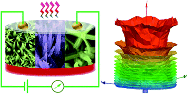
Higher dimensional ZnO nanoforms offer unprecedented advantages over their low dimensional counterparts in emerging technologies. This motivated the researchers to design ZnO hierarchical architectures which are expected to offer performances improved to device benchmarks. Starting from 1D ZnO nanospike arrays, hierarchical cactus and tree-like ZnO arrays with increasing branching and complexities have been grown via a simple wet chemical approach in ambient conditions. The zero thermal budget, large area of fabrication and absence of any structure-directing agents are the novel highlights of the current synthesis protocol. Cathodoluminescence spectroscopic investigation reveals a gradual increment in defect constitution in these nanoforms with increasing structural complexity. The synthesized nanostructure arrays display promise in electron field emission owing to their structural uniqueness as indicated by field distribution calculations using ANSYS electromagnetic software. Furthermore, these higher order nanostructures are capable of detecting UV light with photocurrent gains as high as 2.21 × 10⁴.


Introduction

Geometrically intricate multiscale hierarchical configurations embrace one dimensional (1D) nanostructural building blocks by inheriting the intrinsic features of nanoscale singularities as well as exhibiting a highly activated surface area and the robust stability provided by two or higher level structures. They are of paramount significance to material chemists and technologists.1–3 Among these higher dimensional superstructures, dendritic and complex branched nano-architectures are of special significance owing to their large number of connection points which in turn offer resources for parallel associations and interconnection of functional components.4–6 Additionally, the high degree of complexity associated with these nanoforms provides broad applications in catalysis,7,8 photodetection,9 sensing,10 optoelectronics,11 field electron emission,12–15 photovoltaic devices16 etc. ZnO, with its vast morphological assortments, is possibly the most explored metal oxide in this respect, owing to its intriguing features like nontoxicity, biocompatibility, chemical and photochemical stability, electrochemical activities etc. Accordingly, these interesting ZnO hierarchies represent the main structural units used for the fabrication of several optoelectronic and electronic devices.17–23 Amalgamation of the nanoscale building blocks into these complicated complexes is generally attained via oriented aggregation, self-assembly, templating synthesis, sequential seeding and growth etc., where the adopted experimental pathways are hydrothermal, electro-deposition, physical vapor deposition, chemical vapor deposition (CVD), metalorganic CVD, wet chemical etc.24–32 Among these enlisted practices, the low temperature solution processed route is the most suitable for the creation of combinatorial architectures owing to several expedient features such as the nominal thermal budget, straightforward processing, easy fabrication etc. The other methods are not only expensive, but also require several stringent criteria and complex manipulations.7,33,34 Considering all the aforesaid factors, novel, effective and facile wet chemical routes for the fabrication of ZnO hierarchical nanostructures are highly desirable.

Going beyond the often used multistep seeding and growth protocols to achieve higher dimensional nanoforms,31,35 ZnO branch hierarchies have been realized in a facile manner where the nucleation for secondary evolution and subsequent growth has taken place in the same reaction. When unrestricted by any stringent criteria such as sequential seeding or the necessity for high temperature, this protocol can yield a large area of thin film in ambient conditions, thus highlighting its accessibility and simplicity over other reported methods. The compactness as well as the dimension of secondary branches in the nanostructures, a key parameter for their practical usage, can be tailored in a subtle fashion by manipulating only the zinc salt concentration. These morphology-tuned hierarchies have already been applied to the fabrication of field emitters and UV photodetectors and outperform the devices constructed with 1-D nanostructures, a de facto choice until now. In addition to the morphology, the intrinsic variation of the defect structures of these as synthesized nanoforms has been found to influence the field electron emission as well as the photoresponse characteristics. These ZnO hierarchical architectures with nano-branches and self-assembled junctions are not only applicable to electron emission or photodetection applications but are also appealing for other possible usages such as in sensors, solar cells, photocatalysts and so forth.

Experimental

Deposition of the nanospike and hierarchical nano-architectures was executed on both glass and ITO coated glass substrate. For the nanospike synthesis, two separately prepared 10 mL solutions of 2 M potassium hydroxide (KOH) and 0.25 M zinc nitrate hexahydrate (Zn(NO3)2·6H2O) were mixed together and transferred to a 30 mL borosilicate glass bottle. Thereafter, one analytical grade zinc foil (1 cm × 1 cm × 1 μm) rubbed with fine emery paper, along with a KMnO4 activated substrate (glass or ITO coated glass), were placed in the bottle and kept for 3 h in ambient conditions. Finally, the substrate was washed with an ample amount of D.I. water and dried at room temperature.

For realization of the nanospike based hierarchical architectures, the pre-synthesized nanospike coated samples were used as the substrate. The experimental conditions were similar to those described previously, except for the zinc salt and potassium hydroxide concentrations. Separate sets of experiments were performed by varying the amount of zinc salt while keeping the KOH concentration fixed. Subsequent treatment with 0.13 M zinc nitrate and 1 M KOH favored nominal geometrical complex structure formation over nanospikes, whereas reaction with 1 M KOH and a higher zinc salt concentration (0.18 M) resulted in more complex nanoforms.

Characterization

Please see the ESI.

Results & discussion

Morphological & structural analysis

Fig. 1a displays the low magnification FESEM image and wafer scale synthesis (inset of Fig. 1a) of the ZnO nanospikes. The high resolution image (Fig. 1b) reveals that each individual nanospike possesses a smooth side surface and hexagonal building blocks, having an average length ∼1 μm and diameter ∼100–200 nm from top to base. The modification of the nanospikes in ambient conditions via successive wet chemical techniques leads to morphological changes in the pristine nanospikes; the corresponding microscopic images are shown in Fig. 1c and d. In complete contrast to the original nanospikes, tiny spines grow sparsely in a radial direction over the nanospike backbone and form a “cactus” like morphology in the low zinc salt concentration-assisted modification reaction. These spines have average diameter ∼10–30 nm from tip to base, and lengths ranging from 40–60 nm display an epitaxial relationship with the parent nanospikes (Fig. 1c). Instead of short sprouted spines, the subsequent chemical treatment of the original nanospikes with the higher zinc salt concentration promotes the formation of a nanostructured “pine tree” like robust branched network (Fig. 1d). Similar to the cactus like hierarchy, here the secondary branches are also generated in a radial fashion over the hexagonal prismatic nanospike facets. However, converse to the cactus formed hierarchy, higher dimensional aspects of the branches are found in this case; the average length as well as the top-base diameters are increased to ∼350 nm and ∼25–75 nm respectively (Fig. 1d). Henceforth, we will denote the parent sample simply as the nanospike and the low and high zinc salt-assisted modified hierarchical samples as the nanocactus and nanotree respectively.
image file: c5ra12838b-f1.tif
Fig. 1 FESEM images of the synthesized ZnO (a and b) nanospike (low and high magnification) (c) nanocactus and (d) nanotree; the inset shows the wafer scale synthesis.

The TEM analysis of the samples reveals the detailed surface morphology and structural information for the as prepared ZnO nanostructures. The inset of Fig. 2a shows a TEM image of a single ZnO nanospike having an average length ∼500 nm with a lateral dimension of ∼10–70 nm from top to base. A precise observation depicts the smooth side surfaces of the nanospikes where traces of other secondary growth is completely absent. The high-resolution transmission electron microscopy (HRTEM) image of the nanospike (Fig. 2a) with its distinct parallel lattice fringes indicates good crystallinity, and the interplanar spacing of 0.26 nm agrees well with that of the (001) plane of hexagonal wurtzite ZnO.36 Further, the selected area diffraction (SAED) pattern comprising bright circular spots confirms the single crystalline nature of the nanospikes (Fig. 2d). Several secondary branches radiating outwards with different dimensions appear over the pristine nanospikes to form the nanocactus and nanotree morphologies which are evident from the insets of Fig. 2b and c. For the nanocactus, low dimensional blunt branch nanospikes over the primary nanospikes are evident from the TEM image (inset of Fig. 2b). Conversely for the nanotree, secondary outgrowths with higher dimensionality are apparent from the corresponding TEM image (inset of Fig. 2c). In spite of their discernible dimensional differences, both the secondary nanocactus and nanotree branches maintain high crystallinity and are formed from the same functional material (ZnO), as manifested by the corresponding HRTEM images and SAED patterns (Fig. 2e and f and their insets).


image file: c5ra12838b-f2.tif
Fig. 2 TEM and HRTEM images and corresponding SAED patterns of the synthesized samples.

X-ray diffraction (XRD) patterns of the as synthesized samples with their different geometrical complexities are presented in Fig. 3a. All peaks in the diffraction patterns can be indexed with the hexagonal wurtzite phase of ZnO (JCPDS card no. 36-1451) with lattice constants of a = 3.25 Å and c = 5.21 Å. The absence of any other diffraction peaks conclusively excludes the possibility of impurity phases and indicates the phase purity of the synthesized samples.


image file: c5ra12838b-f3.tif
Fig. 3 (a) XRD patterns of the synthesized products; XPS spectra of (b) O 1 s, (c) Zn 2p, and (d) survey for the nanotree sample.

Along with XRD analysis, an X-ray photoelectron spectroscopy (XPS) investigation of a reference sample (nanotree) was further executed to investigate the surface composition of the products. Referencing the C 1s spectra at 284.6 eV, all the binding energies were energy corrected. A typical asymmetric O 1s spectrum corresponding to the nanotree sample is shown in Fig. 3b which can be deconvoluted to three peaks. The first and the most intense peak at binding energy ∼529.7 eV is accredited to the normal wurtzite structure of zinc oxide37 whereas the second one peaking at ∼531.1 eV relates to the O2 ion in the oxygen deficient region.38 A further peak at higher binding energy ∼532.2 eV is associated with the O2 of OH or H2O species39 which is almost inevitable with a chemically processed ZnO nanostructure irrespective of its state i.e. powder or thin film form.40 Finally, the Zn 2p spectrum in Fig. 3c with two highly intense peaks at 1022.5 and 1045.5 confirms the doublet formation and presence of Zn2+ only in the sample.41 The presence of no other impurity related peaks in the survey spectrum in Fig. 3d corroborates the XRD results.

The surface area, a vital structural parameter of nanostructure, strongly depends on morphology. In our samples, the geometrical intricacy increases gradually so there should be an obvious variance in their surface area. Fig. 4a–c shows the nitrogen (N2) physical adsorption–desorption isotherms for the ZnO nanostructures. The Brunauer–Emmett–Teller (BET) surface area of the nanospike, nanocactus and nanotree are found to be 34.461, 49.856 and 68.576 m2 g−1 respectively. Such results indicate enhanced N2 adsorption by the hierarchical nanostructures and a maximum surface area for the nanotree sample.


image file: c5ra12838b-f4.tif
Fig. 4 N2 gas adsorption–desorption isotherms of ZnO (a) nanospike, (b) nanocactus and (c) nanotree.

Cathodoluminescence study

Cathodoluminescence (CL) is an effective tool for probing the optical features of nanomaterials and reveals the spatial distribution as well as the interconnection between the sample morphology and the luminescence.42 Room temperature CL spectra of the synthesized ZnO nano-architectures recorded at an accelerating voltage of 1 kV are presented in Fig. 5a. CL spectra for nanospike, nanocactus and nanotree samples comprise two characteristic peaks, one narrow peak in the UV region around ∼382 nm and a broad emission band centered around ∼550 nm. The UV emission is accredited to a near band edge transition of wide band gap ZnO,43 while the visible emission is associated with different deep lying defects in ZnO, such as oxygen vacancies with different charge states, zinc vacancies and interstitial zinc etc. For ease of comparison of the defect related emission, all the UV peaks are normalized and presented in the same figure. It is also confirmed that the visible emission peak around ∼550 nm arises due to the presence of oxygen vacancies, and the intensity of the emission peak is associated with the vacancy concentration; the higher the vacancy concentration, the greater the intensity of peak.44 In the CL spectra, the intensity of the defect related emission peak is remarkably increased with the growth of higher degree secondary branches and such enhancement is related to the degree of oxygen vacancies. As oxygen vacancies mainly reside on the nanostructure surfaces, the higher surface area nanoforms should correspond to the presence of higher numbers of defects, and should exhibit an enhancement in visible emission. The hierarchical nanotree comprising dense and higher dimensional secondary branches possesses a high surface area compared to the nanocactus sample, as the latter consists of a sparse distribution of low dimensional secondary branches. On the other hand, the nanospike sample, devoid of any secondary branches, has a very low surface area compared to the previous two (as is clear from BET surface area values). In this aspect, the surface related defect concentration should follow the analogous order to the intensity variation of the visible emission related peaks.
image file: c5ra12838b-f5.tif
Fig. 5 (a) Room temperature CL spectra; (b) EDX spectra and atomic weight percentage; and (c) Raman spectra for the synthesized samples.

Furthermore, the intensity increment of the defect related emission peak with the increase of secondary branches in the hierarchical nanoforms is corroborated by their oxygen content ratio (determined from EDX measurement of samples) (Fig. 5b) and the corresponding elemental mapping (Fig. S1 in ESI). With the growth of secondary branches, the atomic percentage ratio of zinc to oxygen increases from 1.05 (nanospike) to 1.24 (nanotree) which indicates an oxygen deficiency in the hierarchical samples and thereby opens up the possibility of a higher number of defects.

The Raman spectra of the as grown ZnO nanostructures within the range from 90–600 cm−1 are shown in Fig. 5c. All the spectra are dominated by two sharp peaks, one at ∼98 cm−1 and the other at ∼437 cm−1. The former is designated as E2 (low) whereas the latter is labeled as E2 (high);43 these are also known as Raman active phonon modes which are the characteristic bands of hexagonal wurtzite phase ZnO. On the other hand, weaker peaks at ∼332 cm−1 and ∼389 cm−1 are related to E2H–E2L and A1(TO) modes respectively.45 Raman signals are very sensitive to the crystal quality as well as the defect structure of the nanostructure.46 Very close inspection of these spectra discloses that, with the increase of hierarchy in the nanoforms, the intensity of the Raman active mode at 437 cm−1 gradually decreases. Such a decrement in the intensity of Raman signal is connected with the presence of defects in the nanoforms. The increase in geometrical complexity and thereby the increase in the surface area of the nanoforms raises the defect constitutions (as is evident from the CL spectra). As a consequence of the enhanced defect constitution, the minimum intensity of the above mentioned Raman peak is observed in the nanotree sample and the maximum in the nanospike sample.46 Such results confirm that the changes in the defect constitution in the as prepared samples originate from structural modifications, and substantiate the CL results.

Plausible growth mechanism

The fabrication procedure for the nanostructured samples is schematically illustrated in Fig. 6. Based on the aforesaid structural evolution of the nanoforms, a plausible growth mechanism is proposed.
image file: c5ra12838b-f6.tif
Fig. 6 Schematic illustrating the synthesis procedure of ZnO nanospikes and hierarchy formation on glass/ITO coated glass substrates.

Zinc nitrate, on mixing with aqueous KOH solution, produces transparent zinc tetra hydroxide (zincket ions). Simultaneously, the zinc foil present in the same bottle, reacting with alkali, releases zinc ions in the same solution, as shown in the following reaction pathways:

Zn2+ + 4OH → Zn(OH)42−,

Zn + 2H2O + 2OH → Zn(OH)42− + H2

Continuous production of zincket ions in the solution via these pathways increases the super-saturation level; once the critical limit required to overcome the nucleation energy barrier is crossed, ZnO nuclei start to form homogeneously in solution as well as heterogeneously over the substrate. These mature to create the ZnO nanoform:

Zn(OH)42− → ZnO + H2O + 2OH

A wurtzite phase ZnO crystal is composed of stacked alternate polar planes of zinc (Zn2+) and oxygen (O2). This peculiar stacking leads to differences in the surface energies of crystal facets and results in the typical 1D growth of ZnO having the (002) plane at its top surface and non-polar planes at the side.

In additional to such preferential growth, the diffusion rate of freshly prepared zincket ions from the zinc foil plays a critical role in controlling the longitudinal diameter. A diffusion rate with a comparable or higher value than the growth rate results in a 1D nanostructure with uniform diameter due to a homogenous growth environment. On the other hand, the reverse circumstances create inhomogeneous growth surroundings for the 1D structure and result in a negative gradient of precursors from the base to the tip. Such diameter shrinkage along the length of the 1D structure consequently characterizes the nanospike morphology.

For secondary branch growth, nucleation of new crystal over the existing/pristine nanoform is indispensible and takes place spontaneously in the system in the absence of any additional seeding protocols. Once a nanospike coated substrate is introduced into a similar highly alkaline solution, it encounters a harsh environment which etches the side surface of the nanospike.47 As a consequence of such etching, the nanospike surfaces become rough and the possibility of defect incorporation in these nanoforms increases. It is experimentally confirmed that such defect centers serve as pin-points for nucleation.48 From these as formed nucleation sites, new secondary ZnO nanostructures start to grow after attaining the critical value, as discussed in the previous section. Small amounts of zinc precursor in the solution deter the growth of secondary branches to some extent and nanocactus morphology evolves. On the contrary, a higher zinc nitrate concentration results in higher dimensional nano-branches over pristine nanospikes.

Field emission

Based on the general perception that nanostructures which have a high aspect ratio and sharp edges are propitious for high field emission performance, we have investigated the field emission characteristics of the synthesized samples. In general, ZnO nanospikes bestow high emission currents as the emission performance benefits from their sharp tip geometry and aspect ratio.40 Therefore, geometrically modified nanospikes (i.e. nanospikes armed with multiple sharp protruding branches) are more likely to render a superior FE performance than the normal nanospikes. Field emission current density (J), plotted as a function of electric field strength (E), in Fig. 7a reveals a remarkably enhanced emission current for the hierarchies in comparison to the parent nanospike. ZnO nanospikes emit electrons with a characteristic turn on field (electric field required for extracting an emission current of 10 μA cm−2) of 3.01 V μm−1 which is downshifted to 2.03, and 1.44 V μm−1 for the nanotree and nanocactus samples, respectively. The threshold field values (electric fields required for extracting an emission current of 1 mA cm−2) for the nanotree and nanocactus samples are 5.09 and 4.10 V μm−1 respectively; however, the nanospike sample did not achieve the threshold value within the investigated electric field range. Such low field values for the nanocactus sample are comparable or superior to those of other inorganic semiconductors and thus signify its potential as an efficient cold cathode. Field emission, which is an electric field-assisted electron extraction phenomenon from cathode to anode through quantum mechanical tunneling, can be quantitatively explained by the Fowler–Nordheim (F–N) equation: J = (2E2/ϕ)exp(−3/2/βE). Here A and B are constants with values 1.56 × 10⁻¹⁰ (A V−2 eV) and 6.83 × 10³ (V eV−3/2 μm−1) respectively, and E = V/d (d is the anode-emitter distance). “β”, the geometrical field enhancement factor quantifying the electric field amplification ability of the emitter at the electron emitting site, can be estimated for the samples from the slopes of the linear ln(J/E2) vs. 1/E curves, known as the F–N plots (presented in Fig. 7b). The linear nature of the F–N plots in the high field region designates that the emission current originates from barrier tunneling of electrons. With the work function (‘ϕ’) taken to be 5.3 eV for ZnO, the estimated β values from the corresponding F–N plots were found to be 4473, 8771 and 14[thin space (1/6-em)]619 for the nanospike, nanotree and nanocactus samples respectively.49 Furthermore, we have investigated the electron emission behavior of the nanocactus at different electrode separations within the range of 120–180 μm with intervals of 30 μm. With increasing separation distances, the field values (both the turn on field and the threshold field) were downshifted very interestingly (Fig. 7c). For ease of comparison, we tabulated all the field values in Table 1. Furthermore, to check the merit of our samples, we have compared them with different sorts of field emitters and tabulated the data in Table S1 (ESI).
image file: c5ra12838b-f7.tif
Fig. 7 (a) JE plots and (b) corresponding F–N plots for the samples under investigation; (c) JE plots of the nanocactus sample with different vacuum gaps; (d) emission stability for all samples.
Table 1 FE parameters of the synthesized ZnO samples
FE parameters Nanospike Nanocactus Nanotree
Turn on field (V μm−1) 3.01 1.44 2.03
Threshold field (V μm−1) 4.10 5.09
β value 4473 14[thin space (1/6-em)]619 8771


Discernible differences in the field enhancement values among the synthesized products may result from several factors such as the emitter tip geometry, number of emission sites, neighbor emitter cross-talking (i.e. screening effect), crystallinity etc.40,50 An emission favorable geometry, i.e. a small radius of curvature for the tip, good vertical alignment and good crystallinity (as evident from the HRTEM and XRD images), ensures a moderate field emission performance from the nanospike. However in the nanospike, the maximum electron emission takes place from the tip as the smooth side surfaces lack adequate emission sites which in turn impede the emission performance. Now, as a consequence of the surface decoration with protruding secondary branches, nanospikes which have been transformed into nanocactus and nanotree shapes show a boosted overall emission performance. Such an increase can be explained with the help of two parameters, namely the number of emission sites and the geometrical arrangement. The appearance of numerous protruding branches with different degrees of vertical orientation on the smooth side surfaces of the nanospike results in large numbers of emission sites which impart an added advantage in electron emission.

Furthermore, this peculiar arrangement of branches over the nanospikes results in a two stage field enhancement. For branched geometry, the applied primary field is enhanced at the parent stems (ZnO nanospikes) which in succession acts as an effectively stronger applied bias at the base of branches and results in further enhancement.50 Based on this analogy, the nanotree sample, having larger numbers as well as higher aspect ratio emitters, should exhibit the highest field emission performance of the samples; however in practice, it produces a lower emission performance than the nanocactus. In nanotree sample, inter emitter closed proximity driven high field screening impede electron emission and produces a relatively low performance. The emission beneficial features in nanotree sample are overshadowed by the negative impact of the screening as the exponential dependence of screening over the emitter separation has much stronger influence on overall β value.51 Therefore, on the basis of screening alone, the emission current corresponding to the nanospikes should have been maximum; however, the registered converse behavior confirms the dominance of the adverse effect of low emission sites over screening. Thus, the nanocactus sample, which has optimal emitter density along with sizable inter-emitter separation, compensates for the detrimental influence of screening, and thereby offers the best performance. Furthermore, the oxygen vacancy concentration has a significant impact on electron emission as pointed out in our previous work.43 Surface defects, such as oxygen vacancies, acting as adsorption sites, create an additional surface potential barrier for the electrons and for greater numbers of vacancies, the potential barrier height becomes higher. Thus the nanotree sample with its higher oxygen vacancy concentration than the nanocactus (as is obvious from CL spectra) exhibits relatively lower characteristic field values than the latter. Finally, the anode-emitter separation-dependent field emission behavior as observed in our case is consistent with previous reports.12,52 With increased electrode distance, the effective emission area increases, and a greater number of electrons can reach the collector, which results in increased current density.53

Besides high emission current at lower electric fields, the temporal stability of emission currents over a long time is a decisive criterion of a practical electron emitter. To address this issue we have investigated the temporal variation of the field emission current with an initial emission current density of 1 mA cm−2 for all synthesized samples (Fig. 7d). The assessed fluctuations in the emission currents for the nanospike, nanocactus and nanotree samples are 12%, 9%, and 3% respectively. The nominal fluctuation as well as the absence of current degradation with time suggest that the nanotree sample has the highest electron emission stability. Such stability of the nanotree sample can be attributed to its high surface area, thereby its larger radiation area and lower resistance, which ease the heat dissipation procedure.54

Theoretical correlation

In order to verify our experimental field electron emission results, we have used a finite element method (ANSYS Maxwell simulation package) to investigate the local electric field distribution of the as synthesized samples. Initially, we designed 3D models of these nanostructures and chose the simulation keys in such a fashion that we could easily replicate the as synthesized morphology and make the simulation simple. Nevertheless, configurations of the models were based on the typical morphology and dimension of the three types of nanoforms in our experiments. For the nanospike sample, we considered a single nanospike with smooth side surfaces having length ∼250 nm and a diameter that changed from ∼50 nm to 10 nm from the base to the top, whereas for the nanocactus we decorated the parent nanospike surface with sparsely distributed low aspect ratio secondary branches having average length ∼50 nm and diameter ∼30–10 nm from base to top. Furthermore, for the nanotree sample, the number density of secondary branches as well as their dimension were increased. During all simulations, the inter-electrode separation (∼180 μm), dielectric constant (εZnO = 8.66),55 applied electric field (FM = 2.2 kV), type of collector etc. were maintained as the actual experimental parameters. A rainbow colored graphic in Fig. 8 represents the different electric field intensities, where the red and blue colors indicate the maximum and minimum field values respectively. The predominant confinement of the local electric field at the top of the nanospike and nanotree is obvious from the figure and will restrict their emission performances. On the contrary, the field emission distribution throughout the nanocactus surfaces will offer the highest electron emission for this sample and is prominent from the figure. Considering the presence of inter-emitter cross-talking, one can easily envisage inferior emission performance in the nanotree than the nanocactus sample and the analogous result is manifested by the simulation. Its performance was hampered to some extent by the screening of adjacent emitters, yet at the same time, the presence of a higher number of emitters was beneficial for the emission. Similar reasoning can explain the performance difference between the nanotree, with its higher number of emission sites, and the nanospike. Maximum field values from the model were found to be 1.96 × 10⁷ (F1), 5.10 × 10⁷ (F2) and 2.75 × 10⁷ (F3) for the nanospike, nanocactus and nanotree respectively. Field enhancement factors (β) for these samples can be calculated by taking the ratio of the maximum field values to the applied electric field i.e. (β = F1/FM). In all cases the applied electric field is the same, thus the ratio of β values is the same as the ratio of the maximum electric field values and is found to be 1[thin space (1/6-em)]:[thin space (1/6-em)]3.26[thin space (1/6-em)]:[thin space (1/6-em)]1.96 for nanospike[thin space (1/6-em)]:[thin space (1/6-em)]nanocactus[thin space (1/6-em)]:[thin space (1/6-em)]nanotree. Thus the simulated results predict the highest enhancement factor for the nanocactus and nominal values for the nanospike which is in good agreement with our experimental results.
image file: c5ra12838b-f8.tif
Fig. 8 Computed results overlaid with color mapping of the magnitude of the electric field distribution for (a) nanospike; (b) nanocactus; and (c) nanotree.

Fig. 9 illustrates the 3-dimensional simulated electric field distribution results based on the cactus model for different anode-emitter separations where d = 120, 150 and 180 μm. From the color plots, it is clear that the highest field emission current distribution is found for the largest vacuum gap which also upholds our experimental results.


image file: c5ra12838b-f9.tif
Fig. 9 Three dimensional perspectives of the ZnO nanocactus overlaid with computed electric field distributions at (a) 120, (b) 150 and (c) 180 μm anode-emitter separations.

UV response

Semiconductor nanostructures have already registered their supremacy as efficient UV detectors,56 as a consequence of their high specific surface area and uniquely designed surfaces which ensure an enhanced interaction probability of light-matter with the nanostructure surface.57,58 In this respect, the nanotree architecture has the potential to be a competent candidate for UV light detection as it possesses the highest surface area in comparison to the other synthesized nanoforms (see the BET results). The schematic of the photocurrent measurement configuration using two probe contacts (Fig. 10a) and linear current voltage (IV) characteristics of the nanospike sample measured in complete darkness (Fig. 10b) are shown. Such a linear IV dependence signifies the ohmic nature of the junction with deposited top gold electrodes. Prior to electrical measurement, all the samples were kept in complete darkness for a few hours to attain equilibrium. Photocurrent growth and decay of the fabricated detectors measured in ambient air at a fixed bias of 2 V in response to the switching on and off of UV light (350 nm) are presented in Fig. 10c. These transient response curves indicate the high UV sensitivity of the samples; before UV irradiation, the dark currents (Id) were 9.91 × 10⁻⁹, 4.57 × 10⁻⁹ and 1.63 × 10⁻¹⁰ A for the nanospike, nanocactus and nanotree samples respectively and on illumination, large changes in currents resulted, leading to elevated values of 3.26 × 10⁻⁷, 1.12 × 10⁻⁶ and 3.61 × 10⁻⁶ A for nanospike, nanocactus and nanotree respectively. The photocurrent gain (η) defined as the ratio of total photocurrent (Iph + Id) to dark current (Id) is only 3.38 × 101 for the nanospike while the same was enhanced by an order of magnitude to ∼2.46 × 10² for the nanocactus and further improved to 2.21 × 10⁴ for the nanotree sample. Additionally, the photocurrent growth and decay times (times taken for the increase of photocurrent by one order of magnitude after UV ON and decrease by one order after UV OFF) estimated from the curves confirm the fastest UV response for the nanospike and the slowest for the nanotree sample. Photocurrent switching behavior at the same bias voltage (2 V) was assessed as a function of time via periodic turning on and off of the UV source and is presented in Fig. 10d, which further signals the excellent reproducibility and stability of the devices. A very high decay time for the nanotree sample as compared to the others is obvious from the same figure. Even 10 min after the UV light is switched off, it has not returned to its initial dark value and so at the beginning of the next cycle there is some residual current i.e. the next cycle starts from a slightly high dark current value. The progressively increasing Id values in the consecutive cycles result in higher total photocurrent (Iph + Id) in any cycle compared to the previous one. Finally, for ease of comparison, all the UV parameters for the as synthesized samples are tabulated in Table 2 which indicates the response supremacy of the nanotree sample and the poorest response for the nanospike sample. Furthermore, a comparison is made in Table S2 (ESI) with respect to dark current, and photocurrent gain values of our sample with previously reported ones, to enlighten its importance in UV detection.
image file: c5ra12838b-f10.tif
Fig. 10 (a) Schematic of the photoconductivity measurement setup; (b) IV characteristics of the samples in the dark; (c) plot of the growth and decay of photocurrent measured with 350 nm UV excitation for all samples; (d) photoresponse cycles of all samples; (e) schematic of the UV detection mechanism of the ZnO nanostructure; and (f) band diagram for dark and illuminated conditions.
Table 2 BET surface area value and UV detector parameters of synthesized ZnO samples
Property Nanospike

image file: c5ra12838b-u1.tif

Nanocactus

image file: c5ra12838b-u2.tif

Nanotree

image file: c5ra12838b-u3.tif

BET surface area (m2 g−1) 34.461 49.856 68.576
Dark current (A) 9.91 × 10⁻⁹ 4.57 × 10⁻⁹ 1.63 × 10⁻¹⁰
Photocurrent (A) 3.26 × 10⁻⁷ 1.12 × 10⁻⁶ 3.61 × 10⁻⁶
Photocurrent gain (η) 3.38 × 101 2.46 × 10² 2.21 × 10⁴


Before reaching an understanding of the basis for the noticeable differences in photoconduction behavior of the synthesized samples, a detailed understanding of the photodetection mechanism in ZnO is essential.

In the dark, physisorbed and chemisorbed oxygen (O2) molecules on ZnO surfaces, through free electron capture in the conduction band, get ionized to O2 following the equation O2 + e = O2. Furthermore, simultaneous formation of a depletion layer by the upward band bending decreases the mobility of the rest of the carriers.56 The consequence of these two factors is the overall reduction in the dark conductivity of zinc oxide. Upon UV exposure (energy greater than or comparable with the band gap of ZnO), photoexcited electron–hole pairs are generated ( = e + h+). Following the as formed potential gradient, photoexcited holes transfer towards the nanostructure surface and are trapped by negatively charged oxygen ions through surface electron–hole recombination.56 On the other hand, photogenerated unpaired electrons with increased lifetime remain in the conduction band which in turn significantly increases the conductivity. Finally again in the OFF state, the O2 molecules re-adsorb on the nanostructure surface until the current is restored to the dark value.56

A schematic of the UV detection mechanism in the ZnO nanostructures in dark conditions and with UV illumination is presented in Fig. 10e. Furthermore, the schematic of the band diagrams in the dark and with UV illumination is displayed in Fig. 10f. As mentioned above, in the dark, the capturing of free electrons by the surface determines the current, thus nanostructures having the highest surface area should exhibit the lowest dark current due to the highest carrier annihilation. However, the high activity surface area of the nanostructures facilitates light matter interaction; thereby carrier generation is expected to be highest in these materials. From the BET results (Fig. 4), the maximum and minimum surface areas clearly correspond to the nanotree and parent nanospike respectively, i.e. the surface area of the nanostructures follows the order: nanospike < nanocactus < nanotree. Therefore the dark current and photocurrent gain should follow an analogous order, as both are mainly dependent on the variation in surface area. Additionally in ZnO, oxygen vacancies behave as donors, increasing the carrier concentration.56,59 Owing to the highest defect constitution (as shown by the CL spectra) the nanotree sample should exhibit the highest gain compared to the others. Such explanations for the variation of photocurrent gain and dark current, which consider structural parameters as well as intrinsic defects, are consistent with the observed results. Finally, the difference in transient response time can be accounted for by the variation in defects; generally the nanostructure with the greatest defect concentration should exhibit long growth and decay times, which is also consistent with the results observed.

Conclusion

In summary, a zero thermal budget, rationally developed eco-friendly approach is undertaken to generate zinc oxide hierarchical nanoform nanowires on a large scale. Starting with 1D nanospike arrays, higher dimensional nanoforms with different geometrical complexity are realized when the nucleation for secondary branch evolution and subsequent growth occur in the same reaction. The absence of post-growth high temperature modification steps as well as the large area fabrication capability are the hallmarks of this protocol. A comparative study reveals the highest field electron emission ability of the nanocactus sample and suggests that it is the most promising candidate among the samples for the design of cold cathode based devices. The nanotree sample emerged as the best photodetection candidate as a consequence of its morphological features as well as its enhanced number of defects. This work will open up new possibilities for applying a novel catalogue of hierarchical structures in a subtle manner and thereby will facilitate their usage in several types of nanoscale electronic and optoelectronic devices.

Acknowledgements

SP wishes to thank the Council of Scientific and Industrial Research (CSIR), the Government of India, for awarding her a Senior Research Fellowship (SRF) during the execution of the work. The authors also wish to thank the University Grants Commission (UGC) for financial support under the ‘University with Potential for Excellence (UPEII)’ scheme.

References

  1. H. Kim, S. Jeon, M. Lee, J. Lee and K. Yong, J. Mater. Chem., 2011, 21, 13458 RSC.
  2. H. Jung, S. H. Lee, J. Yang, M. Cho and Y. Lee, RSC Adv., 2014, 4, 7714 Search PubMed.
  3. U. K. Gautam, M. Imura, C. S. Rout, Y. Bando, X. Fang, B. Dierre, L. Sakharov, A. Govindaraj, T. Sekiguchi, D. Golberg and C. N. R. Rao, Proc. Natl. Acad. Sci. U. S. A., 2010, 107, 13588 Search PubMed.
  4. L. Xu, Q. Chen and D. Xu, J. Phys. Chem. C, 2007, 111, 11560 CAS.
  5. C. Gu, C. Cheng, H. Huang, T. Wong, N. Wang and T.-Y. Zhang, Cryst. Growth Des., 2009, 9, 3278 CAS.
  6. F. Zhao, J.-G. Zheng, X. Yang, X. Li, J. Wang, F. Zhao, K. S. Wong, C. Liang and M. Wu, Nanoscale, 2010, 2, 1674 RSC.
  7. H. Sun, Y. Yu, J. Luo, M. Ahmad and J. Zhu, CrystEngComm, 2012, 14, 8626 RSC.
  8. S. Pal, S. Maiti, U. N. Maiti and K. K. Chattopadhyay, CrystEngComm, 2015, 17, 1464 RSC.
  9. M. R. Alenezi, A. S. Alshammari, T. H. Alzanki, P. Jarowski, S. J. Henley and S. R. P. Silva, Langmuir, 2014, 30, 3913 CrossRef CAS PubMed.
  10. Y. Zhang, J. Xu, Q. Xiang, H. Li, Q. Pan and P. Xu, J. Phys. Chem. C, 2009, 113, 3430 CAS.
  11. C. Park, H.-M. So, H. J. Jeong, M. S. Jeong, E. Chang, W. S. Pippel and S.-M. Lee, ACS Appl. Mater. Interfaces, 2014, 6, 16243 CAS.
  12. S. Pal, S. Maiti, U. N. Maiti and K. K. Chattopadhyay, J. Mater. Chem. C, 2014, 2, 4005 RSC.
  13. S. S. Warule, N. S. Chaudhari, R. T. Khare, J. D. Ambekar, B. B. Kalea and M. A. More, CrystEngComm, 2013, 15, 7475 RSC.
  14. F. Xu, J. Chen, Y. Di, Y. Cui, J. Sun, L. Sun, W. Lei, C. Xu and W. Zhou, RSC Adv., 2012, 2, 11601 RSC.
  15. U. K. Gautam, L. S. Panchakarla, B. Dierre, X. Fang, Y. Bando, T. Sekiguchi, A. Govindaraj, D. Golberg and C. N. R. Rao, Adv. Funct. Mater., 2009, 19, 131 CrossRef CAS PubMed.
  16. M. Raja, N. Muthukumarasamy, D. Velauthapillai, R. Balasundaraprabhu, S. Agilan and T. S. Senthil, Sol. Energy, 2014, 106, 129 CrossRef CAS PubMed.
  17. D. Wu, Z. Gao, F. Xu, J. Chang, W. Tao, J. He, S. Gao and K. Jiang, CrystEngComm, 2013, 15, 1210 RSC.
  18. H. Kim and K. Yong, Phys. Chem. Chem. Phys., 2013, 15, 2109 RSC.
  19. S. Garry, É. McCarthy, J.-P. Mosnier and E. McGlynn, Nanotechnology, 2014, 25, 135604 CrossRef CAS PubMed.
  20. S. Singh, K. C. Barick and D. Bahadur, CrystEngComm, 2013, 15, 4631 RSC.
  21. P. Wang, X. Zhang, J. Wen, L. Wu, H. Gao, E. Zhang and G. Miao, J. Alloys Compd., 2012, 533, 88 CrossRef CAS PubMed.
  22. Z. Wang, J. Gong, Y. Su, Y. Jiang and S. Yang, Cryst. Growth Des., 2010, 10, 2455 CAS.
  23. C.-L. Hsu and S.-J. Chang, Small, 2014, 10, 4562 CrossRef CAS PubMed.
  24. M. Klaumünzer, M. Distaso, J. Hübner, M. Mačković, E. Spiecker, C. Kryschi and W. Peukert, CrystEngComm, 2014, 16, 1502 RSC.
  25. H. Zhang, R. Wu, Z. Chen, G. Liu, Z. Zhang and Z. Jiao, CrystEngComm, 2012, 14, 1775 RSC.
  26. L. Xu, Z. Li, Q. Cai, H. Wang, H. Gao, W. Lv and J. Liu, CrystEngComm, 2010, 12, 2166 RSC.
  27. Q.-P. Luo, B.-X. Lei, X.-Y. Yu, D.-B. Kuang and C.-Y. Su, J. Mater. Chem., 2011, 21, 8709 RSC.
  28. F. Xu, Y. Shen, L. Sun, H. Zeng and Y. Lu, Nanoscale, 2011, 3, 5020 RSC.
  29. Y. Chang, Y. Lu, M. Wang, Y. Long and R. Ye, Appl. Surf. Sci., 2013, 264, 687 CrossRef CAS PubMed.
  30. F. Xu, M. Dai, Y. Lu and L. Sun, J. Phys. Chem. C, 2010, 114, 2776 CAS.
  31. C.-T. Wu and J.-J. Wu, J. Mater. Chem., 2011, 21, 13605 RSC.
  32. R. F. Zhuo, H. T. Feng, J. T. Chen, D. Yan, J. J. Feng, H. J. Li, B. S. Geng, S. Cheng, X. Y. Xu and P. X. Yan, J. Phys. Chem. C, 2008, 112, 11767 CAS.
  33. K.-M. Kim, H.-R. Kim, K.-I. Choi, H.-J. Kim and J.-H. Lee, Sens. Actuators, B, 2011, 155, 745 CrossRef CAS PubMed.
  34. Z. Han, L. Liao, Y. Wu, H. Pan, S. Shen and J. Chen, J. Hazard. Mater., 2012, 217, 100 CrossRef PubMed.
  35. S. H. Ko, D. Lee, H. W. Kang, K. H. Nam, J. Y. Yeo, S. J. Hong, C. P. Grigoropoulos and H. J. Sung, Nano Lett., 2011, 11, 666 CrossRef CAS PubMed.
  36. U. N. Maiti, S. Maiti and K. K. Chattopadhyay, CrystEngComm, 2012, 14, 640 RSC.
  37. Z. Pan, P. Zhang, X. Tian, G. Cheng, Y. Xie, H. Zhang, X. Zeng, C. Xiao, G. Hu and Z. Wei, J. Alloys Compd., 2013, 576, 31 CrossRef CAS PubMed.
  38. R. Al-Gaashani, S. Radiman, A. R. Daud, N. Tabet and Y. Al-Douri, Ceram. Int., 2013, 39, 2283 CrossRef CAS PubMed.
  39. D. K. Kim and H. B. Kim, J. Alloys Compd., 2011, 509, 421 CrossRef CAS PubMed.
  40. U. N. Maiti, S. Maiti, S. Goswami, D. Sarkar and K. K. Chattopadhyay, CrystEngComm, 2011, 13, 1976 RSC.
  41. O. Lupan, L. Chow, G. Chai, B. Roldan, A. Naitabdi, A. Schulte and H. Heinrich, Mater. Sci. Eng., B, 2007, 145, 57 CrossRef CAS PubMed.
  42. H. Liu, L. Hu, K. Watanabe, X. Hu, B. Dierre, B. Kim, T. Sekiguchi and X. Fang, Adv. Funct. Mater., 2013, 23, 3701 CrossRef CAS PubMed.
  43. S. Maiti, U. N. Maiti, B. C. Behera, S. Pal and K. K. Chattopadhyay, J. Mater. Chem. C, 2013, 1, 4940 RSC.
  44. U. N. Maiti, S. Maiti, R. Thapa and K. K. Chattopadhyay, Nanotechnology, 2010, 21, 505701 CrossRef CAS PubMed.
  45. A. Umar, S. H. Kim, Y.-S. Lee, K. S. Nahm and Y. B. Hahn, Cryst. Growth Des., 2005, 282, 131 CAS.
  46. P. Ma, Y. Wu, Z. Fu and W. Wang, Adv. Powder Technol., 2012, 23, 170 CrossRef CAS PubMed.
  47. J. Wu and D. Xue, Mater. Res. Bull., 2010, 45, 295 CrossRef CAS PubMed.
  48. Y. Tong, Y. Liu, L. Dong, D. Zhao, J. Zhang, Y. Lu, D. Shen and X. Fan, J. Phys. Chem. B, 2006, 110, 20263 CrossRef CAS PubMed.
  49. U. N. Maiti, S. Maiti, T. P. Majumder and K. K. Chattopadhyay, Nanotechnology, 2011, 22, 505703 CrossRef PubMed.
  50. U. K. Gautam, X. Fang, Y. Bando, J. Zhan and D. Golberg, ACS Nano, 2008, 2, 1015 CrossRef CAS PubMed.
  51. S. Maiti, U. N. Maiti, S. Pal and K. K. Chattopadhyay, Nanotechnology, 2013, 24, 465601 CrossRef PubMed.
  52. A. Khademi, R. Azimirad, A. A. Zavarian and A. Z. Moshfegh, J. Phys. Chem. C, 2009, 113, 19298 CAS.
  53. A. N. Banerjee and S. W. Joo, Nanotechnology, 2011, 22, 365705 CrossRef PubMed.
  54. P. Feng, X. Q. Fu, S. Q. Li, Y. G. Wang and T. H. Wang, Nanotechnology, 2007, 18, 165704 CrossRef.
  55. Y. Yang, W. Guo, X. Wang, Z. Wang, J. Qi and Y. Zhang, Nano Lett., 2012, 12, 1919 CrossRef CAS PubMed.
  56. U. N. Maiti, K. K. Chattopadhyay, S. Karan and B. Mallik, Scr. Mater., 2010, 62, 305 CrossRef CAS PubMed.
  57. L. Peng, L. Hu and X. Fang, Adv. Mater., 2013, 25, 5321 CrossRef CAS PubMed.
  58. H. Liu, Z. Zhang, L. Hu, N. Gao, L. Sang, M. Liao, R. Ma, F. Xu and X. Fang, Adv. Opt. Mater., 2014, 2, 771 CrossRef CAS PubMed.
  59. M. Dutta, S. Mridha and D. Basak, Appl. Surf. Sci., 2008, 254, 2743 CrossRef CAS PubMed.

Footnote

Electronic supplementary information (ESI) available. See DOI: 10.1039/c5ra12838b

This journal is © The Royal Society of Chemistry 2015