
Fabrication and characterization of thin silicon solar cells produced by in-line spray coating
Efraín Ochoa-Martínez*a,
Cándido Vázquez†
b,
Daniel Solísa,
Itziar Hoces‡
c,
Iratxe Freirec,
Juan Carlos Jimenoc and
José Ramos-Barradoa
aUniversidad de Málaga, The Nanotech Unit, Depto. de Física Aplicada I, Spain. E-mail: e8am@uma.es
bIsofotón S.A, c/Severo Ochoa 50, PTA, 29590 Málaga, Spain
cInstituto de Tecnología Microelectrónica (TiM), UPV/EHU, Alda. Urquijo s/n, 48013 Bilbao, Spain
First published on 17th August 2015
Abstract
The present study addresses the metallization and characterization of thin (∼110 μm) crystalline silicon solar cells with a sprayed-on emitter prepared from orthophosphoric acid aqueous solutions and commercial spin-on dopants. The feasibility of such process especially for thin cells is analyzed, as well as the characteristics which derivate from the use of each precursor. The use of passivating and antireflective coatings on these devices has been essayed. The performance has been compared with that of cells prepared by an industrial process and featuring a traditional antireflective coating. Shunt resistance has been found to be the main limiting factor in order to increase cell efficiency, probably associated with microcracks due to the fragility of the cell. The characterization and the analytical model suggest that this method could produce cells exceeding 17% efficiency.
1. Introduction
The trend towards thinner substrates has always been a potential choice for the photovoltaic industry, and the fact that a decrease in wafer thickness would not harm cell efficiency1 but could even increase it2 has been known for a long time. Even though, it did not arose as a real option until the silicon shortage crisis around 2006, back in those years solar cells were still manufactured on 300 μm wafers, nowadays, the standard cell is around 180 μm and decreasing. The current industry roadmap signals 2025 as a tentative year when standard production should be fully established on 100 μm.3 However, the shift to thinner substrates has been mainly an issue of mechanical properties of the wafer and production yield, since it entails embracing innovative handling concepts, cell designs, interconnection and encapsulation solutions; the goal is a cost reduction by reduction of g/Wp of polysilicon, bibliography suggests that the trade-off between cell thickness and efficiency results in valuable cost reductions.4 Indeed according to the EPIA figures3 on silicon cost and the relative impact of the wafer on the final cell price, a decrease of 40% of the silicon material would imply a global reduction of approximately 8 billion US dollars in raw material costs.There have been thorough and fruitful efforts around thin crystalline cells, some of them have even been transferred to pilot lines,5 regarding the specific technology there are numerous approaches in literature for each process, first for producing thin wafers by stress-induced lift-off6 or diamond wire sawing,7 for handling and manipulation where the most suitable possibilities are the Bernoulli based handlers,5 and for the metallization with approaches which make use of standard screen printing for mono8 and bifacial thin cells;9 all these methods might be feasible at a laboratory scale for thin and even for ultra-thin solar cells;10–13 however, the right methods and technologies that will allow reaching thickness goals under a cost effective, high yield and high throughput process are still to be determined.
Other steps like the pn junction formation process have remained more or less unchanged during the last decades. The proposed method satisfies the current requirements of industry making use of a low cost, in-line and nearly contact-less process, and it could enhance production rate by avoiding the lost time for batch loading and unloading in the traditional POCl3 process. Noteworthy, spray-on technique is not new for thin film deposition on photovoltaic devices,14,15 there are even industrial prototypes,16 however, only few equipment manufacturers offer it, and even less producers have incorporated it in production lines. On the other hand, there have been successful results for H3PO4 based processes but on regular thickness cells,15 hence the novelty of this study for thin cells. This paper presents the results obtained from the application of a doping process previously optimized for the formation of phosphorus emitters,17 the same process with different liquid precursors has been used to produce boron emitters on n-type cells or back surface fields,18 however this work focuses on p-type cells. The goal is to identify the maximum potential of the different doping sources, allowing to compare commercial and self-made solutions on finished solar cells of around 110 μm.
2. Material and methods
2.1 Surface preparation and pn junction diffusion
The results presented in this paper cover the steps beginning from the phosphosilicate glass (PSG) removal until finishing and characterizing the device. The complete sequence from wafer to cell is shown on Fig. 1; however, the pn junction formation has been described in previous works.17 The cells feature a symmetric npn structure, obtained by spraying and drying on one side, and subsequently spraying and drying on the other, and have been produced from small size wafers cut from 156 × 156 mm2 wafers, obtaining samples of approximately 4 cm. After edge cut off the final size is of the cells is about 15 cm.2 There have been prepared 2 batches of samples: Batch 1 (B1) has been produced on 1–3 Ω cm, p-type cz-Si, with a thickness of 160 to 180 μm, thinned through an extended alkaline etching consisting on 10% NaOH at 90 °C, and a texturization step. The final thickness is in the range between 100 and 120 μm. Commercial doping source Phosphorofilm from Emulsitone and self-made Precursor C, a dilution of 4% (w/w) orthophosphoric acid with about 30% organic surfactants on deionized water,17 have been used as doping sources for this batch, the deposition of the doping source layer has been carried out in an in-line, self-made spray coating device. On the other hand, Batch 2 has been prepared as positive control on commercial textured substrates of ∼220 μm, whose pn junction has been produced by the POCl3 method resulting on 45 Ω □−1 emitters, these samples feature a SiNx anti-reflective coating (ARC). Given the characteristics of this reference batch, a good performance is expected, allowing the determination of the maximum potential of the metallization process under study.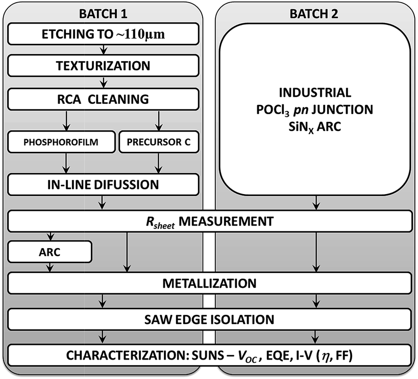 | ||
| Fig. 1 Crystalline silicon solar cell production process scheme. | ||
2.2 Metallization
The metallization and firing process has already been optimized, a brief description on the precise settings used in this work is shown below, further information can be found elsewhere.19,20 Prior metallization, samples were HF etched in order to remove the remaining PSG. Ferro 3347 silver paste has been used on the front face and 3398 aluminium paste on the rear face. The front grid design features 15 fingers with 2.5 mm of distance between fingers, and one 2 mm busbar in one side of the cell. The shaded area of the grid design is 15%, the back surface is metalized with a continuous layer.Paste drying and firing have been performed on a Despatch in-line infrared belt furnace. Several thermal profiles have been tried out in order to find the highest possible fill factor and efficiency. Finally, samples have been edge isolated with a diamond saw. An image of a finished cell can be seen in Fig. 2, where the front grid pattern is shown.
 | ||
| Fig. 2 Solar cells from Batch 1 (top left and bottom), and Batch 2 (top right). | ||
2.3 Anti-reflective coating deposition
There were several surface finishes essayed throughout the present work, from the bare as cut silicon, to a textured surface with or without ARC. The most basic approach consisted in thermal silicon oxide, for this purpose a thin thermal oxide has been formed at 800 °C in dry oxygen atmosphere during 30 minutes. A more advanced method implied the deposition of silicon dioxide by sputtering from a pure SiO2 target on an ATC Orion Magnetron Sputtering System from AJA International. The conditions used have been chosen in order to deposit a layer of approximately 110 nm. Finally, silicon nitride has been used in some cells. The layers have been deposited on an AK400 plasma enhanced chemical vapour deposition (PECVD) system from Roth & Rau.2.4 Device characterization
In order to classify and identify the properties of the best cells, the finished devices have been characterized according to their sheet resistance, I–V and suns–Voc response. Additionally, External Quantum Efficiency (EQE) and contact resistance (CORESCAN) analyses have been obtained for representative samples from each batch. The parameters obtained from the characterization have been used to produce a model of the cell with PC1D software,21 such model will allow to estimate the maximum potential of the cells once metallization and optical losses are overcome.3. Results and discussion
3.1 Batch 1 & Batch 2
The first batch of samples features a texturized surface aimed to decrease the optical losses. Thanks to texturization a reduction in reflectance of more than 20% has been achieved when compared with the as cut silicon, reaching reflectance below 10%. Furthermore, silicon oxide and silicon nitride have been tested as ARC. The ARC addition provides a significant enhancement mainly on the short wavelengths reaching reflectance values under 7%, similar to industrial results, while providing a passivating layer. These thin cells feature an average Rsheet of 38.2 and 30.1 Ω □−1 for the cells produced with Precursor C and Phosphorofilm respectively. It can be seen in Table 1, regarding the optimum firing settings, that most of the values of Voc lie in the range between 550 and 570 mV, with a substantial drop for the samples fired at 800 °C during 5 s, and 875 °C during 15 s, respectively the lowest and highest thermal budget profiles. Furthermore, shorter profiles are more appealing from an industrial approach, where any reduction in process time is welcomed.| Time (s) | Temperature (°C) | ||
|---|---|---|---|
| 800 | 850 | 875 | |
| 5 | 489.5 ± 26.8 | 551.8 ± 21.7 | 563.5 ± 20.5 |
| 10 | 561.0 ± 17.6 | 560.0 ± 18.4 | 564.0 ± 19.7 |
| 15 | 574.0 ± 14.5 | 564.7 ± 15.1 | 463.0 ± 27.3 |
The effect of firing conditions is shown on Fig. 3. It can be seen how above all the rest of processes, metallization is the single most important step in order to benefit from the full potential of a solar cell. Even when there are cells with high current density like B1-19 or B1-23, which are closer to 30 mA cm−2, they do not achieve higher efficiencies due to losses probably associated with a poor contact with the metallization grid, which results in a poor fill factor and, in the end, lower efficiency. In contrast, cells with lower current density result in higher efficiency, arguably because a better combination of emitter properties and metallization settings has been achieved.
 | ||
| Fig. 3 I–V curve of Batch 1 cells according to precursor and firing settings. | ||
Thin cells have been analysed before and after ARC deposition by suns–Voc technique, each control group consisted of at least 5 cells, the results are shown on Table 2. Dark and illuminated I–V curves have been fitted through MULTIV 2.3 software, allowing the determination of several relevant cell parameters. For the case of the samples shown in Fig. 3, the main difference can be found on the shunt resistance, samples B1-7 and B1-8 feature Rsh values of around 104 Ω cm−2 or even 105 Ω cm−2 for sample B1-19, while sample B1-23 barely reaches 103 Ω cm−2 denoting the presence of shunts on the cell and a higher leakage current. The rest of the cells have similar behaviours; the best cells feature shunt resistances between 104 and 105 Ω cm−2, while the worst cells are in the range of 102 to 103 Ω cm−2. Series resistance has been deducted as well from curve fitting; in this case the best cells are in the range of 0.25 to 1 Ω cm−2, while poor performing cells present Rs values between 1 and 10 Ω cm−2. An increase in the shunt resistance of almost 100% reaching values of up to 7.1 × 10³ for cells with SiO2 ARC is one of the most significant improvements, as shown in Table 2, confirming the shunts as one of the main reasons for the underperformance of the cells. Moreover, the significant decrease in the recombination velocity (S) and the increase on the effective lifetime (τ), reaching values of milliseconds denotes its passivating effect. Finally, the most relevant parameters of the cell, open circuit voltage, efficiency and fill factor are all increased. These results are in agreement with those obtained from industrial cells, where the addition of an ARC is known to boost efficiency around 0.2–0.5%abs. The residues of the emitter at the edge of the cells are among the most important process-induced shunts, they can be discarded due to the diamond saw isolation process used in this cells, however it is not possible to guarantee the absence of other sources of shunts like cracks, microcracks, scratches or Schottky-type shunts below grid lines due to the foreign species in the contact region.22
| Cell parameter | No ARC | With SiO2 ARC | With SiNx ARC |
|---|---|---|---|
| Rsh (Ω cm−2) | 3.6 × 10³ ± 9.36 × 101 | 7.1 × 10³ ± 1.28 × 10² | 6.0 × 10³ ± 1.02 × 10² |
| J01 (A cm−2) | 3.9 × 10⁻¹² ± 1.3 × 10⁻¹³ | 3.6 × 10⁻¹² ± 1.0 × 10⁻¹³ | 4.2 × 10⁻¹² ± 1.6 × 10⁻¹³ |
| J02 (A cm−2) | 1.4 × 10⁻⁸ ± 3.2 × 10⁻¹⁰ | 1.3 × 10⁻⁸ ± 4.9 × 10⁻¹⁰ | 2.6 × 10⁻⁹ ± 7.2 × 10⁻¹¹ |
| Seff (cm s−1) | 7.8 × 10² ± 3.9 × 101 | 1.4 × 10³ ± 7.4 × 101 | 1.2 × 10³ ± 5.4 × 101 |
| τeff (s) | 3.8 × 10⁻⁵ ± 1.5 × 10⁻⁶ | 1.0 × 10⁻³ ± 4.3 × 10⁻⁵ | 5.5 × 10⁻⁵ ± 3.1 × 10⁻⁶ |
| pVoc (mV) | 566 ± 28.3 | 574 ± 28.7 | 571 ± 19.6 |
| pEff (%) | 8.7 ± 0.3 | 9.6 ± 0.5 | 9.2 ± 0.3 |
| pFF (%) | 79.4 ± 2.4 | 81.8 ± 3.3 | 81.3 ± 2.8 |
On the other hand Batch 2, produced on industrial substrates featuring SiNx ARC provided by Isofotón and metalized with the same method as previous batches, has been analysed together with the rest of samples in order to give a clear idea of the weak points of the process and cell design. Table 3 shows the most relevant characteristics for the average and best cells, presented according to doping precursor. Neither the cell thickness nor the precursor, in the case of sprayed samples, has adversely affected the performance of the cells, on the contrary cells prepared with self-made precursors have performed as well as the cells from commercial doping sources and standard industrial POCl3 cells.
| Parameter (unit) | Batch 1 | Batch 2 | ||
|---|---|---|---|---|
| Phosphorofilm | Precursor C | POCl3 | ||
| Average | Voc (mV) | 562.3 ± 5.5 | 548.8 ± 36.0 | 528.1 ± 47.4 |
| Jsc (mA cm−2) | 20.6 ± 1.8 | 17.9 ± 1.2 | 22.8 ± 1.5 | |
| Eff (%) | 9.5 ± 1.5 | 7.5 ± 1.7 | 7.0 ± 1.6 | |
| FF | 80.8 ± 2.7 | 77.2 ± 2.9 | 70.1 ± 1.9 | |
| Best | Voc (mV) | 565.6 | 568.3 | 574.7 |
| Jsc (mA cm−2) | 25.7 | 24.1 | 23.8 | |
| Eff (%) | 12.2 | 11.4 | 10.7 | |
| FF | 82.1 | 81.4 | 74.1 | |
3.2 Comparison & discussion
Although the extraction of fundamental cell parameters through fitting the I–V curve can give information about the kind of fill factor problem, it is still impossible to relate it with a precise production process parameter. Furthermore, the fitting method is based on the assumption of a homogeneous emitter sheet and contact resistance. Reality is that contact resistance is a local property; other techniques like the transmission line method (TLM) can produce local contact resistance values at the expense of laborious sample preparation. On the contrary, through CORESCAN mappings23 several issues regarding the print quality and the sintering can be detected; for this technique, the cell is short circuited and current is generated by a light beam larger than the finger separation that is centred around the probe. The current has to be transported away from the point of generation, causing potential gradients over the surface of the solar cell. The specific contact resistance is proportional to the potential jump at the probe, in fact light intensity is chosen so that the registered potential value is equal to the contact resistance.Fig. 4 shows the contact resistance scanning (CORESCAN) of samples from an initial thick and untextured batch (B0), the thin textured batch (B1), and finally from the reference batch (B2). The mappings on the image show that cells from the first and second batch, B0 and B1, feature suitable contact resistance, which is quite interesting given the differences between the samples.
 | ||
| Fig. 4 Corescan of untextured thick cells (B0-14 and B0-68), textured thin cells (B1-7 and B1-8), and reference batch cells (B2-09 and B2-10). | ||
The thin cells from Batch 1, B1-07 and B1-08 share most of the characteristics, both have been prepared with Phosphorofilm and have an emitter of around 35 Ω □−1, they have been sequentially screen-printed, and fired at the same temperature, the only difference arises on the firing time, with 5 seconds for B1-07 and 10 seconds for B1-08. This kind of analysis is useful to detect issues on the screen printer, e.g., in both images the last finger is not conducting at all, probably due to an interruption in the connection to the busbar. Nevertheless, both samples feature a low enough contact resistance.
On the other hand, the two images from the reference batch B2 belong to samples which have an ARC already deposited before metallization, thus the firing settings used do not fit properly with the substrate characteristic, resulting in high contact resistance which might be the reason that despite having high Voc and Jsc the low fill factor of these cells, both below 50%, translates into an efficiency of around 10%, far below the potential of the substrate, which is used on standard industrial cells resulting in 17–18% efficiencies. These analyses show that the main constrain in order to have better efficiencies, is not linked necessarily to the emitter formation, given that even samples with a high quality emitter result in low efficiencies, evidencing the need to further optimize the metallization process. Nevertheless, the performance of cells prepared with self-made precursors under low-cost processes can compare with that of industrial process substrates.
The effect of the deposition of passivating and ARC layers is better described by the I–V curves of Fig. 5 top; in both cases the reduction of Rsh due to edge isolation is clear, moreover it is possible to see how the ARC sets the final device efficiency with a slight improvement for textured cells. Alternatively, the external quantum efficiency (EQE) of representative cells from each group has been characterized; it represents the fraction of incident photons that are converted to electric current for each wavelength, it allows determining the performance of each region of the cell based on the wavelength dependence on penetration depth.
 | ||
| Fig. 5 I–V curves after firing, edge isolation and ARC deposition for a thin textured cell of Batch 1 (top), and external quantum efficiency for cells of both Batch 1 and Batch 2 (bottom). | ||
The results show a poor performance on short wavelengths for the thin cells, probably due to the high doping of the emitters and the presence of a larger than expected dead layer, which creates more recombination centres in the surface; alternatively, the samples of Batch 2 prepared from POCl3 source with a less doped emitter (75 Ω □−1) and including an ARC layer perform better on short wavelengths but fail on the rest of the spectrum, probably due to the poor contact already discussed.
This is further confirmed on Table 3, where the most relevant cell characteristics are presented according to doping precursor (average and best cell). It can be seen that even when the reference batch outstands on current density, the final efficiency is below sprayed samples, the maximum cell efficiency value achieved has been 12.2% for a cell prepared with Phosphorofilm. Additionally, the results obtained from the reference batch indicate how the following work should be focused on the production of less doped emitters, which would enhance the performance by reducing the dead layer, reducing recombination rate and increasing lifetime. Nevertheless, metallization should be optimized as well in order to reduce the shading factor and improve contact.
Optical and SEM images have been acquired for the cells, Fig. 6 show the main characteristics of the metallization. On the top images it is possible to see the fingers of approximately 400 μm wide, which exceeds the usual industry values of 100 to 150 μm, increasing the shadowing factor and reducing active area; a closer view on the finger is available on the cross section of the middle image. The 15 μm thick finger, results in an aspect ratio below 0.04, again far below acceptable values of 0.3 to 0.4.
 | ||
| Fig. 6 Optical and electronic microscopy images of the screen printing metallization showing fingers on the different batches (top), a cross section of the finger (middle), and a cross section of rear contact (bottom). | ||
The thick rear layer, in many cases of more than 20 μm, covers the back surface of the cell, it is responsible for the positive electrical contact and is as well responsible for the bending of the cell due to the different thermal properties of the metallic compounds and the silicon, resulting in microcracks, cracks and cell breakage, especially on thin cells. The microcracks increase shunts, thus reducing cell efficiency; the cell breakage reduces process yield. The substitution of these thick layer metallization techniques is in the core of most of the current research on crystalline solar cells. Several options have been proposed for the rear contact, one of them is the substitution of the aluminium thick layer for an increase in boron doping concentration or local contacts.
3.3 PC1D simulation
The data gathered from the I–V curves and suns–Voc curves allows modelling the cell response. The simulations have been run on PC1D software, after fitting the results obtained with the current design, the individual effect of critical parameters is analysed, and following there will be presented two improved cell models which can show the full potential of the technology. There have been fixed parameters like cell texturing (front and rear), which was set on three microns with standard pyramid angle, additionally the characteristics regarding the front and back n-type diffused region are fixed.The measured and modelled data have been combined in three cases, the parameters are shown on Table 4 and the corresponding I–V curves on Fig. 7d. The first case is called present and represents the fitting of measured data to current results, the efficiency of 9.8% as well as most of the parameters are in agreement with the average values observed in the cells produced. The second case is called optimized and represents the cell behaviour after feasible improvements like the increase in Rsh and lifetime, which would lead to an efficiency of 14.2%, not far from the 12.2% obtained for the best cells. Finally, ideal case represents the theoretical maximum efficiency with the available technology; it assumes a significant decrease in Rs, the use of an optimized passivating/ARC layer and a less doped base, leading to an efficiency of up to 17.3%, matching the performance obtained with the same substrates through traditional production methods.
| Device | Current design | Optimized | Ideal |
|---|---|---|---|
| Front reflectance (%) | 10 | 10 | 5 |
| Series resistance (ohm) | 1 | 1 | 0.4 |
| Shunt resistance (ohm) | 1 × 10² | 1 × 10³ | 1 × 10⁴ |
| Thickness (μm) | 110 | 110 | 107 |
| p-type base doping (cm−3) | 1.0 × 10¹⁶ | 1.0 × 10¹⁶ | 3.0 × 10¹⁵ |
| Front: n-type (cm−3 peak) | 2.0 × 10²⁰ | 2.0 × 10²⁰ | 2.0 × 10²⁰ |
| Rear: p-type (cm−3 peak) | 1.5 × 10²⁰ | 1.5 × 10²⁰ | 1.5 × 10²⁰ |
| Effective lifetime (μs) | 10 | 100 | 1000 |
| Recombination velocity at F.S. (cm s−1) | 1 × 10⁶ | 1 × 10⁵ | 1 × 10⁴ |
| Results | Present | Optimized | Ideal |
|---|---|---|---|
| Jsc (mA cm−2) | 21.8 | 28.9 | 34.9 |
| Voc (mV) | 593 | 604 | 614 |
| Efficiency (%) | 9.8 | 14.2 | 17.3 |
 | ||
| Fig. 7 Effect of (a) thickness, (b) shunt resistance, and (c) recombination velocity on the main cell parameters, and (d) I–V curves for the existing, optimized and ideal cells, all obtained from the PC1D model. | ||
In first place the effect of cell thickness is shown on Fig. 7a, as already stated the effect of thickness is extremely dependent on the characteristics of the base material, therefore a highly doped and highly recombinant base results in significant efficiency losses with increasing thickness. An optimum point seems to be around 107 μm, in agreement with the value found in bibliography2,4 for the considered conditions. Other parameter that has been found to have a great influence on the results is the shunt resistance, the influence of Rsh variation is shown in Fig. 7b. It can be seen that an increase from the current 102 Ω (fitted value) to 104 Ω or 105 Ω could lead to an increase in efficiency of up to 2%abs, and although such values have been obtained for certain cells most of the results lied in the range between 102 and 103 Ω; as already discussed, there is not a direct source of shunt resistance, the microcracks due to cell bending, and shunting under the metallization are the most likely candidates.
Finally, given that the front surface passivation reduces recombination velocity and increases the efficiency, then through modelling on Sfront (see Fig. 7c) it has been found that, with the current cell characteristics, the deposition of a passivating layer which reduces the front surface recombination velocity from the current 106 cm s−1 to the range of 105 or 104 cm s−1 can lead to an increase of efficiency of another 2%abs. Furthermore, the antireflective effect provided for example by the passivating SiNx layer, has been found to have a lower impact on efficiency than the passivation. For the case of the cells presented in this paper, even though there were cells which featured a SiNx layer, it was not possible to realize the full passivating potential due to the lack of a posterior firing. Other parameters analysed which have shown a significant though smaller effect are the base doping and the carriers lifetime; either the reduction in base doping or the increase in carriers lifetime through passivation can lead to gains in efficiency of up to 1%abs.
4. Conclusions
There have been produced thin solar cells through a low cost process consisting on the deposition of doping sources by in-line spray-on. The best average efficiency was obtained for the cells produced from the spin-on dopant Phosphorofilm with 9.5%, followed by Precursor C cells with 7.5% efficiency. Moreover, the absolute maximum cells produced featured efficiencies of 12.2% for Phosphorofilm against 11.4% for Precursor C, denoting that self-made precursors can lead to cells with similar efficiencies than commercial solutions with lower cost and lower environmental impact once provided the right settings. The results indicate that the thickness reduction does not have any adverse effect on cell efficiency, given that thin cells have similar or larger efficiencies than standard thickness cells.External quantum efficiency measurements indicates poor performance on short wavelengths, for both textured and untextured cells, probably due to the high doping of the emitters. Current–voltage curve fitting has allowed identifying the main limitations on the current process. The low current density responds to the optical losses of such basic cells, for example the high shading factor of around 15% which reduces the cell active area.
Finally, even though the use of a traditional screen-printing metallization has allowed to test the potential of the sprayed emitters on thin cells, the thick rear layer of more than 20 μm covering the back surface of the cell is responsible for the bending and arguably microcracks, which increase shunts, thus reducing cell efficiency. The substitution of these thick layer metallization techniques is mandatory in order to achieve higher yield and efficiency. Optimization of the light trapping and passivation properties constitute the future steps which can contribute to enhance the efficiency of these cells. The analytical model suggests that the implementation of such improvements could lead to an absolute efficiency of about 17%.
Acknowledgements
This work has been supported by FEDER funds of the European Commission for scientific infrastructure, managed in collaboration with the Spanish Ministry of Science and Technology. The Spanish Ministry of Science with the research projects TEC2007-60996 and TEC2010-16700, Junta de Andalucía (Regional Andalucía Government) through the research group FQM-192 and ISOFOTÓN S. A. have also contributed. Technical support from S. C. A. I. of Universidad de Málaga is gratefully acknowledged.References
- P. Campbell and M. A. Green, J. Appl. Phys., 1987, 62, 243–249 CrossRef PubMed.
- S. W. Glunz, J. Benick, D. Biro, M. Bivour, M. Hermle, D. Pysch, M. Raüer, C. Reichel, A. Richter, M. Rüdiger, C. Schmiga, D. Suwito, A. Wolf and R. Preu, 35th IEEE Photovoltaic Specialists Conference PVSC 2010, Honolulu, United States, 2010 Search PubMed.
- SEMI-PVGroup, International Technology Roadmap for Photovoltaics (ITRPV) Results 2014, SEMI-PVGroup, 2015.
- K. Do, T.-h. Baek, M. Kang, S. Choi, G. Kang, G. Yu, J. Lee, J.-m. Myoung and H.-e. Song, Met. Mater. Int., 2014, 20, 545–550 CrossRef CAS.
- B. Terheiden, T. Ballmann, R. Horbelt, Y. Schiele, S. Seren, J. Ebser, G. Hahn, V. Mertens, M. B. Koentopp, M. Scherff, J. W. Müller, Z. C. Holman, A. Descoeudres, S. D. Wolf, S. M. de Nicolas, J. Geissbuehler, C. Ballif, B. Weber, P. Saint-Cast, M. Rauer, C. Schmiga, S. W. Glunz, D. J. Morrison, S. Devenport, D. Antonelli, C. Busto, F. Grasso, F. Ferrazza, E. Tonelli and W. Oswald, Phys. Status Solidi A, 2014, 212, 13–24 CrossRef PubMed.
- F. Dross, J. Robbelein, B. vandevelde, E. van Kerschaver, I. Gordon, G. Beaucarne and J. Poortmans, Appl. Phys. A, 2007, 89, 149–152 CrossRef CAS.
- X. Yu, P. Wang, X. Li and D. Yang, Sol. Energy Mater. Sol. Cells, 2012, 98, 337–342 CrossRef CAS PubMed.
- A. Upadhyaya, M. Sheoran, A. Ristow, A. Rohatgi, S. Narayanan and S. Roncin, IEEE 4th World Conference on Photovoltaic Energy Conversion, Hawaii, 2006 Search PubMed.
- J. C. Jimeno, J. Alonso, G. Bueno, R. Lago, I. Freire, L. Pérez, F. Recart, I. Hoces, N. Azkona and P. Sánchez-Friera, 22nd European photovoltaic solar energy conference, Milan, Italy, 2007 Search PubMed.
- S. Saha, M. M. Hilali, E. U. Onyegam, D. Sarkar, D. Jawarani, R. A. Rao, L. Mathew, R. S. Smith, D. Xu, U. K. Das, B. Sopori and S. K. Banerjee, Appl. Phys. Lett., 2013, 102 CAS.
- J. H. Petermann, D. Zielke, J. Schmidt, F. Haase, E. G. Rojas and R. Brendel, Prog. Photovoltaics, 2012, 20, 1–5 CAS.
- R. A. Rao, L. Mathew, S. Saha, S. Smith, D. Sarkar, R. Garcia, R. Stout, A. Gurmu, E. Onyegam, D. Ahn, D. Xu, D. Jawarani, J. Fossum and S. Banerjee, Conference Record of the 37th IEEE Photovoltaic Specialists Conference, Seattle, 2011 Search PubMed.
- J. L. Cruz-Campa, M. Okandan, P. J. Resnick, P. Clews, T. Pluym, R. K. Grubbs, V. P. Gupta, D. Zubia and G. N. Nielson, Sol. Energy Mater. Sol. Cells, 2011, 95, 551–558 CrossRef CAS PubMed.
- S. Barth, O. Doll, I. Koehler, K. Neckermann, M. Blech, A. Lawerenz, A. Edler, R. Kopecek and J. J. Schneider, Energy Procedia, 2013, 38, 410–415 CrossRef CAS PubMed.
- P. Kanti Basu, Z. Hameiri, D. Sarangi, J. Cunnusamy, E. Carmona and M. B. Boreland, Sol. Energy Mater. Sol. Cells, 2013, 117, 412–420 CrossRef CAS PubMed.
- Schmid-Group, Phosphor-Doper, http://www.schmid-group.com/en/photovoltaics/cell/phosphor-doper.html, accessed 04/08/2015, 2015.
- E. Ochoa-Martínez, C. Vázquez and J. Ramos-Barrado, Sol. Energy, 2014, 105, 139–146 CrossRef PubMed.
- E. N. Astorga, E. O. Martinez and J. R. R. Barrado, 9th Spanish Conference on Electron Devices (CDE), Valladolid, 2013 Search PubMed.
- I. Freire, PhD thesis, Instituto de Tecnología Microelectrónica (TiM), University of the Basque Country, 2010.
- R. Lago, L. Pérez, H. Kerp, I. Freire, I. Hoces, N. Azkona, F. Recart and J. C. Jimeno, Prog. Photovoltaics, 2010, 18, 20–27 CAS.
- D. A. Clugston and P. A. Basore, Conference Record of the 26th IEEE Photovoltaic Specialists Conference, Anaheim, United States, 1997 Search PubMed.
- O. Breitenstein, J. P. Rakotoniaina, A. S. H. van der Heide and J. Carstensen, Prog. Photovoltaics, 2005, 13, 645–660 Search PubMed.
- A. S. H. van der Heide, A. Schönecker, G. P. Wyers and W. C. Sinke, 16th European Photovoltaic Solar Energy Conference, Glasgow, United Kingdom, 2000 Search PubMed.
Footnotes |
| † Now at Monocrystal, 4/1 Kulakov pr. 355035, Stavropol, Russia. |
| ‡ Now at European Thermodynamics Ltd Debdale Wharf, Debadale Lane, Kibworth, Leicestershire, LE8 0XA UK. |
| This journal is © The Royal Society of Chemistry 2015 |