V. V. Shunaev,
G. V. Savostyanov,
M. M. Slepchenkov and
O. E. Glukhova*
Department of Physics, Saratov State University, Saratov, 410012, Russia. E-mail: glukhovaoe@info.sgu.ru
First published on 18th September 2015
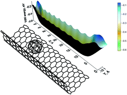
This paper studies the patterns of behavior of the fullerene C60 on graphene supported by an SiO2 substrate, taking into account the substrate topology and features of the electronic interaction between graphene and fullerene. It is found that the motion of the C60 molecule acquires a finite character when the substrate has a certain determined degree of curvature. We establish that such a character of motion occurs at a corrugation wavelength of 3.4 nm and wave-depth of 1.6 nm. The motion of the fullerene becomes more precise with deviations of tenths of an angstrom under an external electric field, which allows the motion of the fullerene to be manipulated along the trough. During the investigation of the electronic interaction between graphene and the C60 molecule it was found for the first time that the motion of the fullerene on graphene creates a small current that constantly changes due to the changing distance between the two objects. This physical phenomenon can be used as a physical principle for designing nanodevices.
There have been several earlier attempts to solve this problem. The influence of temperature on the character of C60 behavior on graphene has been considered in an array of works.4,5 It is well-known that a fullerene can be rather mobile either in a carbon nanotube or on graphene, freely moving even at low temperatures of several Kelvin.6,7 But this motion is unpredictable and uncontrollable due to temperature, all that is known is that with increasing temperature the motion velocity increases, which is evident. The fullerene’s ability to move freely suggests a method to manipulate its motion. The simplest method to manipulate fullerene motion is to apply an external electric field under the condition of fullerene charging, for example by encapsulating an alkali metal ion into a fullerene.8 In particular, in ref. 9 the authors made a numerical model of a C60 molecule with an encapsulated Fe− ion causing motion along a graphene nanoribbon in a zigzag of 157 × 2 nm2 along the X-axis to which an external electric field of 107 V m−1 was applied. It was found in the research process that under a constant field a fullerene would slide to the right edge of a graphene layer but would then drop off the edge of the layer because of insufficient velocity. Increasing the field strength to 2 × 10⁷ V m−1 allowed the fullerene to achieve the velocity required for overcoming the potential barrier of the nanoribbon edge. Taking into consideration the unidirectional character of a C60 molecule’s motion trajectory, as well as a field strength that cannot be realized in practice, it can be concluded that the problem of C60 motion trajectory manipulation by an external electric field is not solved.
Another proposed way of manipulating the fullerene’s behavior is the modification of the graphene atomic carcass, namely corrugation by displacement of graphene on a substrate of a predetermined form. On the one hand, the substrate has its own topology which influences the morphology of graphene; on the other hand, it also affects the properties of the graphene, for example its conductivity. It is shown in ref. 10 by means of atomic force microscopy that both single- and bilayer graphene almost exactly replicate the shape of a substrate with micron corrugation (groove width 1–2 μm). The depth of the graphene sag differs from the groove depth by just 2–5%. Only when the number of layers is 13 or more does the graphene sag disappear almost completely. Herewith, the authors point out that the adhesion of the graphene is just 0.044 eV nm−2, referring to the analytical calculations presented in ref. 11. These show that at a distance of 1 nm from the silicon dioxide substrate graphene interacts with a polar dielectric with an energy of 0.04 eV nm−2. The calculation has a purely electrostatic character and does not take into account the van der Waals interaction. This approach is not physical. In ref. 12 it has been experimentally proved by means of atomic force microscopy that adhesion of monolayer graphene is equal to 2.8 ± 0.1 eV nm−2 and for 2–5-layer graphene is equal to 1.9 ± 0.2 eV nm−2.
When considering fullerene–graphene interaction authors often solve only the problem of C60 molecule self-assembly on graphene. Consequently, they do not take into account the electronic interaction of the considered objects, which may be very important for the application of the obtained results to modelling of nanoelectronic devices. Ref. 13 uses the Monte Carlo empirical method to show that a group of C60 fullerenes located on corrugated graphene slide from the top of the corrugation into the valley thus taking up the most energetically favourable location. The authors propose this effect as one way to achieve molecular object self-assembly on graphene. But the authors do not illustrate the prospects of the discovered effect in nanoelectronics.
An attempt to consider the electronic interaction between graphene and a fullerene was made in ref. 14 using the DFT method. It showed the essential influence of Coulomb forces on the character of the interaction. It is important to note that the authors took into account the influence of the substrate: for example, the charge redistribution between graphene and a Cu(111) substrate leads to electron or hole conductivity of graphene. The authors also noted that the energy gap of a fullerene on graphene is 3.4 eV and that this exceeds the similar value for a fullerene on a metallic substrate. These results confirm the significance of studying the graphene + fullerene complex’s electronic structure for designing nanodevices based on such a complex.
According to the above mentioned facts the goal of this work is an investigation of the behaviour patterns of a single fullerene on graphene, with regard to the substrate’s influence and the adhesion of graphene, as well as a study of the graphene + fullerene complex’s electronic structure.
The force acting on atom α is presented in the following formula:
![]() | (1) |
Here the unperturbed Hamiltonian is determined by the expression:
H0μτ = 〈φαμ| + (nα0 + nβ0)|φβτ〉, α ≠ β,
| (2) |
is the radius vector of the corresponding nucleus; φαμ is the atomic orbital with moment μ on atom α; φβτ is the atomic orbital with moment τ on atom β; and the operators
and
define the kinetic and potential energies. We have previously applied this approach to construct the unperturbed Hamiltonian.16,19 Due to this approximation the atomic terms are located on the main Hamiltonian diagonal, and the interatomic elements which characterize a chemical bond are determined by means of the scaling function:
![]() | (3) |
ext we introduce an additional term which defines the energy of the bond dipole in the field. The expression
determines the vector of the dipole moment of the chemical bond, which is calculated by means of a preliminary calculation of the charge distribution of the atomic orbitals for each quantum state of the system. The energy of the bond dipole in formula (2) is represented by the second term. It is equal to zero when the external field is absent. The parameters p1,2,3,4 are determined by the type of interacting atoms as shown in ref. 16 and 20. We also take into account the energy of overlapping electron clouds of chemically non-interacting atoms of the two different molecular-atomic objects in the expression of the Hamiltonian. This energy is small but it should be considered in some cases to indicate possible charge transfer from one object to another. For this purpose we use the well-known expression for overlap integrals:18
![]() | (4) |
The second order term, Hμτ1, demonstrates the fluctuation of the charges on the atoms in the tight binding scheme. This term is an additional term to the off-diagonal elements of the Hamiltonian which take into account the charge shifts of different atoms and electron orbitals. This perturbed part of the Hamiltonian is given by
![]() | (5) |
![]() | (6) |
![]() | (7) |
The coefficients cτi are the coefficients of proportionality for the atomic orbitals φτ in the linear combination of atomic orbitals constituting the electron wave function with energy εi at the point with the radius vector
:
![]() | (8) |
εi represents the single-electron occupied level i; and ni is the occupation number. Functions of type
are determined by the value in the description of the exchange–correlation potential EXC. Each of them is determined by the following formula:
![]() | (9) |
![]() | (10) |
The van der Waals interaction energy is calculated by means of the known Morse function.21 The force arising due to the van der Waals interaction is represented by the penultimate term in formula (1). The last term in formula (1) defines the radiation force that is expressed by the Lorentz formula, where ε0 is the vacuum permittivity and c is the velocity of light. The temperature regime was modeled by the Berendsen thermostat algorithm and a collision algorithm.22 Simulation of the atomic motion process was carried out with a step of 0.1 fs.
The C60 fullerene was located on the graphene + substrate complex and simulation of the fullerene behavior was carried out for 100 ps at ∼300 K. The fullerene moved chaotically rolling in random directions along the curved substrate-supported graphene. We determined that under these conditions the fullerene made a complete rotation within ∼14 ps of movement. A general view of the complex and a trajectory of the fullerene’s mass center are shown in Fig. 2a and b.
![]() | ||
| Fig. 2 The fullerene on substrate-supported graphene: (a) general view; (b) trajectory of the mass center at T = 300 K during 100 ps. | ||
It is seen that by reaching the edge the fullerene is moving along it but does not leave the graphene. This is caused by the increase of the repulsive barrier of the van der Waals interaction of the molecule with substrate-supported graphene. Diagrams of the calculated interaction energy and fullerene velocity are presented in Fig. 3a and b. The interaction energy is calculated as the sum of the van der Waals interaction energy and the energy of the electron cloud overlap energy for the fullerene and graphene. Energy fluctuations are observed around the value of −1.36 eV at the average fullerene–graphene distance of ∼0.29 nm. It should be noted that according to our calculations the average energy of the van der Waals interaction is equal to ∼−0.85 eV and the energy of the electron cloud overlap is equal to ∼−0.5 eV, which suggests that the effect of the substrate should not be neglected in the study of the motion laws of fullerene on graphene. The velocity varies in the range of 10–75 m s−1. Such leaps in the velocity can be explained by the topological features of the graphene. In other words, depending on which structural fragments of graphene the fullerene moves over, it either speeds up or slows down. In particular, the most dramatic decrease in the rate was observed during the ascent of the fullerene up the walls of a hollow, and increases in the speed corresponded to the fullerene rolling down to the bottom of a hollow. In our case the character of the fullerene’s velocity change corresponded to the patterns of a mathematical pendulum’s velocity change. Its velocity falls to zero at the point of highest potential energy and reaches a maximum at the point with zero potential energy. Indeed, in the case of overcoming a potential barrier the fullerene slows down and then speeds up again.
![]() | ||
| Fig. 3 The fullerene on substrate-supported graphene: (a) change in the energy of interaction of C60 with graphene during its free motion at T = 300 K; (b) the velocity of the fullerene C60. | ||
The average value of the speed for the total simulation taking into account the traversed distance is equal to 58 m s−1. One can say that the change in the velocity of the motion has a disordered character. The increase and decrease of the speed can be clearly seen. Based on the minima the period of the velocity oscillation is equal to ∼20 ps.
To show the influence of the fullerene C60 on the graphene electronic structure we calculated the DOS distribution of the graphene + fullerene complex and the DOS of the separate fullerene and graphene. Fragments of the obtained DOS distribution near the HOMO-level for all three cases are shown in Fig. 4a and b. The red line corresponds to graphene DOS, green to the fullerene DOS and blue to the graphene + fullerene complex DOS which takes into account additional overlapping of fullerene and graphene electron clouds. Fig. 4 shows that the electronic structure of the graphene + fullerene complex looks like the electronic structure of separate graphene. The represented DOS fragment is very important from the view of estimating the complex’s electronic properties. It shows that during complex formation changes in the electronic structure of graphene occur exactly near the Fermi level (0 eV). We see that the intensity of the DOS increases match the DOS peaks of the C60 molecule (the vertical lines show it clearly). So it can be concluded that changes in the complexed graphene’s electronic structure happen due to the fullerene’s influence.
This effect is small but it can play a significant role in designing electronic devices based on the graphene + fullerene complex. In such devices an important role is played by electronic transitions between levels. To answer the question of how we can explain such a change in the DOS from the physical point of view, we calculated the distribution of the electron charge density (according to Mulliken method) of the fullerene and graphene at each time point. It was found that during the motion of the fullerene the distance to the graphene changes within ± 0.02 nm (from 0.27 nm to 0.31 nm), and the distribution pattern of the electron charge density on the fullerene changes too. Fig. 5 shows a graph (blue curve) of the change in the charge flowing from graphene to the fullerene during a time period of 0.5 ps (the charge was fixed with the step of 5 fs). The charge flowing to the fullerene is in the range 0.024–0.029e. On average, the charge on the fullerene is always in excess and equals −0.026e. The accuracy of the Mulliken method is 0.001e and allows observation of changes in the electron charge density in the noted interval. Another important conclusion that follows from the diagram is that during the motion the current flows from graphene to the fullerene. The current flowing within 10–20 fs can reach 14–17 nA. This pattern was confirmed by the results of multiple repetitions of numerical experiments with the same initial conditions that showed that fluctuation of charge takes place in all considered cases. This suggests that the graphene + fullerene complex is a single whole where a constant exchange of the charge is observed and the current exists. This current can be called molecular. Since the current is disordered, it cannot be the basis for the creation of an electronic device. But if one learns how to control it then one can design nanoelectronic devices with the molecular current as the energy source. The cause of significant fluctuations of the flowing charge is the rough topology of graphene, such that the fullerene is forced to approach and to move away from it. In addition, an important role is played by the fullerene’s rolling.
The adhesion energy slightly increased in comparison to an ideal crystal surface and was equal to 2 eV nm−2. The increase of the adhesion for the corrugated surface of the substrate was expected and justified by physical reasons. Namely, an ideal surface of crystal silicon dioxide does not exist in practice. Graphene interacts with defects of the crystal surface and the interaction energy rises. As shown in the Introduction, the experimental values for the adhesion for the monolayer are bigger than our estimates and are equal to 2.8 eV nm−2. Our calculation of the adhesion for the corrugated surface of the substrate is also equal to 2 eV nm−2, that is, higher than in the case of an ideal surface and closer to actual conditions. The energy increase is explained by the effect of the additional overlapping of the pi-electron clouds of the substrate and corrugated graphene atoms. We have shown earlier an increase in the energy of the interaction between hydrogen atoms and graphene with increasing graphene curvature.27 To confirm our hypothesis we compared the electronic structure of graphene on the corrugated substrate with the case of the ideal substrate. For the case of graphene corrugation and reduplication of the substrate’s topology a slight rehybridization of the electron clouds was observed. Fig. 6 shows the calculated DOS of graphene for three cases: for flat graphene, for graphene on the ideal substrate and on the corrugated substrate.
![]() | ||
| Fig. 6 Graphene on a substrate: density of electronic states of graphene in ideal and corrugated substrates. | ||
Fig. 7 shows atomic structures of graphene fragments on ideal and corrugated substrates. It is clearly seen that the main effect is caused by the curvilinearity of the substrate while the degree of the corrugation does not play such a role. In Fig. 6, the blue and green curves are practically the same but they are completely different from the red curve which corresponds to ideally flat graphene. The coincidence of the blue and green curves might be explained by a slight change in the electronic structure of graphene. On the basis of the calculation of the pyramidalisation angle distribution it can be concluded that the rehybridization of the pi-electron clouds with the sigma-electron is equal to about 2.02. This means that some electrons (of the atoms highlighted in red in Fig. 7) will eventually be in the sp2.02 condition. There is a slightly less noticeable rehybridization of the electron clouds of the neighboring orange colored atoms, which are sp2.01. In comparison, the maximum hybridization for graphene on the non-corrugated graphene substrate will be sp2.001.
![]() | ||
| Fig. 7 Fields of the atomic grid with rehybridized electron clouds (the maximum degree of rehybridization belongs to the atoms marked with red dots). | ||
The fullerene’s position in the corrugated graphene varies significantly. It moves within the groove. Fig. 8 shows a fragment of the substrate with the graphene nanoribbon and the fullerene at 300 K, and a diagram of changes in the interaction energy of the fullerene with changes in the environment, the speed of the fullerene and the trajectory of its mass center. For the case of the nanoribbon the character of movement is oscillatory: the fullerene rolls along the bottom of the groove from one end of the nanoribbon to the other without going beyond its track (Fig. 8b).
![]() | ||
| Fig. 8 Fullerene on the corrugated substrate at T = 300 K: (a) general view, (b) the trajectory of the mass center, (c) velocity changes, and (d) oscillations of the interaction energy. | ||
The movement of the fullerene becomes finite with one degree of freedom (it moves to one side or the other). The deviation from a straight line is only 0.5 nm. The speed and the change of the interaction energy of the fullerene with graphene are shown in Fig. 8c and d. As a result of the movement along the bottom of the corrugation the velocity varies with a clear periodicity although the average value remains the same as the temperature continues to be equal to 300 K. The periodicity of the velocity change is expected since the fullerene makes finite oscillations and its trajectory has pronounced oscillations near the line along the bottom of the corrugation as shown in Fig. 8b. The velocity maxima correspond to passage along the bottom, the minima to slow-downs at the walls of the corrugation. The interaction energy also changes. Its value ranges from −1.65 to −1.2 eV. The increase of the absolute value is explained by the nature of the interaction of the fullerene with graphene. Due to the increase of its corrugation the interaction energy also increases.
More visible energy fluctuations affect the magnitude of the charge flowing from graphene to the fullerene. In Fig. 5 the green curve reflects the process of the charge change within 500 fs, namely in one of the fragments of the movement process. The distinct dip in the graph is observed when the charge increases to −0.03e, which indicates the fullerene’s approach to the graphene and additional overlapping of the pi-electron clouds. Thus the current in the molecular complex reaches 16 nA. Overall, the picture of the current flowing between the fullerene and graphene does not change because there are no additional external effects on the fullerene and graphene.
A constant uniform electric field was applied in the direction of a straight line that was defined by the bottom of a corrugation. The motion of the fullerene should be directed along this line. We considered various cases of the electric field values for the Li+@C60 complex. All calculations, as was shown in section 1, were carried out taking into account the influence of the external field on the energy of the molecular complex and graphene, the interaction energy of the fullerene and the graphene pi-electron system, the van der Waals interaction of graphene and the substrate, as well as losses due to the emission of electromagnetic fields by the rapidly moving Li+@C60 complex.
Within the limits of 90–100 V μm−1 (the field lines are oriented along the bottom of the hollow) the Li+@C60 complex moves under the influence of the field just on the bottom of the groove with minimal deviation. When the fullerene reaches the edge of the graphene it is reflected from the edge by the repulsion of the van der Waals interactions and sometimes moves backwards. In order to understand the reasons for the fullerene’s behavior on the graphene sheet of this topology, the energy profile of the objects’ van der Waals interaction in the framework of the Lennard-Jones potential was calculated.30 Fig. 9 shows a fragment of the energy profile corresponding to the movement of the fullerene in a graphene hollow near the edge of the sheet. It is clearly seen that the edges of the graphene hollow map the energy profile and meet the energy barrier with the height of ∼0.6 eV, which prevents release of the fullerene to the edge of the surface. We can assume that for overcoming this energy barrier a fullerene needs to be additionally energized by an external electric field of more tension, or to have a greater electric charge.
![]() | ||
| Fig. 9 Energy profile of the van der Waals interaction of a fullerene with a graphene sheet. Maximum energy values correspond to the blue color, minimum to the green. | ||
Then, forced by the electric field, it turns back and moves to the edge. This situation is shown in Fig. 10a where the field strength is equal to 20 V μm−1, and the temperature is still 300 K. The increase in the interaction energy of the fullerene with graphene at the time of the reflection from the edge of the graphene is clearly seen in the energy diagram. Another situation is observed when the field’s strength increases to the critical value of ∼200 V μm−1, (Fig. 10b): the fullerene leaves the substrate-supported graphene under the field. The energy increases gradually and stops changing when the fullerene moves freely outside the graphene. Here, unlike all the previous cases without a field, the flow of charge during the motion of the fullerene under the field is only 0.007–0.012e/C60. The reduction of the flowing charge is explained by the fact that the graphene’s electronic structure changes under the electric field. There is a redistribution of the electronic charge on the atoms with an increase of the charge density at the edges. Apparently, this is why the flow of the charge to the fullerene is less than that outside the field. This is why charge transfer can be neglected in an electric field without any consequences for the calculation of the trajectory of the motion and the energy of the Li+@C60 complex.
It is also found that during the motion of the fullerene a small current flows between the graphene sheet and the fullerene. It changes all the time while the distance between the fullerene and graphene changes. We suggest that such small currents can be considered as molecular currents inherent to new carbon nanostructured materials, e.g. the graphene + fullerene complex presented here, and cannot be considered as traditional electric currents in conductors. This physical phenomenon can be used as a new physical principle for designing nanodevices.
| This journal is © The Royal Society of Chemistry 2015 |