DOI:
10.1039/C5RA12192B
(Paper)
RSC Adv., 2015,
5, 70172-70177
Improving interfacial electron transfer and light harvesting in dye-sensitized solar cells by using Ag nanowire/TiO2 nanoparticle composite films†
Received
24th June 2015
, Accepted 10th August 2015
First published on 12th August 2015
Abstract
Metallic Ag nanowires coated with a TiO2 nanolayer (AgNWs@TiO2) were employed as electron conductors in the mesoporous photoanodes (developed by TiO2 nanoparticles, P25) of dye-sensitized solar cells (DSSCs). Our results demonstrate that the AgNWs@TiO2 (in an optimized content of 3 wt% in the photoanode) improved the energy conversion efficiency (η) of the DSSC from 4.68 to 5.31% compared to the DSSC without AgNWs@TiO2 (pure P25). Such an improvement could be mainly attributed to the reduced TiO2/dye/electrolyte interfacial charge transfer impedance. To our surprise, the surface plasmon resonance (SPR) and light scattering effects of the nanowires were found to substantially boost the incident photon-to-electron conversion efficiency (IPCE) of such DSSCs. Regardless of the assembly techniques, our results demonstrate the possibilities of developing the photoanode with reduced interfacial impedance and superior light harvesting capability compared to the existing photoanodes in similar configurations by appropriately adjusting the AgNWs@TiO2 content in the photoanode with P25 based composites.
Introduction
Dye-sensitized solar cells (DSSCs) are one of the promising alternatives to silicon based solar cells due to their distinctive features such as low cost and easy manufacture.1,2 In DSSCs, the micro-to-nano structures of mesoporous photoanode thin films are the dominating factors in the photovoltaic performance. Conventional strategies for enhancing the performance of this system include increasing the total surface area, optimizing the film thickness, varying the porosity of the film, as well as incorporating the metal oxide nanoparticles with various crystal phases and tunable dopants.2–4
The slow electron transport and the inefficient light harvesting are the two crucial factors hindering the development of high performance DSSCs. In conventional mesoporous photoanodes comprising only TiO2 nanoparticles, the boundaries of particles or crystallites trap the electrons intensively and thus hinder the electron percolation in wide distance.5 It substantially increases the charge recombination probability of the photogenerated electrons with oxidized species (i.e., dye molecules and ions in redox couples), eventually resulting in the low output current density.6 To improve the electron transport and reduce the interfacial electron transfer impedance in the photoanodes, methods for reinforcing the interparticle connection such as TiCl4 post treatment,7 heat treatment,8 sol–gel modification,9 and micro-nano composites10 were implemented. Among these approaches, the composites incorporating with one dimensional conducting materials present distinguishing features including the development of direct electrical pathways for rapid electron transport and the profound mesoporous architecture for light scattering which enable the development of high performance DSSCs. Functional materials such as nanowires,11 nanotubes,12 nanorods,13 and nanofibers14 were hybridized with nanoparticles to achieve fast electron transport and high surface area in the preparation of photoanodes. The inefficient light harvesting in long and short excitation wavelength regions hinders the quantum efficiency and thus results in a significant loss in photocurrent of conventional photoanodes.15 Such constrain can be released by adding light scattering particles and nanomaterials with surface plasmon resonance (SPR) effects. The light scattering particles increase the photon scattering pathways in the photoanodes against the solar spectrum in long wavelength region.16 The nanomaterials with SPR effects preserve the incident solar radiations in short wavelength region.17 Both the two pathways improve the photon-to-electron conversion probabilities and thus the energy conversion efficiency of the DSSCs.
In this study, we added the TiO2 coated Ag nanowires (AgNWs@TiO2) into the conventional P25 TiO2 photoanode to improve both the interfacial electron transfer and the light harvesting in DSSCs. In this anode, the photogenerated electrons in conduction band of semiconductor will preferentially transfer to the metal due to the presence of forward potential gradient (barrier height at oxide to metal heterojunction) from oxide to metal domain.18 Meanwhile, this barrier height can restrain the charge recombination with outer oxidized species.19 In this circumstance, the presented metal–oxide composite (AgNWs@TiO2 in P25 photonanode) improved the energy conversion efficiency of DSSC from 4.68% to 5.31% in an optima case (3 wt% AgNWs@TiO2 to P25) comparing to that of DSSC with pure P25 photoanode. Such improvement could be a combination factor including the reduced TiO2/dye/electrolyte interfacial charge transfer impedance, the enhanced SPR in high energy solar spectrum, and the presence of light scattering effects of the nanowires in the photoanode of DSSCs. To clarify these mechanisms, a series of composite photoanodes with different metal loadings were incorporated in the DSSC devices with systematic physical structure and electrochemical characterizations.
Experimental
Materials
Silver nitrate (AgNO3, 99.8%), chloroplatinic acid hexahydrate (H2PtCl6·6H2O, 98.5%), and ethylene glycol (EG, 99.0%) were purchased from Showa. Titanium(IV) n-butoxide (TTNB, 99.0%), acetylacetone (AcAc, 99.0%), triton X-100, lithium iodide (LiI, 99.0%), iodine (I2, 99.5%), 4-tert-butylpyridine (TBP, 96.0%), and 3-methoxypropionitrile (MPN, 98.0%) were purchased from Acros. Polyvinylpyrrolidone (PVP, Mw = 360![[thin space (1/6-em)]](https://www.rsc.org/images/entities/char_2009.gif) 000) and ethanol (99.8%) were purchased from Sigma-Aldrich. Acetone (99.5%) was purchased from Tedia. Diethanolamine (DEA, 98.0%) was purchased from Hayashi. Commercial TiO2 (P25) powder was provided by Degussa. Polyethylene glycol (PEG, Mw = 20000) was purchased from Alfa Aesar. cis-Diisothiocyanato-bis(2,2′-bipyridyl-4,4′-dicarboxylato)ruthenium(II)bis(tetrabutylammonium) (N719), fluorine doped tin oxide (FTO) glass (TCO22-7, 2.2 mm, 7 Ω sq−1), and Surlyn (Meltonix 1170–60, 60 μm) were provided by Solaronix.
000) and ethanol (99.8%) were purchased from Sigma-Aldrich. Acetone (99.5%) was purchased from Tedia. Diethanolamine (DEA, 98.0%) was purchased from Hayashi. Commercial TiO2 (P25) powder was provided by Degussa. Polyethylene glycol (PEG, Mw = 20000) was purchased from Alfa Aesar. cis-Diisothiocyanato-bis(2,2′-bipyridyl-4,4′-dicarboxylato)ruthenium(II)bis(tetrabutylammonium) (N719), fluorine doped tin oxide (FTO) glass (TCO22-7, 2.2 mm, 7 Ω sq−1), and Surlyn (Meltonix 1170–60, 60 μm) were provided by Solaronix.
Synthesis of TiO2 coated Ag nanowires
The AgNWs were synthesized by a seed-mediate polyol reduction process.20 First, 20 mL EG was preheated at 160 °C for 1 h under continuous stirring. 2 mL H2PtCl6·6H2O/EG solution (0.123 mM) was then added into the preheated EG. The reduced small Pt would serve as the seeds for the crystal growth of AgNWs. After 10 min, 12 mL AgNO3/EG solution (0.1 M) and 12 mL PVP/EG solution (0.092 mM) were added drop-wise into the previous solution simultaneously. Subsequently, the heating temperature was held at 160 °C for 1 h under continuous stirring for the reaction. The as-synthesized AgNWs were centrifuged by using acetone to remove excess reagents and finally re-dispersed in 2 mL ethanol. To coat the TiO2 protective layer on the nanowire surface, the AgNWs/ethanol solution was added into the TiO2 precursor solution containing 8.86 mL TTNB and 2.82 mL DEA. This TiO2 coating reaction was carried out at ambient temperature for 24 h under continuous stirring. The as-synthesized TiO2 coated AgNWs (AgNWs@TiO2) were centrifuged and finally re-dispersed in the deionized water for the preparation of photoanode thin films.
Fabrication of DSSCs
For preparing the mesoporous thin films for photoanodes, the slurry containing 2 g P25, 2 g PEG, 10 mL deionized water, 0.4 mL AcAc, and 0.2 mL X-100 was prepared first. Different amounts of AgNWs@TiO2 (1 wt%, 2 wt%, 3 wt%, and 4 wt% to P25) were added into the slurry separately. The 10 μm-thick mesoporous thin films were coated on FTO glasses by spin-coating these slurries, and the spin-coated films were finally calcined under 450 °C for 30 min. For comparison, a 10 μm-thick pure P25 film without adding AgNWs@TiO2 was prepared by using the same procedure. For preparing the photoanodes, the as-synthesized thin films were immersed in a N719 ethanolic solution (0.4 mM) at ambient temperature for 24 h. The Pt-coated FTO glasses were fabricated to be the counter electrodes. The detailed fabrication procedure of counter electrodes is described elsewhere.21 A mixture of LiI (0.5 M), I2 (0.05 M), and TBP (0.5 M) in MPN solvent was prepared for the redox electrolyte. Finally, the photoanode and counter electrode were assembled into a sandwich-type cell with Surlyn spacer, and the electrolyte was injected after the assemblage. The working area of dye-anchored TiO2 films was set to be 0.25 cm2 (5 mm × 5 mm). As a result, DSSCs equipped with five different photoanodes, the pure P25 photoanode (P25) and the photoanodes with different amounts of AgNWs@TiO2 addition (1 wt%, 2 wt%, 3 wt%, and 4 wt%), were fabricated.
Characterization
The crystal structure of the AgNWs was characterized by using X-ray diffraction (XRD) conducted at the beamline BL-01C2 of the National Synchrotron Radiation Research Center (NSRRC, Hsinchu, Taiwan) with the X-ray wavelength of 1.0 Å. The morphology of the AgNWs, the AgNWs@TiO2, and the photoanode thin films were characterized by JEOL JSM 6330F scanning electron microscope (SEM) under 15 kV operating voltage and JEOL JEM 1230 transmission electron microscope (TEM) under 100 kV operating voltage. The UV-visible (UV-vis) spectrum of AgNWs was acquired by using Ocean Optics USB4000 UV-visible spectrometer with the USB-DT deuterium tungsten light source. For photovoltaic characterization, the DSSCs were illuminated under AM 1.5 by using Newport Oriel Sol3A Class AAA solar simulator with the light output of 100 mW cm−2, and the data were recorded by Keithley 2400 source meter. The electrochemical impedance spectroscopy (EIS) measurement was conducted by using Metrohm Autolab PGSTAT30 potentiostat/galvanostat under AM 1.5 illumination. The incident photon-to-electron conversion efficiency (IPCE) of the DSSCs was measured by using PV Measurements QEX7 measurement system.
Results and discussion
Morphology and crystal structure of AgNWs
The AgNWs with diameters around 100–150 nm and lengths of several microns were obtained characterized by SEM (see Fig. S1a†). These characteristics were consistently elucidated by using UV-vis absorption spectroscopy by matching the surface plasmon resonance (SPR) features to that of the Ag nanomaterials.22 In the UV-vis absorption spectrum (see Fig. S1b†), the two characteristic peaks centered at ∼352 and ∼382 nm could be assigned to the transversal SPR modes of the AgNWs.22,23 The absence of longitudinal and spherical SPR modes for Ag particles clearly indicated the formation of AgNWs with high aspect ratio and high purity. To determine the crystal structure, the XRD analysis was employed and the corresponding diffraction spectrum is shown in Fig. S1c.† As indicated, the diffraction peaks of (111), (200), (220), and (311) facets suggest the formation of face-center-cubic (fcc) structure. It is worth to note that the as-synthesized AgNWs possessed higher diffraction intensity ratio of (111) over (200) facet as compared to the normal Ag crystal depicting the preferential growth of its (111) facet.22
Morphology of AgNWs@TiO2 and photoanode thin films
To prevent the structural changes of AgNWs in the preparation of photoanode thin films and the operation of DSSCs, the as-synthesized AgNWs were coated by TiO2 via sol–gel process on the surface to form the AgNWs@TiO2 structure. As shown in Fig. 1, the microscope images of the AgNWs@TiO2 suggest that the AgNWs were covered by a TiO2 nanolayer with a thickness around 20–50 nm. The inset in Fig. 1 demonstrates the AgNWs/TiO2 interface. As observed, the rough TiO2 shell entirely attached to the AgNWs which implies the formation of the metal/semiconductor heterogeneous junction. Such surface coated TiO2 was verified to stabilize the nanowire structure during the thermal treatment24 and restrain the erosion by electrolyte containing I−/I3− (see Fig. S2†). After the calcination of the thin films, the AgNWs@TiO2 without morphological changes was observed to be buried in the mesoporous P25 thin film (see Fig. S3†). This implied the successful incorporation of AgNWs@TiO2 into P25 matrix. However, with increasing the amount of AgNWs@TiO2 in the thin film, the degradation of the film quality is destined (see Fig. S4†). The defects in the photoanodes, including the pores and the cracks, suppress the electron collection and transport efficiencies and thus reducing the photovoltaic performance of the DSSCs (discussed below).
 |
| | Fig. 1 The microscope images of the AgNWs@TiO2. The inset is the image of the AgNWs/TiO2 interface. | |
Electrochemical and photovoltaic characterization of DSSCs
The EIS measurement was employed to clarify the impacts of AgNWs incorporation on the internal resistances (likely the kinetics of charge transfer or recombination) at interfaces in DSSCs. Fig. 2 compares the Nyquist plots of electrochemical impedance spectra of DSSCs equipped with the pure P25 photoanode and the photoanodes containing different amounts of AgNWs@TiO2. These spectra were fitted according to the model described in the literatures25,26 and the obtained results are summarized in Table 1. As indicated, the impedance of both the electron transfer at TiO2/dye/electrolyte interface (R2) and the ion diffusion in electrolyte (WS) gradually decreased with increasing AgNWs@TiO2 contents in the photoanode to the maximum extent of 3 wt% (25% for R2 and 21% for WS). The substantially decreased R2 could be attributed to the facilitated interfacial electron transfer at TiO2/dye/electrolyte interface by AgNWs@TiO2 in the photoanodes. In this case, the photogenerated electrons tend to inject from TiO2 to AgNWs due to the lower energy level of Ag compared to the TiO2. This phenomenon was consistently revealed in the literatures.19 It is important to note that the redox and the electron transfer kinetics of the integrated components are highly correlated with each other in an electrochemical system (in our case, DSSC). It means that, with the improved electron transfer at the AgNWs/TiO2/dye/electrolyte interface and the facilitated electron transport in the AgNWs, the ion diffusion in the electrolyte could be facilitated as well (decreased WS). However, with further increasing the AgNWs@TiO2 to 4 wt%, the R2 and WS increased. This might be attributed to the declined film quality due to the excess one dimensional framework of AgNWs@TiO2 embedding into the P25 thin film with insufficient building block matrix in the photoanode (as revealed by SEM in Fig. S4†). It resulted in high density of defects with sub-micrometer size which sufficiently reduce the percolation threshold of the photogenerated electrons in the photoanode.
 |
| | Fig. 2 The Nyquist plots of electrochemical impedance spectra of DSSCs equipped with different photoanodes. The equivalent circuit is inset. Note that RS is the series resistance, R1 is the electrochemical reaction impedance at counter electrode, R2 is the charge transfer impedance at TiO2/dye/electrolyte interface, WS is the ion diffusion impedance in electrolyte, and CPE1, CPE2, and CPE3 are the constant phase elements of the capacitance corresponding to R1, R2, and WS, respectively. | |
Table 1 The electrochemical properties of DSSCs equipped with different photoanodes
| Photoanode |
RS (Ω) |
R1 (Ω) |
R2 (Ω) |
WS (Ω) |
| P25 |
12 |
11 |
28 |
14 |
| 1 wt% |
12 |
11 |
24 |
14 |
| 2 wt% |
13 |
13 |
23 |
12 |
| 3 wt% |
12 |
13 |
21 |
11 |
| 4 wt% |
13 |
11 |
26 |
13 |
The IPCE (Fig. 3a and b) and the corresponding photovoltaic efficiency (Fig. 4) were measured for disclosing the origins and pathways of photogenerated electrons of DSSCs with different AgNWs@TiO2 content in the photoanodes. The IPCE curves in Fig. 3a demonstrate the intrinsic light conversion efficiency of the experimental DSSCs. To elucidate the enhancement more clearly, the IPCE curve of DSSC with pure P25 photoanode was served as baseline and was subtracted from that of DSSCs containing AgNWs@TiO2 (ΔIPCE = IPCE − IPCEP25) and the corresponding curves are present in Fig. 3b. At the wavelength region around 475–550 nm, the absorption of N719 dye, the IPCE variation with different AgNWs@TiO2 content can be rationalized by the EIS analysis. Due to the facilitated electron transfer from dye to TiO2, the corresponding photon-to-electron conversion by the dye could be improved as well. With adding AgNWs@TiO2 up to 4 wt%, this conversion decreased owing to the increased interfacial impedance. For the wavelength region around 375–475 nm, the apparent IPCE enhancement was observed in all the DSSCs containing AgNWs@TiO2. This could be ascribed to the transversal SPR of the AgNWs. For the wavelength region around 550–750 nm, the IPCE enhancement was only observed in the DSSCs with high AgNWs@TiO2 content. Such enhancement could be ascribed to the synergistic effect of the light scattering and the longitudinal SPR of the AgNWs. Therefore, the transversal and longitudinal SPR of the AgNWs could trap the incident light locally for improving the light harvesting in short and long wavelength regions, respectively.22 On the other hand, the relatively huge structure of the AgNWs could scatter the incident light for increasing the light pathway in the photoanodes. The light scattering effect was observed to contribute to the IPCE enhancement at long wavelength region.16 Though the TiO2/dye/electrolyte interfacial impedance increased in the DSSC containing 4 wt% AgNWs@TiO2, both the SPR and the light scattering effects resulted from the excess AgNWs@TiO2 could still contribute to the IPCE enhancement.
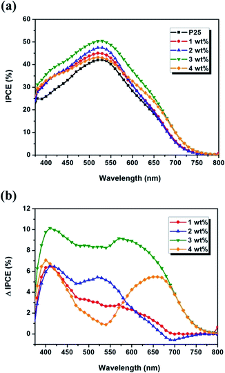 |
| | Fig. 3 (a) The IPCE and (b) the IPCE variation of DSSCs equipped with photoanodes containing different amounts of AgNWs@TiO2 as compared to the IPCE of the DSSC equipped with pure P25 photoanode (ΔIPCE = IPCE − IPCEP25). | |
 |
| | Fig. 4 The J–V curves of DSSCs equipped with different photoanodes. | |
Fig. 4 shows the photocurrent density–photovoltage (J–V) curves of the DSSCs with different AgNWs@TiO2 contents in the photoanodes and the obtained characteristics are summarized in Table 2. Accordingly, the DSSC containing 3 wt% AgNWs@TiO2 demonstrated the optimal energy conversion efficiency (η) of 5.31% among all samples. Compared to the DSSC equipped with the pure P25 photoanode (η = 4.68%) the photovoltaic efficiency was improved and could be accounted mainly from the increased photocurrent density (JSC) by ∼21.93% (from 9.85 to 12.01 mA cm−2). Such substantially improved JSC could be attributed to the reduced charge transfer impedance at metal to semiconductor (AgNWs and TiO2) interface and the improved light harvesting capability (including the light scattering effect and the SPR of Ag nanostructures) of our experimental nanocomposites comparing to the P25 photoanode. For the photoanode with 4 wt% AgNWs@TiO2, these two factors were severely diminished due to the overloading of one dimensional nanostructure in the P25 thin film with insufficient body to maintain the electron pathways. In this circumstance, the expanded pore structure degraded the film quality as elucidated by the gradually decreased fill factor (FF). The value of the FF reflects the extent of electrical and electrochemical losses occurring during the operation of the DSSCs. Since the measured series resistances (RS) of these DSSCs were nearly identical, the decreased FF was mainly attributed to the reduced shunt resistance (RSh) which is highly correlated to the manufacturing defects such as the photoanode thin film quality or the DSSC assembly techniques. The low RSh will result in the significant power loss of a photovoltaic system.
Table 2 The photovoltaic characteristics of DSSCs equipped with different photoanodesa
| Photoanode |
VOC (V) |
JSC (mA cm−2) |
FF |
η (%) |
| FF = PMax/(ISCVOC); η = VOCJSCFF/IIncident. Note that PMax is the maximum power, ISC is the short-circuit current, and IIncident is the intensity of the incident light. |
| P25 |
0.76 |
9.85 |
0.62 |
4.68 |
| 1 wt% |
0.78 |
9.51 |
0.62 |
4.60 |
| 2 wt% |
0.77 |
10.67 |
0.60 |
4.96 |
| 3 wt% |
0.75 |
12.01 |
0.59 |
5.31 |
| 4 wt% |
0.76 |
10.44 |
0.59 |
4.70 |
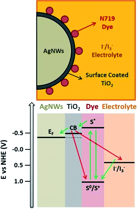
Taking all analytic results together, the schematic illustration of the AgNWs/TiO2/dye/electrolyte interface and the corresponding energy level diagram in the DSSC containing AgNWs/TiO2 are present in Scheme 1. Under illumination, the forward photochemical charge transfer processes, including the dye excitation, the electron injection from exited dye to TiO2, and the dye regeneration by I−/I3− redox couple, are triggered. Here, the Fermi level (EF) of the AgNWs/TiO2 heterogeneous junction should be equilibrated while metal is connected with semiconductor. Since the EF of metals such as Ag is more positive than the conduction band (CB) of TiO2, the photogenerated electrons injected from exited dye to TiO2 tend to further transfer to AgNWs rapidly.18 Moreover, as an effective charge separator, such metal/semiconductor heterogeneous junction could trap the electrons transporting in the AgNWs.19 Therefore, the backward electron transfer processes from TiO2, i.e., the charge recombination with oxidized dye molecules and I−/I3− redox couples, could be retarded effectively. The proposed thin film textures along with the probable electron transport pathways in the P25 photoanodes with and without AgNWs@TiO2 are illustrated in Scheme 2. As compared to the random diffusion pathways in the P25 photoanode, the electrons can transport directly via the AgNWs@TiO2 with the retrained charge recombination at the TiO2/dye/electrolyte interface in the photoanode containing AgNWs@TiO2. Also, both the SPR and the light scattering effects of AgNWs can contribute to the IPCE enhancement, so as to the improvement of the energy conversion efficiency.
 |
| | Scheme 1 The Schematic illustration of the AgNWs/TiO2/dye/electrolyte interface and the corresponding energy level diagram in the DSSC photoanode containing AgNWs@TiO2 under illumination. Note that the green arrows represent the forward photochemical charge transfer processes (i.e., the dye excitation, the electron injection from exited dye to TiO2, and the dye regeneration by I−/I3− redox couple), and the red arrows represent the backward electron transfer processes from TiO2 (i.e., the charge recombination with oxidized dye molecules and I−/I3− redox couples). | |
 |
| | Scheme 2 The Schematic illustration of the proposed thin film textures and the probable electron transport pathways in the P25 photoanode thin films with and without AgNWs@TiO2. | |
Conclusions
The photovoltaic performance of the DSSCs could be successfully improved by adding the AgNWs@TiO2 into the P25 photoanodes. Mainly resulted from the enhanced photocurrent density, the optimal energy conversion efficiency improvement was achieved by adding 3 wt% AgNWs@TiO2 to P25 (η = 5.31%) compared to the conventionally prepared DSSC using pure P25 photoanode (η = 4.68%). Characterized by EIS, the impedance of both the charge transfer at TiO2/dye/electrolyte interface and the ion diffusion in electrolyte in the DSSCs equipped with the photoanodes containing AgNWs@TiO2 was substantially reduced. This could be attributed to the facilitated electron transfer by adding AgNWs@TiO2. Also, observed in the IPCE characterization, the SPR and the light scattering effects of the nanowires were found to substantially boost the photon-to-electron conversion efficiency of such DSSCs in short and long excitation wavelength regions.
Acknowledgements
The authors would like to thank Professor Shih-Yuan Lu and his research group (Department of Chemical Engineering, National Tsing Hua University, Hsinchu, Taiwan) for the help in EIS measurement and analysis. In addition, the authors would like to thank the staffs of NSRRC for the help in synchrotron X-ray related measurements and analyses. The authors also acknowledge the financial supports from the National Science Council, project No. NSC 102-2113-M-007-013 (T.-L. Lin), the Ministry of Science and Technology, project No. MOST 103-2113-M-007-014-MY2 (T.-L. Lin) and MOST 103-2112-M-007-022-MY3 (T.-Y. Chen), and the Frontier Research Center on Fundamental and Applied Sciences of Matters of National Tsing Hua University (T.-L. Lin).
References
- B. O'Regan and M. Grätzel, Nature, 1991, 353, 737 CrossRef PubMed.
- A. Hagfeldt, G. Boschloo, L. Sun, L. Kloo and H. Pettersson, Chem. Rev., 2010, 110, 6595 CrossRef CAS PubMed.
- R. Jose, V. Thavasi and S. Ramakrishna, J. Am. Ceram. Soc., 2009, 92, 289 CrossRef CAS PubMed.
- C. J. Barbé, F. Arendse, P. Comte, M. Jirousek, F. Lenzmann, V. Shklover and M. Grätzel, J. Am. Ceram. Soc., 1997, 80, 3157 CrossRef PubMed.
- P. Docampo, S. Guldin, U. Steiner and H. J. Snaith, J. Phys. Chem. Lett., 2013, 4, 698 CrossRef CAS.
- K. Park, Q. Zhang, D. Myers and G. Cao, ACS Appl. Mater. Interfaces, 2013, 5, 1044 CAS.
- N. Fuke, R. Katoh, A. Islam, M. Kasuya, A. Furube, A. Fukui, Y. Chiba, R. Komiya, R. Yamanaka, L. Han and H. Harima, Energy Environ. Sci., 2009, 2, 1205 Search PubMed.
- S. Nakade, M. Matsuda, S. Kambe, Y. Saito, T. Kitamura, T. Sakata, Y. Wada, H. Mori and S. Yanagida, J. Phys. Chem. B, 2002, 106, 10004 CrossRef CAS.
- P.-C. Huang, T.-Y. Chen, Y.-L. Wang and T.-L. Lin, Thin Solid Films, 2014, 570, 268 CrossRef CAS PubMed.
- T. Y. Lee, P. S. Alegaonkar and J.-B. Yoo, Thin Solid Films, 2007, 515, 5131 CrossRef CAS PubMed.
- M. Law, L. E. Greene, J. C. Johnson, R. Saykally and P. Yang, Nat. Mater., 2005, 4, 455 CrossRef CAS PubMed.
- B. Tang and Y. Wu, J. Phys. Chem. B, 2006, 110, 15932–15938 CrossRef PubMed.
- B. H. Lee, M. Y. Song, S.-Y. Jang, S. M. Jo, S.-Y. Kwak and D. Y. Kim, J. Phys. Chem. C, 2009, 113, 21453 CAS.
- P. Joshi, L. Zhang, D. Davoux, Z. Zhu, D. Galipeau, H. Fong and Q. Qiao, Energy Environ. Sci., 2010, 3, 1507 CAS.
- T. G. Deepak, G. S. Anjusree, S. Thomas, T. A. Arun, S. V. Nair and A. S. Nair, RSC Adv., 2014, 4, 17615 RSC.
- S. Hore, C. Vetter, R. Kern, H. Smit and A. Hinsch, Sol. Energy Mater. Sol. Cells, 2006, 90, 1176 CrossRef CAS PubMed.
- J. Qi, X. Dang, P. T. Hammond and A. M. Belcher, ACS Nano, 2011, 5, 7108 CrossRef CAS PubMed.
- A. Takai and P. V. Kamat, ACS Nano, 2011, 5, 7369 CrossRef CAS PubMed.
- P. K. Sudeep, K. Takechi and P. V. Kamat, J. Phys. Chem. C, 2007, 111, 488 CAS.
- Y. Sun, Y. Yin, B. T. Mayers, T. Herricks and Y. Xia, Chem. Mater., 2002, 14, 4736 CrossRef CAS.
- C.-Y. Wu, Y.-T. Liu, P.-C. Huang, T.-J. M. Luo, C.-H. Lee, Y.-W. Yang, T.-C. Wen, T.-Y. Chen and T.-L. Lin, Nanoscale, 2013, 5, 9181 RSC.
- Y. Gao, P. Jiang, D. F. Liu, H. J. Yuan, X. Q. Yan, Z. P. Zhou, J. X. Wang, L. Song, L. F. Liu, W. Y. Zhou, G. Wang, C. Y. Wang, S. S. Xie, J. M. Zhang and D. Y. Shen, J. Phys. Chem. B, 2004, 108, 12877 CrossRef CAS.
- J. P. Kottmann, O. J. F. Martin, D. R. Smith and S. Schultz, Phys. Rev. B: Condens. Matter Mater. Phys., 2001, 64, 235402 CrossRef.
- P. Ramasamy, D.-M. Seo, S.-H. Kim and J. Kim, J. Mater. Chem., 2012, 22, 11651 RSC.
- C.-Y. Huang, Y.-C. Hsu, J.-G. Chen, V. Suryanarayanan, K.-M. Lee and K.-C. Ho, Sol. Energy Mater. Sol. Cells, 2006, 90, 2391 CrossRef CAS PubMed.
- W.-Y. Cheng, J. R. Deka, Y.-C. Chiang, A. Rogeau and S.-Y. Lu, Chem. Mater., 2012, 24, 3255 CrossRef CAS.
Footnote |
| † Electronic supplementary information (ESI) available: Characteristics of AgNWs, I−/I3− erosion test of AgNWs and AgNWs@TiO2, and photoanode thin film quality. See DOI: 10.1039/c5ra12192b |
|
| This journal is © The Royal Society of Chemistry 2015 |
Click here to see how this site uses Cookies. View our privacy policy here.