Temperature-induced work function changes in Mn1.56Co0.96Ni0.48O4 thin films

Chao Maab, Lei Wang*a, Wei Ren*a, Heyong Wangab, Jinbao Xua, Jianmin Luoabc, Liang Biana and Aimin Changa
aKey Laboratory of Functional Materials and Devices for Special Environments of CAS, Xinjiang Key Laboratory of Electronic Information Materials and Devices, Xinjiang Technical Institute of Physics & Chemistry, Chinese Academy of Sciences, Urumqi 830011, China. E-mail: wangl@ms.xjb.ac.cn; renw@ms.xjb.ac.cn
bUniversity of Chinese Academy of Sciences, Beijing 100049, China
cXinjiang Uygur Autonomous Region Academy of Instrument Analysis, Urumqi 830011, China

Received 17th June 2015 , Accepted 3rd August 2015

First published on 3rd August 2015


Abstract

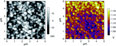
The variations of work functions in Mn1.56Co0.96Ni0.48O4 (MCN) thin films are investigated in the temperature range from 30 to 80 °C. The high resolution images of the contact potential difference (CPD) of MCN thin films were obtained through Kelvin probe force microscopy (KPFM) and the correlations between the work functions and temperatures were demonstrated through the imaginary part of the dielectric functions. The complex dielectric spectra are temperature dependent while their intensities have the inverse trend according to the work functions. The phenomenon can be interpreted by different chemical states that relate to the Mn3+ state.


Introduction

Transition metal oxides have attracted broad attention due to their rich physical phenomena such as metal–insulator transition, spin glass, high-temperature superconduction, and colossal magnetoresistance.1,2 These varied electrical and magnetic properties arise from the complex interactions between spin, charge, lattice, and orbit. Because of these unique properties, spinel oxides have found potential applications in electronic, optoelectronic, and spintronic devices. Manganese cobalt nickel oxide Mn–Co–Ni–O is one of typical spinel oxide materials with large negative temperature coefficient and widely utilized as temperature compensation devices, temperature sensor devices, surge protection devices, infrared detecting bolometer and so on.3,4 Mn1.56Co0.96Ni0.48O4 is the one with a specific composition, which has the minimum resistivity compared with the other Mn–Co–Ni–O oxides.5 It has been widely used in above mentioned applications since it responses different resistance in the varying temperatures. It is particularly suitable for the investigation of the correlation between its electrical properties and temperature.6 The work function of MCN film is an important property of the spinel oxides. However little is known about the effects of the ambient temperatures on the work functions of this material. Therefore, it is necessary to explore the effect of the ambient temperature on the work function of MCN film in order to design and control the electrical properties of MCN film for further applications.

Results and discussion

Fig. 1(a) shows the X-ray diffraction (XRD) pattern of MCN thin films deposited on Si substrates. There are six orientation peaks observed: (220), (311), (400), (422), (511) and (440). All of the diffraction peaks are identified as those from the spinel structure with the space group of Fd3m. The multi-orientation peaks indicate that the MCN spinel oxide films is poly-crystalline structured. Among these peaks, the (311) peak has the strongest intensity, indicating that the (311) orientation is preferred during the film growth. Fig. 1(b) illustrates the surface morphology of MCN thin films within an area of 5 × 5 μm2 at 30 °C by atomic force microscope (AFM) measurement. The film morphology is not smooth. The surface roughness of the sample is 7.8 nm. It is composed of numerous uniform-shaped particles with an averaged diameter of 200–300 nm, suggesting the island-growth mode during the film growth.
image file: c5ra11628g-f1.tif
Fig. 1 (a) XRD pattern and (b) AFM image of the MCN thin films.

The AFM techniques exploiting electrically conducting probes have been developed to measure electrostatic forces, charge distributions, voltage drops, capacitances, or resistances. The KPFM is based on the AFM and used to measure the CPD between the AFM conductive cantilever tip and the underlying sample.7,8 The CPD is equivalent to the surface potential voltage and can be described as the difference in the work functions between the probe tip (Φtip) and sample (Φsample), divided by the negative electron charge (−e). Knowing the tip work function, the sample work function can be determined correspondingly (according to the equation: eVCPD = ΦtipΦsample). In our KPFM measurement, an AC voltage is applied to the tip in order to generate oscillating electrical forces between the tip and the MCN film surface without grounding of the insulated Si substrate. Compensation of the electrostatic forces at this frequency is achieved by adjusting a DC bias to exactly match the CPD between tip and sample.9 The work function of the Pt tip compared to the standard sample is 5.5 eV. The images from the AFM in Fig. 2 thereafter show the effects of the temperature on the CPD values of the MCN thin films. The bright and dark areas identified in these images of the MCN islands correspond to a lower and higher work function respectively. The work function is obtained by averaging the work function values over a macroscopic area of the surface. The work function values obtained through above mentioned method in each temperature are presented in Fig. 3. It initially increases from 4.52 eV at 30 °C, and reaches a maximum value of 4.63 eV at 50 °C, and then decrease to a minimum value of 4.43 eV at 80 °C.


image file: c5ra11628g-f2.tif
Fig. 2 The CPD of MCN thin films in the temperature of (a) 30, (b) 40, (c) 50, (d) 60, (e) 70 and (f) 80 °C respectively.

image file: c5ra11628g-f3.tif
Fig. 3 The averaged work functions of MCN thin films as a function of temperature.

Work function (Φs) is regularly defined as the energy required for moving an electron from a material's Fermi level to the local vacuum level, i.e. Φs = E0EF. The first term corresponds to the energy of the electrons in vacuum, and the second term is the Fermi level.10 A material's work function may include two contributions: the electron chemical potential and surface dipole.11,12 The electron chemical potential represents the Fermi energy relative to the absolute vacuum level. The surface dipole represents an additional energetic barrier to removing an electron from the solid's surface.13

In order to explore the specific variations of electrons or cations, the imaginary part of the complex dielectric function of MCN thin films were measured by spectroscopic ellipsometry (SE) at different temperatures. Considering that the imaginary part of the dielectric function reflects the interaction of electrons with a peak of maximum absorption at resonant frequency in the visible range, the electronic transitions involving different cations or their concentration can be clearly demonstrated by the imaginary part of the dielectric functions.14 In our SE measurement, the Tauc–Lorentz (TL) oscillator dispersion formula was used to model a dielectric function to represent film properties. The four-phase model (air/surface roughness layer/MCN/Si) is built to characterize the dielectric function of the films.15 The TL dispersion function can be expressed as

 
image file: c5ra11628g-t1.tif(1)

Eqn (1) depends on four parameters: the transition matrix element A, the peak transition energy En, the broadening term C, and the band gap energy Eg. All these parameters are in units of energy.

Fig. 4 shows the imaginary part of the dielectric constants of MCN thin films under different temperatures. There found two broad absorption structures located at around 2.7 and 4.1 eV, respectively. The absorption structures could be related to the charge-transfer (CT) transitions involving 2p electrons of oxygen ions and 3d electrons of Mn ions, i.e. O2− (2p) → Mn3+ (3d4).16,17 The intensities of these absorption structures are related to the change of the electronic structures due to the concentration of Mn3+ ions.16,17 Surprisingly, we firstly found that the intensity variation trend of these SE absorption peaks with the temperature inversely matches the variation curve of the work function in Fig. 3. That is, the sample with the minimum absorption peak intensity (50 °C curve) has the maximum work function value and vice versa.


image file: c5ra11628g-f4.tif
Fig. 4 Imaginary part of dielectric functions of MCN thin films under different temperatures.

Although many factors may cause the variation of the work function, the concentration of Mn3+ on the topmost surface may play an important role in our experiment. A general correlation between the cation oxidation state and the oxide's work function has been noticed. Transition metal oxides in their less-oxidized forms tend to have lower work functions compared to their higher-oxidized analogue.13 And the trend is observed in our result that the increase of the low-electronegativity cations (Mn3+) might correspond to the decrease of the high-electronegativity cations (Mn4+), which leads to the decrease of a work function. Further evidence is that AFM detect the work function values within only several topmost layers of film surface, while SE is sensitive to the film thickness of sub-atomic layer. Both techniques reflect the parameter changes of the several top atomic layers, where the oxidation/de-oxidation of Mn3+ to Mn4+ might be possible within a temperature range of below 80 °C. However, further detailed exploration is still needed to explain the results.

Conclusions

The polycrystalline MCN thin film has been synthesized on the Si (100) substrate. The present results demonstrate the work functions and complex dielectric functions of MCN thin films are dependent on the temperature. The varying work functions with the different temperatures in MCN thin films could be ascribed to the changes of the chemical state due to the variation of Mn3+/Mn4+ content.

Experimental section

The MCN thin film was deposited on Si (100) substrates by traditional chemical solution deposition method. Mn(CH3COO)2·4H2O (AR, 99%), Co(CH3COO)2·4H2O (AR, 99%), and Ni(CH3COO)2·4H2O (AR, 99%) were selected as the raw materials with a mole ratio of Mn[thin space (1/6-em)]:[thin space (1/6-em)]Co[thin space (1/6-em)]:[thin space (1/6-em)]Ni at 13[thin space (1/6-em)]:[thin space (1/6-em)]8[thin space (1/6-em)]:[thin space (1/6-em)]4. These acetates were dissolved in glacial acetic acid and adjusted to 0.2 M. Then spin-coating of the solutions at 3000 rpm for 30 s was performed to form a wet film on Si substrates. Then the wet film was dried at 350 °C for 5 min. The above coating and heat-treatment procedures were repeated 10 times. The resulting films were heated at 750 °C for 1 h.

The crystal structure of the MCN thin film was investigated by XRD (with the model of Bruker D8) method. The surface morphology and work functions were investigated by AFM (Asylum Research MFP-3DTM). The imaginary part of the complex dielectric function (ε2) of films was obtained by SE (SENTECH SE850) with the incidence photon energy range between 2.3–4.4 eV at an incident angle of 70°. For the work function and ε2 measurement, the sample was loaded onto the heater controller module and heated from 30 to 80 °C in steps of 10 °C (with an accuracy of 0.1 °C), respectively.

Acknowledgements

This work was supported by the West Light Foundation of The Chinese Academy of Sciences (No. XBBS-2014-04, No. RCPY201206), the Thousand Youth Talents Plan (No. Y42H831301) and the Foundation of Director of Xinjiang Technical Institute of Physics & Chemistry, Chinese Academy of Sciences, China (Grant No. 2015RC010).

References

  1. J. Chakhalian, J. Freeland, H. U. Habermeier, G. Cristiani, G. Khaliullin, M. van Veenendaal and B. Keimer, Science, 2007, 318, 1114 CrossRef CAS PubMed.
  2. A. Ramirez, R. Cava and J. Krajewski, Nature, 1997, 386, 156 CrossRef CAS PubMed.
  3. M. Suzuki, J. Phys. Chem. Solids, 1980, 41, 1253 CrossRef CAS.
  4. Y. Gao, Z. Huang, Y. Hou, J. Wu, Y. Ge and J. Chu, Appl. Phys. Lett., 2009, 94, 011106 CrossRef PubMed.
  5. M. Vakiv, O. Shpotyuk, O. Mrooz and I. Hadzaman, J. Eur. Ceram. Soc., 2001, 21, 1783 CrossRef CAS.
  6. J. Wu, Z. Huang, Y. Hou, Y. Gao and J. Chu, Appl. Phys. Lett., 2010, 96, 082103 CrossRef PubMed.
  7. W. Melitz, J. Shen, A. C. Kummel and S. Lee, Surf. Sci. Rep., 2011, 66, 1 CrossRef CAS PubMed.
  8. J. Yang, D. Lee, K. Huh, S. Jung, J. Lee, H. Lee, D. Baek, B. Kim, D. Kim, J. Nam, G. Kim and W. Jo, RSC Adv., 2015, 5, 40719 RSC.
  9. B. Moores, F. Hane, L. Eng and Z. Leonenko, Ultramicroscopy, 2010, 110, 708 CrossRef CAS PubMed.
  10. T. Leung, C. Kao, W. Su, Y. Feng and C. Chan, Phys. Rev. B: Condens. Matter Mater. Phys., 2003, 68, 195408 CrossRef.
  11. H. Ishii, K. Sugiyama, E. Ito and K. Seki, Adv. Mater., 1999, 11, 605 CrossRef CAS.
  12. K. Wandelt, Appl. Surf. Sci., 1997, 111, 1 CrossRef CAS.
  13. M. T. Greiner, L. Chai, M. G. Helander, W. M. Tang and Z. H. Lu, Adv. Funct. Mater., 2012, 22, 4557 CrossRef CAS PubMed.
  14. C. Ma, W. Ren, L. Wang, L. Bian, J. B. Xu and A. M. Chang, Mater. Lett., 2015, 153, 162 CrossRef CAS PubMed.
  15. C. Ma, H. G. Wang, P. J. Zhao, J. B. Xu, A. M. Chang, L. Wang and L. Bian, Mater. Lett., 2014, 136, 225 CrossRef CAS PubMed.
  16. W. Zhou, J. Wu, C. Ouyang, Y. Gao, X. Xu and Z. Huang, J. Appl. Phys., 2014, 115, 093512 CrossRef PubMed.
  17. K. J. Kim and J. H. Lee, Solid State Commun., 2007, 141, 99 CrossRef CAS PubMed.

This journal is © The Royal Society of Chemistry 2015
Click here to see how this site uses Cookies. View our privacy policy here.