Demonstration of a high-speed switch with coplanar waveguide electrodes based on electro-optic polymer-clad waveguides

Xi-Bin Wanga, Jing-Wen Suna, Jian Suna, Zuo-Sen Shib, Fei Wanga, Xiao-Qiang Suna, Chang-Ming Chena, Yun-Ji Yia, Zhan-Chen Cuib and Da-Ming Zhang*a
aState Key Laboratory on Integrated Optoelectronics, College of Electronic Science and Engineering, Jilin University, 2699 Qianjin Street, Changchun 130012, China. E-mail: zhangdm@jlu.edu.cn
bKey Lab of Supramolecular Structure & Materials, College of Chemistry, Jilin University, 2699 Qianjin Street, Changchun 130012, China

Received 16th June 2015 , Accepted 30th July 2015

First published on 3rd August 2015


Abstract

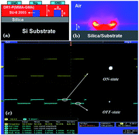
In this paper, a high-speed Mach–Zehnder interferometer type of electro-optic switch with coplanar waveguide electrodes was studied. The characteristic parameters of the switch were carefully designed and simulated. The fabrication was done by using standard semiconductor fabrication techniques such as spin-coating, photolithography, and wet etching. The device was fabricated based on electro-optic polymer-clad waveguides with the simple wet-etching procedure. The device shows a low insertion loss of about 7.3 dB. The measured switching rise time and fall time are 29.00 and 30.89 ns, respectively. This waveguide structure and the fabrication process are shown to be valuable for EO switches and modulators application.


1. Introduction

Advances in optical communication network systems over the past 10 years have been fueled by progress in laser and detector technology, as well as by the availability of high performance devices such as optical switches, optical modulators, optical attenuators and optical amplifiers.1–6 Optical switches are important elements in many applications, such as optical cross connect (OXC), optical add-drop multiplexing (OADM), and optical true time delay (TTD).7–9 Optical Mach–Zehnder interferometer (MZI) modulators and switches based on the EO effect have served as one of the fundamental and important elements in optical fiber data transmission system.10 Research is continuing to improve the performance of MZI devices such as driving voltage, bandwidth, response speed, and optical and microwave loss by means of new materials and novel structures.11–13 The parameters of EO MZI devices are determined by both the properties of EO materials and the electrode structures. Due to the physical properties of the EO materials and available processes, many techniques combining EO materials with structures have been used to improve the performance of the EO devices.14–16

Nonlinear optical (NLO) polymers for EO switches have attracted much interest because of their high EO coefficient, low dielectric constant, ultrafast frequency response, and low processing cost.17,18 Various organic chromophores and EO polymers have been studied for the application of EO devices.19–24 There are mainly two methods to incorporate the NLO chromophores into polymers: guest–host and side-chain or main-chain.25,26 Compared to the guest–host EO materials, in the side-chain or main-chain system, the chromophores are covalently linked to the polymers and the EO materials present higher EO coefficients and good thermal stability.

In addition to the EO characteristics of the materials, the performance of the optical MZI switches is also determined by the waveguide and electrode structures. Generally, a polymer EO waveguide consists of an EO core and transparent cladding layers. The EO core layer must be poled to induce a refractive index change under an applied voltage. Coplanar waveguide (CPW) electrodes and microstrip line (MSL) electrode are two main modulating electrode structures for EO modulators and switches.27,28 The MSL electrode has been mostly implemented in polymer modulators and switches because it can provide an excellent overlap between the modulating electric field and the optical mode. On the other hand, CPW switches have a smaller overlap with optical mode because the electrodes are on the surface of the waveguides. However for the typical optical MZI switch electrode spacing and width, the CPW electrodes have the advantage of lower microwave signal loss, which is a determining factor for the 3 dB bandwidth.10

In fact, the EO overlap factor is also relevant with the waveguide structure. In this paper, we will present an easy-to-fabricate approach to increasing the overlap in the CPW case by fabricating the EO polymer-clad waveguides on silica substrate. The switch structure consists of a waveguide core formed from an SU-8 polymer (commercially from MicroChem Corp.), and a cladding of P(MMA-GMA) side-chained with Disperse Red 1 (DR1, supplied by TCI Corp.) at 28% by weight. This work is based on all-wet etching method to provide high-quality waveguides and electrodes with low cost. The optical and thermal properties of the DR1-P(MMA-GMA) materials were characterized. Design procedures, simulation, fabrication, as well as performances of the EO switch were also described.

2. Waveguide material

In this work, cross-linkable polymer P(MMA-GMA) with chemical and physical stability properties was selected as the host material, which was synthesized by copolymerization of methylmethacrylate (MMA) and glycidyl methacrylate (GMA). The bisphenol-A epoxy was used as high-refractive index regulator. In the crosslinking approach, the guest material chromophores DR1 were covalently attached to the polymer as a side pendant of the main chain. Fig. 1 shows the chemical structure of the EO cladding material. The refractive index of cladding material could be easily controlled from 1.503 to 1.574 (@1550 nm) through regulating the weight percent of bisphenol-A epoxy and DR1.29,30 The refractive index of the EO polymer can be improved by increasing the proportion of DR1, and the EO coefficient is also improved. However, an excess of DR1 will led to the aggregation and increase the optical loss of the waveguide.30 Therefore, the concentration of DR1 was optimized to 28 wt%.
image file: c5ra11500k-f1.tif
Fig. 1 The chemical structures of (a) DR1-P(MMA-GMA) material and (b) bisphenol-A epoxy.

The DR1-P(MMA-GMA) films were prepared to measure the characteristics of thermal and EO coefficient. Thermal behavior of the EO cladding material was investigated by differential scanning calorimeter (DSC) and thermo-gravimetric analysis (TGA). The measured results were shown in Fig. 2. In the range from the room temperature to 125 °C, slight weight loss is seen, accompanied with endothermic behavior. Then a greatly intensity of weight loss was observed in the range from 125 to 270 °C. At the same time, there are two minor endothermic peaks around 125 and 190 °C, which can be related to the melt and release of the organic molecules. In next range of 270–420 °C, a large weight loss exists, accompanied with the largest exothermic peak which could be assigned to the decomposition and combustions of most of the organic materials. It reveals that the glass transition temperature of the core material is about 125 °C, and no decomposition was observed at around 270 °C. The EO coefficient γ33 of the 28 wt% dye concentration film was measured by the reflection method31 at a wavelength of 1310 nm, and was found to be 24.6 pm V−1. The long-term stability of the EO coefficient at room temperature was also characterized. After initial decay of about 10%, the γ33 remained stable at 22.2 pm V−1 for a test period of 1500 h. The absorbance of the core material SU-8 2005 was measured by Perkin Elmer Instruments UV-visible-near-IR λ19 spectrophotometer over a wavelength range of 300–2000 nm. Fig. 3 summarizes the results of the absorption measurements. The spectrum suggests that the SU-8 2005 polymer has a low absorption at 1310 nm and 1550 nm wavelength regions. Moreover, the root-mean-square (RMS) surface roughness of the film was only about 0.352 nm in 20 × 20 μm2 scan areas, which was measured by atomic force microscopy (AFM), and the 3D AFM image is shown in the inset of Fig. 3. This indicates that the film surface is smooth enough to provide a low scattering loss for the waveguide.


image file: c5ra11500k-f2.tif
Fig. 2 DSC and TGA of the EO cladding material.

image file: c5ra11500k-f3.tif
Fig. 3 Absorption spectrum of the core material as a function of wavelength. The inset shows the surface topology of the film measured by AFM.

3. Device design and simulation

The 1 × 1 polymeric MZI EO switch with CPW electrodes is shown schematically in Fig. 4(a). It consists of a symmetric Y-junction splitter which splits light into two decoupled waveguide arms, a phase tuning section with 18 mm-length in one of the waveguides, and a symmetric Y-junction coupler acting as the output combiner. The separation of the two waveguide arms was designed to be 50 μm and the angle of the Y-junction was designed to be 1° to get a low optical loss. As shown in Fig. 4(a), the applied electrical field can be induced with in a relative waveguide structure, accommodating the changes in refractive index profile, which, in turn, is used to realize the switching function. When there is no electrical field applied in the phase tuning arm, the phase difference of two light beam is 0, the switch is under ON-state. When the electrical field is applied in the phase tuning arm, the refractive index of the EO polymer will be changed due to Pockels effect. After propagating along the phase tuning arm, the phase difference between the two arms can be determined by
 
Δφ = (2πL/λne (1)
where L is the length of the phase tuning arm, λ is the operating wavelength. The change in effective refractive index for TM mode can be written as
 
image file: c5ra11500k-t1.tif(2)
where n is the refractive index of EO cladding, γ33 is the EO coefficient, V is the applied voltage in the phase tuning arm, G is the gap between the signal and ground electrodes, and Γ is the EO overlap integral factor between the applied electric field and optical mode32 and can be written as
 
image file: c5ra11500k-t2.tif(3)
where Ee is the electrical field and Eo is the optical field. After reaching the Y-junction coupler, the light beam from two MZI arms will interfere. When the phase difference of two light beam is π, the switch is under OFF-state. Then the related applied voltage, named the half-wave voltage, can be expressed as
 
image file: c5ra11500k-t3.tif(4)

image file: c5ra11500k-f4.tif
Fig. 4 (a) Schematic diagram and (b) cross-section view of AA′ in the EO region of the 1 × 1 polymeric EO switch; (c) the steady-state electrical field distribution in the activity waveguide cross-section.

The designed switch is based on polymer MZI structure fabricated on a SiO2 substrate. The cross-section view of AA′ in the EO section region is shown in Fig. 4(b), where a is the width and height of the core layer, and h is the thickness of the EO upper cladding. The core layer is SU-8 2005 material, which can be processed with wet-etching method. The upper cladding is the DR1-P(MMA-GMA) EO materials, which was synthesized in our lab. The modulating electrode is aluminum (Al) electrode.

The polymer waveguide usually consists of multiple layers, principally under cladding, core layer, and upper cladding. Their thickness, defined shape, and refractive index should be tailored carefully to provide single-mode confinement in the vertical and the lateral direction. Moreover, the defined shape of the core layer and the refractive index of the upper cladding have a significant effect on the optical field distribution. For the EO polymer-clad waveguide structure, the optical field should be optimized to the EO cladding layer to get a higher modulating efficiency. In the following simulation and discussion, the parameters are chosen as follows: free-space wavelength λ0 = 1550 nm, refractive index of core layer n1 = 1.568 and that of under cladding layer n2 = 1.450, respectively. The optical field distribution calculated by the beam propagation method (BPM) is displayed in Fig. 5. From Fig. 5(a), we can see that the confinement factor of the optical field in the EO cladding layer is increased with the refractive index increasing of EO material. However, the confinement factor of the optical field is decreased with the size increasing of the waveguide core, as shown in Fig. 5(b). Thus, the refractive index of the EO cladding material was tailored to be 1.532, and the size of the waveguide core was optimized to be 2.5 × 2.5 μm2.


image file: c5ra11500k-f5.tif
Fig. 5 (a) Relations between the optical mode in EO cladding and the refractive index of EO cladding; (b) relations between the optical mode in EO cladding and the size of core layer. The insets show the optical field distribution calculated by beam propagation method (BPM).

When the modulating voltage is supplied to the CPW electrodes, electrical field variation changes the effective index of the polymer waveguide mode due to the EO effect, and then changes the optical path length in the active waveguide. The induced phase shift in the active arm will affect the phase interference in the output combiner. The electrical field distribution was modeled using HFSS, which is a commercial finite element method (FEM) solver. The simulated electric field pattern in the activity waveguide cross-section is shown in Fig. 4(c). Depending on the phase change caused by external electrical field, the modulated output signals can be available.

4. Device fabrication, measurement and discussion

4.1 Fabrication

The EO polymer-clad waveguide switch was fabricated based on all-wet etching technique, including the waveguides and electrodes. The detailed fabrication process is as follows. Firstly, 2.5 μm-thick SU-8 2005 layer was spin-coated on a SiO2 substrate at a spinning rate of 7500 rpm for 20 s and pre-baked at 65 °C for 15 min, 90 °C for 20 min. Next, the coated wafer was exposed to UV light through a contact chromium mask for 8 s and post-baked at 65 °C for 15 min then 95 °C for 20 min. The UV light was generated from a mercury discharge lamp with peak intensity at a wavelength of 360 nm. After post-baking, the sample was developed for 35 s to form the waveguide cores, and then hard baked at 170 °C for 10 min. The hard bake is effective in controlling the refractive index and enhancing the chemical resistance. Finally, 5 μm-thick DR1-P(MMA-GMA) was spin-coated on the waveguide cores and baked at 120 °C for 3 h to form the EO upper cladding. The scanning electron microscope (SEM) images of the channel waveguide with/without upper cladding are shown in Fig. 6. After successfully fabricating the waveguides, 400 nm-thick Al layer was deposited on the EO polymer cladding by thermal evaporating. Then, photoresist BP212 was spin-coated on the Al film and baked at 80 °C for 20 min. The CPW electrodes were patterned using conventional photolithography and completed by a wet etching process. After fabricating the device, the chromophore alignment of EO core layer was achieved using the contact-poling method. The sample was purged with nitrogen (N2) at 110 °C for 30 min to remove the dissolved oxygen from the polymer. Then the sample was poled at 140 °C for 20 min in N2 atmosphere. The use of N2 atmosphere in the whole procedure is to prevent the oxygen-current-induced loss.
image file: c5ra11500k-f6.tif
Fig. 6 SEM images of the channel waveguide (a) without and (b) with upper cladding.

4.2 Switching performances

The fabricated EO switch was characterized for insertion loss and switching response in a dual drive setup with TM polarization at 1550 nm. The measuring process of the device is shown in Fig. 7(a). A light beam (at 1550 nm) generated by a tunable semiconductor laser (TSL-210, Santec) was directly coupled into the input port of the switch through a single mode fiber (SMF). The output light was detected using a germanium photodetector and measured by a power meter. Electrical signal was delivered to one arm of the interferometer via two microwave probes.
image file: c5ra11500k-f7.tif
Fig. 7 (a) The measuring process of the device; (b) the relative output pattern of the device without voltage applied; (c) the relative output pattern of the device with switching voltage applied.

For the optical measurement, the output light from the switch was firstly focused using a microscope objective lens, which images the output pattern, and captured by a charge-coupled device (CCD) camera. Then, the light beam was coupled directly into the optical power meter through a SMF to measure the insertion loss of the device. When no voltage was applied on the device, the maximum output power under ON-state was measured to be about −7.3 dBm (the relative output pattern is shown in Fig. 7(b)), which indicated that the fiber-to-fiber insertion loss of the tested sample with 3.1 cm-length was 7.3 dB, including the coupling loss, propagation loss, bending loss and the splitting loss. Whereas with switching voltage applied, the minimum output power under OFF-state was measured to be −19.8 dBm (the relative output pattern is shown in Fig. 7(c)), which indicated that the extinction ratio between ON- and OFF-states was 12.5 dB. At the same time, the propagation loss of the device was also measured by cut-back method. To increase the accuracy of the measurement, several waveguides were measured at each length. And the device had a propagation loss of about 1.02 dB cm−1 at 1550 nm wavelength. To measure the dynamic characteristics, a square-wave signal with 50 kHz was applied to the electrode with two microwave probes, and the output power was coupled into a photodiode detector through a SMF. The driving voltage of the switch and the detected optical response were simultaneously observed on an oscilloscope (4104B, Tektronix), as illustrated in Fig. 8. From Fig. 8, the upper trace is the square wave form of the switching voltage source, and the lower trace is the switching response from the device. The rise time and fall time are 29.00 and 30.89 ns, respectively.


image file: c5ra11500k-f8.tif
Fig. 8 Switching response of the device on a rectangular wave.

5. Conclusion

To develop polymer integrated waveguide devices in the optical communication system applications, a low loss polymeric optical switch with EO polymer-clad waveguide was designed and fabricated. The device was fabricated based on all-wet etching method with MZI structure. The DR1-P(MMA-GMA) material was successfully synthesized with relative high EO coefficient and good long-term stability. The characteristic parameters of the switch were carefully designed and simulated, and the fabrication was done using standard semiconductor fabrication techniques. At 1550 nm, measurements of the fabricated device demonstrated a low insertion loss of 7.3 dB and a fast response time (rise time and fall time are 29.00 and 30.89 ns, respectively). The reported switch with EO polymer-clad waveguide and easy fabrication process are suitable for planar active lightwave circuit applications.

Acknowledgements

This work was supported by the National Natural Science Foundation of China (Grant No. 61405070, 61475061, 61261130586, 61205032 and 61177027), China Postdoctoral Science Foundation funded project (No. 2015M571362), and the Science and Technology Development Plan of Jilin Province (No. 20140519006JH).

References

  1. N. Xie, T. Hashimoto and K. Utaka, IEEE Photonics Technol. Lett., 2009, 21, 1861–1863 CrossRef CAS .
  2. A. Densmore, S. Janz, R. Ma, J. H. Schmid, D.-X. Xu, A. Delâge, J. Lapointe, M. Vachon and P. Cheben, Opt. Express, 2009, 17, 10457–10465 CrossRef CAS .
  3. Y. Enami, D. Mathine, C. T. deRose, R. A. Norwood, J. Luo, A. K.-Y. Jen and N. Peyghambarian, Appl. Phys. Lett., 2009, 94, 213513 CrossRef PubMed .
  4. P. Song, L. Chen and Y. Chen, Opt. Express, 2012, 20, 6163–6169 CrossRef PubMed .
  5. D. Li, Y. Zhang, L. Liu and L. Xu, Opt. Express, 2006, 14, 6029–6034 CrossRef .
  6. M. A. Reilly, B. Coleman, E. Y. B. Pun, R. V. Penty, I. H. White, M. Ramon, R. Xia and D. D. C. Bradley, Appl. Phys. Lett., 2005, 87, 231116 CrossRef PubMed .
  7. G. Hu, B. Yun, Y. Ji and Y. Cui, Opt. Commun., 2010, 283, 2133–2135 CrossRef CAS PubMed .
  8. T. Segawa, S. Matsuo, T. Kakitsuka, Y. Shibata, T. Sato, Y. Kawaguchi, Y. Kondo and R. Takahashi, Opt. Express, 2010, 18, 4340–4345 CrossRef CAS PubMed .
  9. X. Wang, B. Howley, M. Y. Chen and R. T. Chen, Appl. Opt., 2007, 46, 379–383 CrossRef .
  10. R. Song, H.-C. Song, W. H. Steier and C. H. Cox, IEEE J. Quantum Electron., 2007, 43, 633–640 CrossRef .
  11. R. Song, A. Yick and W. H. Steier, Appl. Phys. Lett., 2007, 90, 191103 CrossRef PubMed .
  12. Y. Enami, B. Yuan, M. Tanaka, J. Luo and A. K.-Y. Jen, Appl. Phys. Lett., 2012, 101, 123509 CrossRef PubMed .
  13. R. Palmer, L. Alloatti, D. Korn, P. C. Schindler, M. Baier, J. Bolten, T. Wahlbrink, M. Waldow, R. Dinu, W. Freude, C. Koos and J. Leuthold, IEEE Photonics Technol. Lett., 2013, 25, 1226–1229 CrossRef CAS .
  14. Y. Enami, C. T. DeRose, D. Mathine, C. Loychik, C. Greenlee, R. A. Norwood, T. D. Kim, J. Luo, Y. Tian, A. K.-Y. Jen and N. Peyghambarian, Nat. Photonics, 2007, 1, 180–185 CrossRef PubMed .
  15. R. Ding, T. Baehr-Jones, Y. Liu, R. Bojko, J. Witzens, S. Huang, J. Luo, S. Benight, P. Sullivan, J.-M. Fedeli, M. Fournier, L. Dalton, A. Jen and M. Hochberg, Opt. Express, 2010, 18, 15618–15623 CrossRef CAS PubMed .
  16. S.-W. Ahn, W. H. Steier, Y.-H. Kuo, M.-C. Oh and H.-J. Lee, Opt. Lett., 2002, 27, 2109–2111 CrossRef CAS .
  17. A. L. Pyayt, Polymers, 2011, 3, 1591–1599 CrossRef CAS PubMed .
  18. H. Ma, B. Chen, T. Sassa, L. R. Dalton and A. K.-Y. Jen, J. Am. Chem. Soc., 2001, 123, 986–987 CrossRef CAS .
  19. J. Liu, G. Xu, F. Liu, I. Kityk, X. Liu and Z. Zhen, RSC Adv., 2015, 5, 15784–15794 RSC .
  20. Z. Li, W. Wu, Q. Li, G. Yu, L. Xiao, Y. Liu, C. Ye, J. Qin and Z. Li, Angew. Chem., Int. Ed., 2010, 49, 2763–2767 CrossRef CAS PubMed .
  21. J. Wu, H. Xiao, L. Qiu, Z. Zhen, X. Liu and S. Bo, RSC Adv., 2014, 4, 49737–49744 RSC .
  22. Z. Li, W. Wu, C. Ye, J. Qin and Z. Li, Polym. Chem., 2010, 1, 78–81 RSC .
  23. J. Wu, C. Peng, H. Xiao, S. Bo, L. Qiu, Z. Zhen and X. Liu, Dyes Pigm., 2014, 104, 15–23 CrossRef CAS PubMed .
  24. J. Wu, S. Bo, J. Liu, T. Zhou, H. Xiao, L. Qiu, Z. Zhen and X. Liu, Chem. Commun., 2012, 48, 9637–9639 RSC .
  25. Y.-H. Kuo, J. Luo, W. H. Steier and A. K.-Y. Jen, IEEE Photonics Technol. Lett., 2006, 18, 175–177 CrossRef CAS .
  26. G. A. Lindsay, A. J. Guenthner, M. E. Wright, M. Sanghadasa and P. R. Ashley, Polymer, 2007, 48, 6605–6616 CrossRef CAS PubMed .
  27. N. Dagli, IEEE Trans. Microwave Theory Tech., 1999, 47, 1151–1171 CrossRef CAS .
  28. M.-C. Oh, H. Zhang, C. Zhang, H. Erlig, Y. Chang, B. Tsap, D. Chang, A. Szep, W. H. Steier, H. R. Fetterman and L. R. Dalton, IEEE J. Sel. Top. Quantum Electron., 2001, 7, 826–835 CrossRef CAS .
  29. Z. Cao, L. Jin, X. Wang, Z. Cui and D. Zhang, Chem. Res. Chin. Univ., 2012, 28, 1091–1094 Search PubMed .
  30. J. Sun, X. Wang, J. Sun, X. Sun, C. Chen, F. Wang and D. Zhang, Mod. Phys. Lett. B, 2015, 29, 1550069 CrossRef CAS .
  31. C. C. Teng and H. T. Man, Appl. Phys. Lett., 1990, 56, 1734–1736 CrossRef CAS PubMed .
  32. R. Song and W. H. Steier, Appl. Phys. Lett., 2008, 92, 031103 CrossRef PubMed .

This journal is © The Royal Society of Chemistry 2015
Click here to see how this site uses Cookies. View our privacy policy here.