DOI:
10.1039/C5RA11392J
(Paper)
RSC Adv., 2015,
5, 78502-78507
Enhanced field emission properties of ZnO nanorods by surface modification
Received
15th June 2015
, Accepted 1st September 2015
First published on 1st September 2015
Abstract
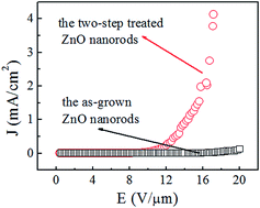
ZnO nanorods on Si substrates have been synthesized by a simple vapor phase transport method. A two-step surface modification, which involves coating with a very thin AlN layer followed by Ar+ plasma etching treatment, has been employed to enhance the field emission (FE) properties of ZnO nanorods. Compared with the FE properties of as-grown ZnO nanorods, the turn on field of the two-step surface modified ZnO nanorods decreased to 42% from 16.0 to 6.8 V μm−1 at the current density of 10 μA cm−2, and the FE current density increased by about 40 times, reaching as high as 4.1 mA cm−2 at an electric field of 17.4 V μm−1. It has been proposed that the enhancement in the field emission properties is due to the reduction of the effective work function and the low electron affinity of the thin AlN coating layer, as well as the enhanced local field near the reduced tips of the ZnO nanorods. This study provides an effective approach for enhancing the FE properties of semiconductor emitters.
1. Introduction
As a wide bandgap semiconductor, ZnO has attracted significant research interest due to its excellent physical and chemical properties, abundant nano-morphologies,1 and variety of applications.2–5 In particular, one-dimensional (1D) ZnO nanostructures, such as nanorods and nanowires, have been considered as candidates for field emission (FE) cathode materials6–10 because of the ease with which their morphology, dimensions and even spatial arrangement can be controlled, as well as because of their high thermal stability and oxidation resistance in harsh environments.11 However, compared with bulk materials, 1D nanostructured materials are relatively unstable and can be easily deformed during operation, especially under large current and high power density conditions.12 The operating voltages of the as-prepared ZnO for FE are generally high because of relatively high electron affinity (∼4.5 eV)13 and large work function (∼5.3 eV),14 which may limit its practical application. It is therefore essential to evaluate the FE performance of ZnO nanorods in detail.
In general, FE properties are evaluated by the classic Fowler–Nordheim (F–N) theory:6,15
|
 | (1) |
where
J is the current density,
E is the applied electric field,
ϕ is the work function of the emitter and
β is the field enhancement factor.
A and
B are constants with the values of 1.54 × 10
−6 (AV
−2 eV) and 6.83 × 10
9 (V eV
−3/2 m
−1), respectively. FE properties mainly depend on two essential parameters: the field enhancement factor and the work function of the emitter. Normally, the field enhancement factor is determined by the geometry, density and uniformity of the emitters and resistive potential drop across the nanostructure body. The work function of the emitter is independent of the geometry because it is a material related property. Accordingly, many efforts have been made to improve the FE properties of nanostructured materials such as modifying the morphology of the emitter, decreasing the work function through doping or coupling with other materials, and coating an ultrathin, low electron affinity semiconductor layer on the surface of the nanostructures. For example, Liao
et al.16 reported that ZnO nanowires coated with an α-CN
x film exhibited a turn-on field of 1.5 V μm
−1 at 10 μA cm
−2; Yuan
et al.11 deposited a HfN
x film on ZnO nanorod arrays and found that the turn-on field decreased from 6.60 to 2.42 V μm
−1 at 10 μA cm
−2. In comparison with the above mentioned α-CN
x and HfN
x, AlN shows great potential for use as cold cathode materials, due to its low (less than 1 eV), and sometimes negative, electron affinities.
17–20 Furthermore, thin film AlN layers can be easily prepared by the sputtering technique, and plasma etching is one of the effective ways to obtain a small tip radius for the emitters.
21,22 Therefore, two alternative approaches have been employed in this study to improve the FE properties of as-prepared ZnO nanorods: coating with an ultrathin AlN (low electron affinity semiconductor) layer to lower the effective work function of ZnO nanorods and Ar
+ plasma etching treatment to reduce the tip radius of ZnO nanorods. Furthermore, the combined effect of both tip-radius-dependence and AlN coating on the field emission performance of ZnO nanorods has been systematically studied.
2. Experimental
ZnO nanorods were grown on ZnO buffered silicon substrates through a simple vapor-phase transport process in a conventional horizontal tube furnace.23 In brief, mixed ZnO and graphite powder (molar ratio 1
:
1) was loaded into a quartz tube with one end closed, as a source material to prepare ZnO nanorods. The substrate was placed upstream in a small quartz tube. The small quartz tube was then transferred to a tube furnace. After being sealed, the system was pumped down and heated to 1000 °C within 100 minutes. The temperature of the substrate zone was set to about 650 °C, and the working pressure was kept at about 1600 Pa. The growth was maintained under a mixed flow of N2 (100 standard cubic centimeter per minute (sccm)) and O2 (2 sccm) for 20 minutes. Both ZnO buffer layers and AlN coating were prepared by the magnetron sputtering technique.
The morphology of the ZnO nanorods was characterized by field emission scanning electron microscopy (FESEM, Nova NanoSEM 430). The crystal structure and the composition of the AlN coated ZnO nanorods were analyzed by X-ray diffraction (XRD, X'pert PRO by PANalytical), transmission electron microscopy (TEM, FEI Tecnai G2 F30) and energy dispersive X-ray spectroscopy (EDS, Axis Ultra DLD). Field emission characterization was carried out in a diode configuration in a vacuum chamber with a base pressure of 1 × 10⁻⁵ Pa. Indium tin oxide (ITO) glass was used as the anode. The gap between the anode and sample surface was kept at 100 μm using a Teflon spacer. High voltage was supplied by a power source (Keithley 248), and the current was collected by an electrometer (Keithley 6485).
3. Results and discussion
After coating with AlN layers of various thicknesses, ZnO nanorods show similar surface morphology with the as-prepared ones. The thicknesses of the AlN coating layers were estimated to be about 3, 7, 13 and 20 nm by TEM. Selected SEM images of ZnO nanorods without and with AlN layers are shown in Fig. 1(a) and (b), respectively, where the thickness of the AlN coating is 7 nm. Clearly, quasi-aligned ZnO nanorods cover the entire substrate surface. No obvious difference in surface morphology can be observed for the ZnO nanorod samples before and after AlN coating. The diameters of the as-grown ZnO nanorods are in the range of 165–220 nm. Fig. 1(c) shows the corresponding XRD patterns of ZnO nanorods with and without AlN coating. Besides obvious wurtzite ZnO diffraction peaks of (002), (101) and (102) (JCPDS 36-1451), the AlN (100) peak (JCPDS 25-1133) is also observed for the AlN-coated ZnO nanorods. Fig. 1(d) shows the EDS spectrum of the ZnO nanorods after AlN coating; the elements Zn and O, N and Al were also detected in the sample. Both XRD and EDS results demonstrate the existence of AlN. Fig. 1(e) and (f) are the low and high magnification TEM images of a single ZnO nanorod with AlN coating, respectively. Clearly, the ZnO nanorod is wrapped with a thin AlN layer, and the thickness of the AlN is about 7 nm. Fig. 1(g) and (h) are the selected area electron diffraction (SAED) patterns of the ZnO nanorod and AlN thin film, respectively. The SAED pattern of the ZnO nanorod reveals that the ZnO nanorod is single crystalline with hexagonal wurtzite structure, and the AlN layer is poly-crystalline in nature.
 |
| Fig. 1 (a) and (b) SEM images of the as-prepared ZnO nanorods and ZnO nanorods with a 7 nm-AlN coating. (c) XRD patterns of ZnO nanorods. (d) EDS spectrum of ZnO nanorods coated with the AlN layer. (e) and (f) low and high magnification TEM images of a single ZnO nanorod coated with AlN. (g) and (h) SAED patterns of ZnO nanorods and the AlN layer, respectively. | |
The field emission properties of the ZnO nanorods with AlN coating were analyzed systematically. Fig. 2(a) shows the FE current density versus applied electric field (J–E) curves of ZnO nanorods coated with AlN layers. The thicknesses of the AlN layers are 0, 3, 7, 13 and 20 nm. It is noted that the turn-on (Eto) and threshold electric fields (Ethr) are defined as the E values required to produce current densities of 10 μA cm−2 and 1 mA cm−2, respectively. Without the AlN coating, the Eto of the ZnO nanorods is about 16.0 V μm−1 and the field emission current is about 0.13 mA cm−2 at the electric field of 20 V μm−1. Eto of the ZnO nanorods coated with a 3 nm-AlN layer is 14.2 V μm−1. When the thickness of the AlN layer increases to 7 nm, the Eto decreases to 9.2 V μm−1 and the FE current density dramatically increases to 1.80 mA cm−2 at the electric field of 20 V μm−1. However, Eto of the sample with the 20 nm-thick AlN layer barely changes, while its emission current drops abruptly to 0.66 mA cm−2 at the electric field of 20 V μm−1. Therefore, the AlN coating plays a significant role in the Eto of ZnO nanorods, and the optimum thickness of the AlN layer is about 7 nm in this study.
 |
| Fig. 2 Field emission properties of ZnO nanorods with and without AlN coating. (a) J–E curves and (b) the corresponding F–N plots. | |
The corresponding plots of ln(J/E2) versus 1/E of ZnO nanorods coated with AlN of various thicknesses are shown in Fig. 2(b). The slopes of the F–N plot are used to determine the field enhancement factor (β), which is estimated from the following equation:
|
 | (2) |
where
k is the slope. The field enhancement factor of the as-prepared ZnO nanorods was calculated to be 488, denoted as
β0, where
ϕ of ZnO is 5.3 eV. Assuming that the effect of the thin AlN coating on
β could be ignored because the thickness of the AlN layer is much smaller than the diameter of ZnO,
β values of the ZnO nanorods with thin AlN coating are always equal to
β0. Based on
eqn (2), the effective work functions (
ϕe) of ZnO nanorods with AlN coating layers were estimated and are presented in
Table 1. ZnO nanorods coated with thin AlN layers exhibit lower
Eto and higher FE current densities than the as-grown ZnO nanorods without AlN coating. On the basis of these results, it can be inferred that the AlN coating does enhance the field emission performance of ZnO nanorods. The bulk of electrons that come from the AlN layers coated on ZnO nanorods can escape easily from the emitter surface due to the low electron affinity of AlN, which in turn lowers the
Eto and increases FE current density. A more detailed mechanism of the enhanced FE properties will be discussed below.
Table 1 Summary of the FE turn-on fields, maximum current densities obtained at 20 V μm−1 and effective work functions of ZnO nanorods with and without AlN coatings
AlN thickness (nm) |
Turn-on field (V μm−1) |
Current density at electric field of 20 V μm−1 (mA cm−2) |
Effective work function, ϕ (eV) |
0 |
16.0 |
0.12 |
5.3 |
3 |
14.2 |
0.32 |
4.4 |
7 |
9.2 |
1.80 |
3.0 |
13 |
8.7 |
1.28 |
3.2 |
20 |
9.1 |
0.66 |
3.7 |
The enhancement factor β mainly depends on the radius of the tip of the emitters:24
|
 | (3) |
where
d is the spacing from the tip of the emitter to the anode plate,
r is the radius of the tip of the emitters and
s is the screening factor, which ranges from 0 (for densely arranged emitters) to 1 (for a single emitter). Clearly, at a constant
d spacing, reducing the tip radius of the emitters is another way to improve the field emission properties of ZnO nanorods.
21 Ar
+ plasma etching is considered to be a simple method for the nanostructure modulation.
Fig. 3 shows the SEM images of ZnO nanorods before and after Ar
+ plasma etching, and the insets show schematic diagrams of individual nanorods.
Fig. 3(a) shows the as-grown ZnO nanorods, having hexagonal top planes. The mean diameter of the ZnO nanorods is about 190 nm.
Fig. 3(b) and (c) are the SEM images of the ZnO nanorods etched by Ar
+ plasma for 4 and 20 min, respectively. Clearly, the top diameters of the ZnO nanorods are dramatically reduced. The mean diameters of the ZnO nanorods at the top are about 160 and 50 nm after 4 and 20 minutes of Ar
+ plasma etching, respectively.
 |
| Fig. 3 The SEM images of the as-prepared and plasma-etched ZnO nanorods; the insets show the schematic diagram of a single ZnO nanorod after plasma etching. (a) As-prepared ZnO nanorods; (b) plasma etching for 4 min; and (c) plasma etching for 20 min. | |
A more detailed study on the FE properties of ZnO nanorods before and after plasma etching was conducted. Fig. 4(a) shows the J–E curves of the ZnO nanorods before and after plasma treatment. Samples R0, R4 and R20 represent the pristine ZnO nanorods and as-prepared ZnO nanorods with top diameters of 160 and 50 nm, respectively. The Eto of sample R0 is 16.0 V μm−1 and the field emission current density reaches 0.12 mA cm−2 at an electric field of 20 V μm−1. With the reduction in the top diameter of the ZnO nanorods, the Eto of sample R4 is 9.5 V μm−1 and the emission current density is 0.84 mA cm−2 at the electric field of 20 V μm−1. With further reduction in the top-diameter of the ZnO nanorods to 50 nm, the Eto of sample R20 decreases abruptly to 4.8 V μm−1 and the emission current density increases to 1.96 mA cm−2 at the electric field of 20 V μm−1. Obviously, the Eto of the ZnO nanorods dramatically decreases and the field emission current greatly increases after plasma etching. Fig. 4(b) depicts the corresponding F–N plots. It should be noted that the F–N plots of samples R4 and R20 exhibit a nonlinear behavior over the entire range of the applied electric field. Each curve can be fitted by two straight lines of different slopes. The slope of the straight line in the high field region is larger than that in the low field region. In general, the nonlinear phenomenon seen in the F–N plot originates from the saturation of the conduction band current and the predominance of valence band current at high field values.25 Based on eqn (2), the β values of samples R4 and R20 were calculated to be 2382 and 4388 in the low field region, whereas 656 and 887 in the high field region, respectively. Clearly, the β values of samples R4 and R20 in the low field region are considerably larger than that of the as-grown ZnO nanorods, irrespective of low or high field region. The calculated relationship of the field enhancement factors is β0 < β4 < β20, which is consistent with the relationship of the emitter tip radius of r0 > r4 > r20. Similar nonlinear behavior has been observed for various ZnO nanostructures25,26 and other semiconductor materials.27
 |
| Fig. 4 (a) J–E curves of ZnO nanorods before and after plasma treatment; (b) the corresponding F–N plots. | |
The above mentioned alternative methods can improve the FE properties of ZnO nanorods to a certain extent. However, there is still a large room for the improvement of FE properties in ZnO nanorods with regards to the Eto and the emission current density. To further enhance the FE properties of ZnO nanorods, a two-step approach involving coating with a 7 nm-AlN thin film after plasma etching treatment for 20 min was employed. Fig. 5(a) shows the TEM image of the modified ZnO nanorods. The ZnO nanorods were thinned to about 50 nm at the tip and covered with a very thin AlN layer. Fig. 5(b) shows J–E curves of ZnO nanorods before and after the two-step treatment. It is noticed that the FE properties of the ZnO nanorods after the two-step treatment are enhanced significantly. The Eto and Ethr of the two-step treated ZnO nanorods are ∼6.8 and 12.8 V μm−1, respectively, which are considerably smaller than those of the samples discussed above. The corresponding current density reaches as high as 4.1 mA cm−2 at an electric field of 17.4 V μm−1, which is far larger than that of ZnO nanorods with the 7 nm-thick AlN layer coating and those subjected to Ar+ plasma treatment for 20 min. Fig. 5(c) is the F–N plot of the two-step treated ZnO nanorods. The field enhancement factor estimated from the slope is about 1700 (taking the effective work function of 3.0 eV, as evaluated in Table 1), which is nearly 3.5 times that of untreated ZnO nanorods. The stability of the field emission current of 1.3 mA cm−2 was also evaluated. Fig. 5(d) shows the current emission stability of ZnO nanorods after the two-step treatment. During the test period of 200 min, no obvious degradation of current was observed and the current fluctuation was less than 10% at the electric field of 15.0 V μm−1.
 |
| Fig. 5 (a) TEM image of ZnO nanorods after the two-step treatment, the inset is the magnified image of the ZnO nanorod tip; (b) J–E curves of the as-prepared ZnO nanorods and ZnO nanorods after the two-step treatment; (c) The F–N plots corresponding to J–E curves in (b); and (d) stability of emission current of ZnO nanorods after the two-step treatment. | |
It is well known that the surface states in a nanostructured semiconductor play an important role in its electron field emission properties.28 Schematic energy band diagrams for ZnO and AlN, ZnO nanorod emitters, and AlN/ZnO nanorod emitters are depicted in Fig. 6. The work function of n-type ZnO without heavy doping should lie between 4.2 and 5.8 eV, and the value for the intrinsic (undoped, n-type) ZnO is generally taken as 5.3 eV.29 For bare ZnO nanorods, electrons are emitted from the ZnO conduction band into a vacuum through the tunneling barrier, as shown in Fig. 6(b). A hetero-junction (semiconductor–semiconductor) is formed by AlN and ZnO after coating with a thin AlN layer. The work function of AlN (3.7 eV) being smaller than that of ZnO (5.3 eV) might enable the transfer of electrons from AlN to ZnO, but there is no effective emission of electrons from AlN without applying an electric field, due to its wide band gap. However, electrons injected from the junction induce a large band bending at the AlN/vacuum interface because of the field penetration in a high field,30,31 resulting in a lowering of the emission barrier; this leads to the reduction of the effective work function [Fig. 6(c)]. Therefore, a thin AlN layer on the ZnO nanorods lowers the effective work function of the ZnO nanorods, which in turn enhances the FE performance. In this case, electron emission occurs as follows: (1) the electrons are injected through the interface from ZnO into AlN, (2) followed by transportation in the AlN thin film, and (3) emission from the AlN surface. It is clear that the electrons are emitted into the vacuum more easily from the AlN surface due to the lower affinity of AlN. Moreover, the FE characteristics are evidently modulated by varying the thickness of the coating layer.31,32 In this study, the optimum thickness is around 7 nm, which is among those stated in other reports.20,32
 |
| Fig. 6 Schematic energy band diagram for (a) ZnO and AlN, (b) bare ZnO nanorod emitters and (c) AlN/ZnO nanorod emitters. | |
4. Conclusions
In summary, a two-step surface modification involving coating with a thin AlN layer after reducing the tip radius of emitters by plasma etching treatment was adopted to enhance the field emission of ZnO nanorods. Compared with as-grown ZnO nanorods, the turn-on field of the two-step surface modified ZnO nanorods was reduced to 42%, and the FE current density was enhanced about 40 times, reaching as high as 4.1 mA cm−2 at an electric field of 17.4 V μm−1. The characteristics of the enhanced FE properties of ZnO nanorods in this study demonstrate an effective and simple way to improve the field emission properties of nanorods with large top diameters.
Acknowledgements
This study is supported by the National Natural Science Foundation of China (No. 51102098)
References
- A. B. Djurisic, A. M. C. Ng and X. Y. Chen, Prog. Quantum Electron., 2010, 34, 191–251 CrossRef CAS PubMed.
- Ü. Özgür, Ya. I. Alivov, C. Liu, A. Teke, M. A. Reshchikov, S. Doğan, V. Avrutin, S.-J. Cho and H. Morkoç, J. Appl. Phys., 2005, 98, 041301 CrossRef PubMed.
- T. S. Herng, A. Kumar, C. S. Ong, Y. P. Feng, Y. H. Lu, K. Y. Zeng and J. Ding, Sci. Rep., 2012, 2, 587 CAS.
- J. L. Gomez and O. Tigli, J. Mater. Sci., 2013, 48, 612–624 CrossRef CAS.
- A. B. Djurišić, X. Chen, Y. H. Leung and A. M. C. Ng, J. Mater. Chem., 2012, 22, 6526–6535 RSC.
- N. Pan, H. Z. Xue, M. H. Yu, X. F. Cui, X. P. Wang, J. G. Hou, J. X. Huang and S. Z. Deng, Nanotechnology, 2010, 21, 225707 CrossRef PubMed.
- C. X. Xu and X. W. Sun, Appl. Phys. Lett., 2003, 83, 3806–3808 CrossRef CAS PubMed.
- C. Geng, Y. Jiang, Y. Yao, X. Meng, J. A. Zapien, C. S. Lee, Y. Lifshitz and S. T. Lee, Adv. Funct. Mater., 2004, 14, 589–594 CrossRef CAS PubMed.
- Y. C. Chang, RSC Adv., 2014, 4, 56241–56247 RSC.
- C. L. Liu, H. Gao, L. Li, X. Liu, Q. Gao, H. X. Cuo, T. T. Chen and G. Q. Miao, RSC Adv., 2013, 3, 26149–26152 RSC.
- L. Yuan, G. Fang, C. Li, J. Li, M. Wang, N. Liu and X. Zhao, Surf. Coat. Technol., 2008, 202, 3480–3484 CrossRef CAS PubMed.
- Z. W. Song, R. Z. Wang, W. Zhao, B. Wang and H. Yan, J. Phys. Chem. C, 2012, 116, 1780–1783 CAS.
- Z. L. Wang and J. Song, Science, 2006, 312, 242–246 CrossRef CAS PubMed.
- C. J. Lee, T. J. Lee, S. C. Lyu, Y. Zhang, H. Ruh and H. J. Lee, Appl. Phys. Lett., 2002, 81, 3648–3650 CrossRef CAS PubMed.
- F. Chen, X. H. Ji and Q. Y. Zhang, Carbon, 2015, 81, 124–131 CrossRef CAS PubMed.
- L. Liao, J. C. Li, D. F. Wang, C. Liu, C. S. Liu, Q. Fu and L. X. Fan, Nanotechnology, 2005, 16, 985–989 CrossRef.
- M. C. Benjamin, C. Wang, R. F. Davis and R. J. Nemanich, Appl. Phys. Lett., 1994, 64, 3288–3290 CrossRef CAS PubMed.
- S. C. Shi, C. F. Chen, S. Chattopadhyay, Z. H. Lan, K. H. Chen and L. C. Chen, Adv. Funct. Mater., 2005, 15, 781–786 CrossRef CAS PubMed.
- Y. Tang, H. Cong, Z. Chen and H. Cheng, Appl. Phys. Lett., 2005, 86, 233104–233113 CrossRef PubMed.
- Y. J. Kim, J. Cho, Y. J. Hong, J. M. Jeon, M. Kim, C. Liu and G. C. Yi, Nanotechnology, 2010, 21, 055303 CrossRef PubMed.
- Y. W. Zhu, A. M. Moo, T. Yu, X. J. Xu, X. Y. Gao, Y. J. Liu, C. T. Lim, Z. X. Shen, C. K. Ong, A. T. S. Wee, J. T. L. Thong and C. H. Sow, Chem. Phys. Lett., 2006, 419, 458–463 CrossRef CAS PubMed.
- C. Li, G. Fang, L. Yuan, N. Liu, J. Li, D. Li and X. Zhao, Appl. Surf. Sci., 2007, 253, 8478–8482 CrossRef CAS PubMed.
- Z. X. Ye, X. H. Ji and Q. Y. Zhang, J. Mater. Sci.: Mater. Electron., 2015, 26, 5232–5236 CrossRef CAS.
- V. Filip, D. Nicolaescu, M. Tanemura and F. Okuyama, Ultramicroscopy, 2001, 89, 39–49 CrossRef CAS.
- A. A. Al-Tabbakh, M. A. More, D. S. Joag, I. S. Mulla and V. K. Pillai, ACS Nano, 2010, 4, 5585–5590 CrossRef CAS PubMed.
- N. S. Ramgir, I. S. Mulla, K. Vijayamohanan, D. J. Late, A. B. Bhise, M. A. More and D. S. Joag, Appl. Phys. Lett., 2006, 88, 042107–42113 CrossRef PubMed.
- J. Chen, S. Z. Deng, J. C. She, N. S. Xu, W. Zhang, X. Wen and S. Yang, J. Appl. Phys., 2003, 93, 1774–1777 CrossRef CAS PubMed.
- S. S. Warule, N. S. Chaudhari, B. B. Kale, K. R. Patil, P. M. Koinkar, M. A. More and R.-i. Murakami, J. Mater. Chem., 2012, 22, 8887–8895 RSC.
- Y. Xu and M. A. A. Schoonen, Am. Mineral., 2000, 85, 543 CAS.
- R. Z. Wang, B. Wang, H. Wang, H. Zhou, A. P. Huang, M. K. Zhu, H. Yan and X. H. Yan, Appl. Phys. Lett., 2002, 81, 2782–2784 CrossRef CAS PubMed.
- V. T. Binh and C. Adessi, Phys. Rev. Lett., 2000, 85, 864–867 CrossRef CAS.
- Z. Q. Duan, R. Z. Wang, R. Y. Yuan, W. Yang, B. Wang and H. Yan, J. Phys. D: Appl. Phys., 2007, 40, 5828–5832 CrossRef CAS.
|
This journal is © The Royal Society of Chemistry 2015 |
Click here to see how this site uses Cookies. View our privacy policy here.