
Structural, optical and electronic properties of homoepitaxial GaN nanowalls grown on GaN template by laser molecular beam epitaxy
S. S. Kushvaha*a,
M. Senthil Kumara,
A. K. Shuklaa,
B. S. Yadavb,
Dilip K. Singha,
M. Jewariyaa,
S. R. Ragama and
K. K. Mauryaa
aCSIR-National Physical Laboratory, Dr. K. S. Krishnan Road, New Delhi-110012, India. E-mail: kushvahas@nplindia.org
bSolid State Physics Laboratory, Timarpur, Lucknow Road, Delhi-110054, India
First published on 12th October 2015
Abstract
We have grown homoepitaxial GaN nanowall networks on GaN template using an ultra-high vacuum laser assisted molecular beam epitaxy system by ablating solid GaN target under a constant r.f. nitrogen plasma ambient. The effect of laser repetition rate in the range of 10 to 30 Hz on the structural properties of the GaN nanostructures has been studied using high resolution X-ray diffraction, field emission scanning electron microscopy and Raman spectroscopy. The variation of the laser repetition rate affected the tip width and pore size of the nanowall networks. The z-profile Raman spectroscopy measurements revealed the GaN nanowall network retained the same strain present in the GaN template. The optical properties of these GaN nanowall networks have been studied using photoluminescence and ultrafast spectroscopy and an enhancement of optical band gap has been observed for the nanowalls having a tip width of 10–15 nm due to the quantum carrier confinement effect at the wall edges. The electronic structure of the GaN nanowall networks has been studied using X-ray photoemission spectroscopy and it has been compared to the GaN template. The calculated Ga/N ratio is largest (∼2) for the GaN nanowall network grown at 30 Hz. Surface band bending decreases for the nanowall network with the lowest tip width. The homoepitaxial growth of porous GaN nanowall networks holds promise for the design of nitride based sensor devices.
1. Introduction
The III-nitride semiconductors have many potential applications in the field of optoelectronic devices such as laser diodes (LDs), light emitting diodes (LEDs) and solar cells among others.1–5 Among the III-nitrides, GaN has received enormous attention because its energy band gap can be largely tuned from the infra-red to deep ultraviolet region by alloying it with In and Al metals. The GaN film is also being used as a base layer for the fabrication of nitride based heterostructures and devices because the band gap of GaN (3.4 eV) lies in between InN (0.7 eV) and AlN (6.2 eV).6,7 Apart from flat and smooth GaN thin films,8,9 various GaN nanostructures such as nanowires, nanotubes, nanowalls, nanorods etc. have been grown on a variety of substrates using different growth techniques for various applications.10–17 In spite of the promising physical and electrical properties of the GaN nanowires, nanorods and nanotubes, it is quite complicated to separate them individually in self-assembly for specific applications. On the other hand, nanowalls are drawing special attention due to continuity in the lateral direction and porous surfaces for fruitful applications in the field of nitride based sensor technology and nano-devices.15,18–22Recently, a few research groups have reported the growth of GaN nanowall networks on sapphire18,21 and Si(111)19,20 using plasma assisted molecular beam epitaxy (PA-MBE). Most of the GaN nanowall networks have been grown heteroepitaxially on these substrates under extremely high N to Ga flux ratio conditions. Kesaria et al.18,22 reported that the spontaneous growth of GaN nanowall honeycomb network on sapphire (∼14% lattice mismatch) is due to the presence of misfit dislocations as nucleation centers on sapphire substrates. The difference in lattice constants, thermal expansion coefficients and electrical properties of the substrate and overlayer in heteroepitaxial growth can cause external biaxial strain in the GaN films. It has been suggested that strain due to lattice mismatch is a very important factor for occurrence of GaN nanowall network growth.18,22 However, it would be interesting to study if GaN nanowall can also form on lattice-matched substrate. There are a few reports on the growth of ZnO nanowall networks on closely lattice-matched GaN template (lattice mismatch ∼1.8%) with and without presence of metal catalyst using metal organic chemical vapor deposition (MOCVD).23–26 Recently, Poppitz et al.15 have grown GaN nanowall networks on SiC (lattice mismatch ∼3.5%) using ion-beam assisted MBE. However, the homoepitaxial growth of GaN nanowall networks on thick GaN epilayer grown on sapphire (0001), commonly referred as a GaN template, has not been reported.
Here, we report the homoepitaxial growth of GaN nanowall networks on MOCVD grown GaN template using a laser assisted MBE (LMBE) (also known as ultra-high vacuum pulsed laser deposition or UHV-PLD) system. Recently, LMBE has emerged as a powerful technique to grow high quality GaN layers at relatively lower temperatures on various substrates.9,27–30 The nanowalls have been grown by laser ablation of a hydride vapor phase epitaxy (HVPE) grown high purity polycrystalline GaN solid target in the presence of r.f. nitrogen plasma. A higher growth rate is found to be favorable for the homoepitaxial formation of GaN nanowall with tip width <15 nm. An enhanced optical band gap is obtained due to carrier confinement. The photoluminescence (PL) spectroscopy showed the direct evidence of the blue shift in near band edge (NBE) peak for the GaN nanowalls width <10–15 nm keeping the template NBE peak position unchanged. We have used X-ray photoemission spectroscopy (XPS) to understand the electronic structure as well as chemical composition of GaN nanowall network and it has been compared to GaN template. Binding energy shift of core level (Ga 3d and N 1s) spectra, high Ga/N ratio and change in VB maxima position for lowest tip width GaN nanowall network provides the evidence of N vacancy related defect states.
2. Experimental details
2.1. Growth of GaN nanowalls using LMBE
The GaN nanowalls were grown on MOCVD deposited 3.5 μm thick GaN templates on sapphire (0001) substrates in a LMBE system (SVTA, USA) equipped with r.f. nitrogen plasma source, reflection high energy electron diffraction (RHEED; Staib Instrument, Germany) and multiple laser ablation targets. The base pressure of growth chamber is <2 × 10⁻¹⁰ Torr. A high purity HVPE grown polycrystalline solid GaN target (99.9999%) was ablated using a KrF excimer laser (wavelength: 248 nm, pulse: 25 ns) with a laser energy density of ∼2.5 J cm−2 at various laser repetition rates, such as 10, 20 and 30 Hz. GaN templates of dimension 10 mm × 10 mm were diced from a 2 inch diameter MOCVD GaN epilayer (LUMILOG) grown on sapphire (0001). Surface defects and other physical properties of the template are assumed to be same for all growth as they were diced from a single GaN template wafer. All the GaN samples were grown at a fixed substrate temperature of 700 °C for 2 h with 2 rpm clock wise rotation of the substrate and anti-clock wise spinning of the target. Growth was performed in a constant nitrogen (N) plasma environment using semiconductor grade nitrogen gas with a flow rate of ∼0.35 sccm and an r.f. forward power of 250 W. The growth of GaN nanostructures was monitored by in situ RHEED. The thickness of LMBE grown GaN films on template are measured using a stylus profilometer as about 150, 220 and 300 nm for 10, 20 and 30 Hz laser repetition rates, respectively. The field emission scanning electron microscopy (FESEM) morphology, high resolution X-ray diffraction (HR-XRD) rocking curve FWHM and PL data obtained at different locations of 10 mm × 10 mm samples are very similar which indicate that the LMBE grown GaN nanowalls are quite uniform over this area.2.2. Characterization techniques
Structural properties of the LMBE grown GaN nanostructures have been investigated using HR-XRD, FESEM and Raman spectroscopy. X-ray rocking curves (XRC) of (0002) and (10–12) diffraction planes were measured by a PANalytical HR-XRD system using CuKα1 source to determine the crystalline quality of the GaN films. The plane and 45° tilt view images of the GaN nanowall networks were obtained using a FE-SEM (FIB, ZEISS, Germany) operated at 5 kV. Raman spectra were recorded using a 514 nm excitation light from Ar+ laser and a micro-Raman spectrometer with 50× objective lens (Renishaw inVia Raman Microscope system). The z-profile of the Raman spectrum was recorded using piezo-electric controlled movement of sample stage along the incident beam direction. Scattered light from the sample was collected in the backscattering geometry.Optical properties of the samples have been studied with commercial PL system using a 266 nm continuous-wave solid state ultra-violet laser as an excitation source. Ultrafast spectroscopy measurements on the GaN samples have been performed using a Ti:sapphire laser (35 fs, 4 mJ per pulse, 1 kHz, 800 nm). The laser beam is split into two: one with high intensity as a pump (330 nm) and the other with a weak intensity as a probe (560 nm). The probe beam is optically delayed with respect to pump beam using a computer controlled delay stage. The intrinsic temporal resolution of delay stage is 7 fs. The time resolved study was performed using HELIOS spectrometer (Ultrafast Systems). Here we have performed ultrafast pump-probe spectroscopy of GaN samples using 330 nm as a pump beam (power ∼25 mW) at normal incidence and the change in absorption was detected by using a gated CMOS detector.
Ex situ XPS measurements were carried out in an UHV Multi Probe Surface Analysis System (MPSAS) with a base pressure of 4 × 10⁻¹¹ Torr from Omicron Nanotechnology GmbH. The chamber is equipped with an EA 125 electron energy analyzer, monochromatic Al Kα and non-monochromatic dual anode (Al Kα and Mg Kα) X-ray sources. Samples were mounted with UHV compatible conducting carbon tape. An electrical contact was established between the sample surface and grounded sample plate with a highly conducting UHV compatible Ag paint in order to minimize charging during the XPS measurements. This procedure helped us to avoid any significant time dependent charging. However, finite and time dependent charging was still observed and it was corrected using C 1s (284.8 eV) core-level binding energy (BE). C 1s core levels were measured throughout the experiment particularly, before and after each XPS spectra to correct any small shift due to charging. All binding energies have been referenced to the Fermi edge of an Ar+ sputtered clean polycrystalline Ag sample. Uncertainty in determining the BE position and full width at half maximum (FWHM) is estimated to be ±0.05 eV. Most of the XPS data shown here, unless specifically mentioned, has been acquired using monochromatic Al Kα X-ray source. All the core level and valence band (VB) spectra were acquired using 20 eV analyzer pass energy. Overall experimental energy resolution with monochromatic Al Kα (1486.7 eV) and non-monochromatic Mg Kα (1253.5 eV) is 0.45 and 0.9 eV, respectively. All the spectra reported here were obtained at an emission angle of 40°. Photoemission angle has been defined with respect to sample surface parallel. Mixtures of Gaussian and Lorentzian (largely Gaussian) peaks have been used to fit the core level and VB spectra. Shirley method has been used to remove secondary electron background.31
3. Results and discussion
3.1. Structural properties of LMBE grown homoepitaxial GaN nanostructures
The LMBE growth of GaN layers was monitored by in situ RHEED and the typical RHEED pattern obtained for the GaN template and the LMBE grown GaN sample along [11–20] and [10–10] directions have been presented in Fig. 1(a and b). The GaN template exhibited a streaky RHEED pattern [Fig. 1(a)] indicating the smooth surface but the pattern changed to spotty once the LMBE growth of GaN was commenced [Fig. 1(b)]. In plasma assisted MBE growth of GaN, it has been well established that the Ga-rich flux condition promotes two-dimensional (2D) growth while N-rich condition assists 3D growth mode. And therefore, in situ RHEED is used as a potential tool to monitor the N/Ga flux ratio on the GaN growth front.27,32 The spotty RHEED pattern of LMBE grown GaN film indicated that the GaN grows homoepitaxially on the template in 3D mode under N-rich (N/Ga > 1) growth condition.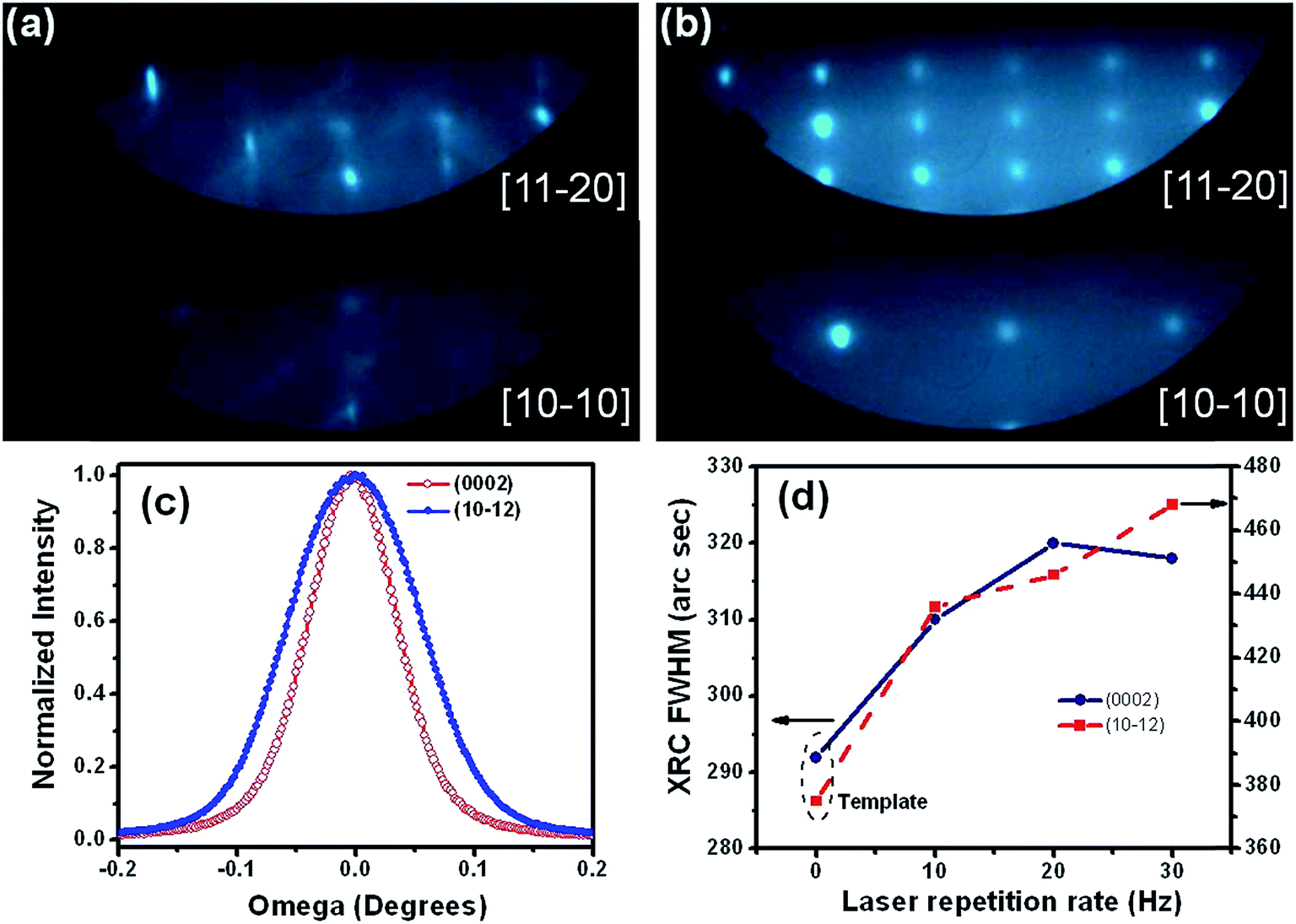 | ||
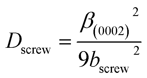
| Fig. 1 A typical RHEED pattern taken along [11–20] and [10–10] directions of: (a) GaN template and (b) LMBE grown GaN. (c) A typical normalized XRC of GaN (0002) and (10–12) planes of LMBE grown (30 Hz) GaN on template. (d) XRC FWHM values of GaN (0002) and (10–12) planes with respect to laser repetition rate. | ||
Furthermore, the crystalline quality of the GaN samples was characterized by XRC measurements of GaN (0002) and (10–12) planes and the typical spectra are presented in Fig. 1(c). From XRC measurements, it is found that the XRC FWHM values of the LMBE grown GaN samples for (0002) plane are almost similar (310–320 arc second) as that of the template (292 arc second) [Fig. 1(d)]. However, the FWHM values of GaN (10–12) plane increased with increasing the laser repetition rate from 10 (436 arc second) to 30 Hz (468 arc second) compared to the GaN template (375 arc second). We have estimated the total dislocation density (Dtotal) present in LMBE grown GaN layers on template at different laser repetition rates using the following equations:33,34
 | (1) |
 | (2) |
| Dtotal = Dscrew + Dedge | (3) |
The surface morphology of the LMBE grown GaN nanostructures were characterized by FESEM. Fig. 2(a and b) shows top-view and 45° tilted FESEM images of the GaN film grown on template with the laser repetition rate of 10 Hz. Top view image [Fig. 2(a)] shows the growth of a dense, un-coalesced GaN film. The RHEED measurements also revealed that the growth of GaN on template is three-dimensional (3D). However, 45° tilt FESEM image [Fig. 2(b)] shows the GaN nanowall network-like feature with pore size ∼40–70 nm. With further increase in the repetition rate to 20 Hz, the formation of GaN nanowall network structure has been clearly observed as shown in Fig. 2(c and d). It has a large number of hexagonal-shaped pores of size ranging from 90–120 nm with the nanowall tip width of about 20–30 nm. The pore size of the GaN nanowall network increased with increasing laser repetition rate to 30 Hz as clearly seen in Fig. 2(e and f). The size of the nanowalls grown at 30 Hz has been statistically analyzed and it is found that the tip width of nanowalls is about 10–15 nm and the pore size of the nanowall network increased to be 120–180 nm. Increase of pore size of the nanowall network grown at higher repetition rate can be related to low surface diffusion and kinetic energy of GaN adatoms or clusters due to increased flux rate.
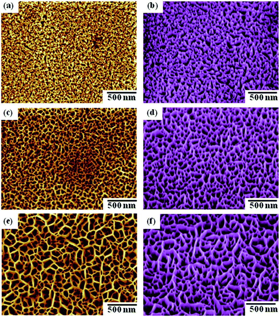 | ||
| Fig. 2 Plan and 45° tilt view FESEM images of the GaN surface grown on GaN template at various laser repetition rates: (a and b) 10 Hz, (c and d) 20 Hz, (e and f) 30 Hz. | ||
The growth of GaN nanowall network on different substrates using MBE occurs when N to Ga flux ratio is high.18–22 The N to Ga ratio also determines the width of the nanowalls as reported previously.19 For example, the narrow width nanowalls (∼30 nm) have been grown on Si(111) with a N to Ga ratio of 980 while film with flat surface is obtained when N to Ga ration is 180.19 In case of porous GaN nanowall networks grown on SiC using ion beam assisted MBE at different substrate temperatures (750 and 850 °C), the N ion to Ga atom ratio is reported to be between 2.7 and 6.3.15 Thus, in MBE GaN growth, the N to Ga flux ratio determines the growth mode and the structure of GaN films. For example, a 2D growth mode occurs when Ga flux is excess whereas N-rich growth condition promotes a 3D or island growth mode.32,35 In our study, N to Ga ratio will be more than one as the growth of GaN nanowall network occurs on GaN template by ablation of solid GaN target in the presence of additional supply of r.f. nitrogen plasma. Our in situ RHEED observations also support the N-rich LMBE growth of GaN on template.
Although detailed theoretical and simulation studies are required for deep understanding of the growth mechanism of GaN nanowalls, a possible growth mechanism can be proposed based on the present and previous experimental studies on growth of GaN nanowall. The reports unanimously suggest that N-rich growth condition is the most important parameter for GaN nanowall formation. The growth mechanism for GaN nanowalls also depends on the type of the substrate used. GaN nanowalls were grown on sapphire (lattice mismatch ∼14%) and Si(111) (lattice mismatch ∼16%) substrates using MBE technique in extremely N-rich condition and the growth process has been explained on the basis of large lattice mismatch, the misfit dislocation and strain.18–22 For GaN nanowalls grown on SiC substrate (lattice mismatch ∼3.5%) using ion beam assisted MBE, the growth process was explained on the basis of N-rich growth conditions in combination with high growth temperature and the energetic N ion irradiation during the growth.15 For homoepitaxial growth of GaN nanowalls on GaN template, the effect of strain will be minimal. Hence, the growth mechanism of LMBE grown homoepitaxial GaN nanowall network can be understood on the basis of N-rich growth condition and high flux rates at the growth temperature of 700 °C. In this work, we employed laser ablation of a HVPE grown GaN bulk target under the RF activated nitrogen plasma ambient to grow GaN, which is clearly N-rich flux condition prone for 3D growth. When the repetition rate is low (10 Hz, low flux rate), mostly coalesced but rough surface GaN film is obtained due to the enough time available for adatom diffusion at the growth surface before the next impinging GaN flux. In case of high laser repetition rate >10 Hz (higher flux rate), the full coalescence of GaN islands can be inhibited as the increased impinging rate of GaN flux will effectively reduce the surface mobility of adatoms. As a result, limited lateral growth will take place at higher repetition rates favoring the growth at vertical direction that will eventually decrease the wall thickness and increase the pore size of the GaN nanowall network. In addition, the relatively higher sticking coefficient of Ga at (0001) plane compared to other planes will further contribute for the vertical growth.22,36 From our results, it is evident that GaN nanowalls could be grown homoepitaxially on GaN template under N-rich condition but at higher flux rates.
To examine the strain status in our films, we have performed the z-profile Raman spectroscopy with monotonically varying depth of focus by movement of objective lens normal to the sample surface. Fig. 3(a) shows the z-profile Raman spectra of GaN film grown on template at 10 Hz. The direction of arrow indicates spectra recorded sequentially with decreasing distance between sample and objective lens. With decreasing separation between sample and objective lens, scattered signal was collected sequentially from top LMBE grown GaN to MOCVD grown GaN template and finally to sapphire (0001) substrate. For wurtzite GaN films, the Raman scattering phonon modes are A1(LO), A1(TO), E1(LO), E1(TO) and E2(high) in which E1(TO) peak attribute mainly due to the presence of dislocations or defects in GaN film.37 The Raman selection rules for GaN (0001) shows that the A1(LO) and E2(high) phonon modes are expected to be more pronounced in the backscattering geometry. The line shape, FWHM value and shift in E2(high) peak describes the crystalline quality and the stress/strain present in the GaN films, whereas A1(LO) peak determines the carrier concentration density and electron mobility.38,39 Since, the wide band gap of GaN renders it optically transparent, the depth of laser focus is ensured by monitoring the maximum intensity of E2(high) mode of GaN by increasing the separation between objective lens and sample. It ensures that signal is recorded from the top LMBE grown GaN layer. As the z-separation between the sample and the objective lens decreases E2(high) mode (571.3 cm−1) intensity begins to fall and a new peak starts to appear at 576.8 cm−1 from sapphire.40 Similarly, the A1(LO) mode at 736.8 cm−1 disappears and a new peak is observed at 751 cm−1 corresponding to sapphire.40 The z-scan Raman measurements enabled us to distinguish between signals coming from the top surface of LMBE grown GaN towards substrate, distinctly. Similar results were obtained for the samples grown at 20 and 30 Hz, as well.
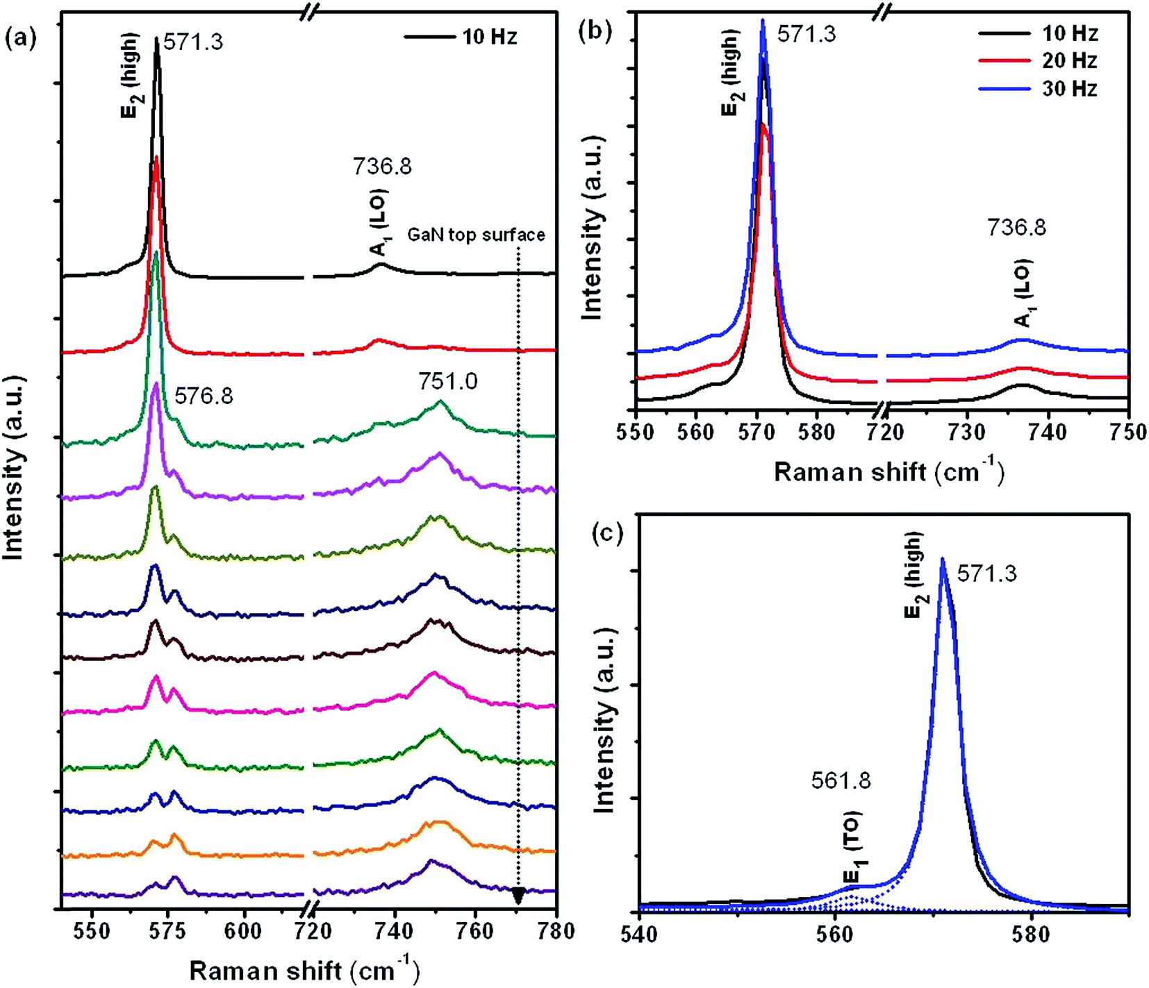 | ||
| Fig. 3 (a) The z-profile Raman spectra with monotonically varying depth of focus from top layer LMBE GaN towards the substrate grown at 10 Hz. (b) Raman spectra showing the E2(high) and A1(LO) modes for the LMBE grown GaN at laser repetition rates 10, 20 and 30 Hz. (c) Typical fitted Raman spectrum for E2(high) and E1(TO) for estimating FWHM values. | ||
Fig. 3(b) shows the Raman spectra of LMBE GaN nanowalls grown at the laser repetition rates of 10, 20 and 30 Hz. All the samples exhibit a peak around 571.1–571.4 cm−1 [E2(high)] and 736.8 cm−1 [A1(LO)]. For comparison of spectral line profiles of three samples, E2(high) mode was fitted with Lorentzian line shape as shown in Fig. 3(c) for the 10 Hz grown LMBE GaN film. The peak position, FWHM values of GaN Raman peaks for all samples is enlisted in Table 1. Before LMBE GaN growth, the Raman spectra of bare MOCVD grown GaN template consists of GaN E2(high) peak at 571.1 cm−1 and A1(LO) mode at 736.9 cm−1. Our obtained E2(high) peak position at 571.1 cm−1 is similar to the previous reported E2(high) Raman mode (572 cm−1) for (3 μm thick GaN on sapphire) GaN template.41 Compared with stress-free thick GaN Raman E2(high) peak position (567.6 cm−1),42 GaN template possesses intrinsic compressive stress.43 However, in case of LMBE grown GaN films on template, we found that the LMBE grown GaN films exhibit almost exactly same peak position for E2(high) mode as of template as given in Table 1. Our Raman spectroscopy measurements reveal that even though there is intrinsic strain present in the template,43 there is no additional strain in LMBE grown GaN nanowall networks with respect to the GaN template/substrate. These samples possess a similar order of crystallinity as indicated by the FWHM of Raman and HR-XRD peaks. The 736.8 cm−1 peak is assigned to A1(LO) mode of GaN. Analogous to E2 peak, the peak position and FWHM of A1(LO) mode is same for all the three samples. There is a shoulder peak near E2(high) mode at 561.8 cm−1 for 10 Hz, which is assigned to E1(TO) mode. The E1(TO) mode observed at 562.2 cm−1 for 20 Hz and at 561.3 cm−1 for 30 Hz. The peak width of E1(TO) mode monotonically varies as 6.0 cm−1, 8.6 cm−1 and 11.2 cm−1 for samples 10, 20 and 30 Hz grown GaN films, respectively. The large FWHM value of E1(TO) mode obtained for 30 Hz grown GaN sample also supports the presence of structural defects in the film as indicated by XRC FWHM values.
| Samples | Raman peak (FWHM) intensity | Ultrafast: pump/probe at wavelengths 330/560 nm | |||
|---|---|---|---|---|---|
| E1(TO) | E2(high) | Al(LO) | τ1 (ps) | τ2 (ps) | |
| 10 Hz | 561.8(6.0) 1336.2 | 571.3(2.9) 32![[thin space (1/6-em)]](https://www.rsc.org/images/entities/char_2009.gif) 680.9 680.9 |
736.8(6.1) 1536.5 | 55.80 ± 4.55 | 380.42 ± 9.81 |
| 20 Hz | 562.2(8.6) 915.3 | 571.4(2.8) 25904.8 |
736.8(6.3) 999.6 | 36.36 ± 1.40 | 386.38 ± 5.56 |
| 30 Hz | 561.3(11.2) 1183.8 | 571.1(2.9) 31237.4 |
736.9(6.4) 1284.7 | 27.54 ± 0.67 | 451.60 ± 5.79 |
3.2. Optical properties of GaN nanowall networks
Fig. 4(a) compares the PL spectra recorded for the LMBE grown GaN on templates to investigate the influence of laser repetition rates on the optical properties of the GaN nanowall network. PL spectra were acquired at the same incident beam aperture size and laser power at room temperature. Wurtzite bulk GaN has the near band edge (NBE) emission at ∼3.4 eV and defects related peaks in the range of 1.4–2.8 eV.44 For all three samples, an intense NBE related luminescence peak centered at ∼362 nm (3.43 eV) and a broad but feeble yellow luminescence (YL) band in the 520–600 nm wavelength range centered around ∼540 nm (2.30 eV) are observed in the PL spectra. The PL measurement on the GaN template has also been carried out and it was observed that the NBE related peak is also located at 362 nm (not shown here). We cannot ignore the contribution of GaN template in the PL data of LMBE GaN samples and the NBE peak obtained for all the samples at 362 nm can be the combined effect of the template and the LMBE grown film. However, the significant change in NBE/YL ratio and spectral features implies that the optical properties of the LMBE grown GaN are dominating the PL spectra as discussed below. The ratios of NBE to YL peak intensity are 43.4, 36.5, 18.2 and 17.6 for the template, 10 Hz, 20 Hz and 30 Hz samples, respectively. The ratio decreased for the nanowall network structures indicating the increase of crystalline defects as observed from XRC measurements, which may promote YL emission.45 In the literature, there is some ambiguity about the presence of YL peak intensity in GaN nanowall network. In some reports, it was observed that there is a negligible or no YL peak compared to the NBE peak of the GaN nanowall network.21,46 However, the cathodoluminescence (CL) and PL studies on the GaN nanowall networks revealed the prominent defect related peaks.22,45 To compare the YL peak intensity, we have normalized the PL spectra with respect to the NBE peak. Inset of Fig. 4(a) presents the YL peaks for GaN film grown at different laser repetition rates and it can be clearly seen that the intensity of YL peak is higher for the film grown at 30 Hz.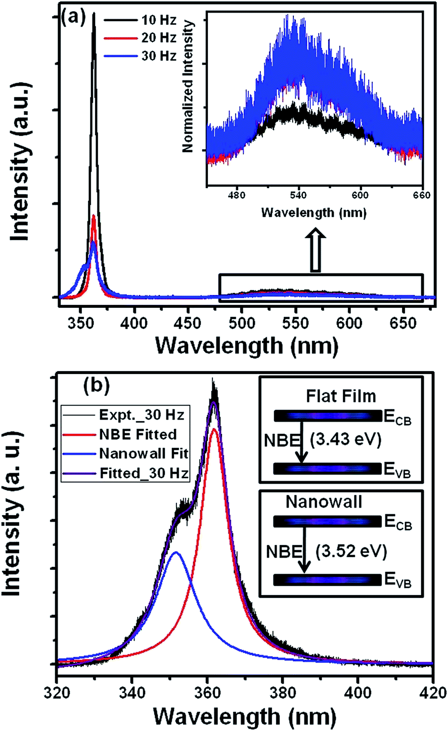 | ||
| Fig. 4 (a) Room temperature PL spectra of LMBE grown GaN nanostructures at various repetition rates. The inset shows the YL band spectra after normalization of NBE peaks. (b) PL data fitted with two Lorentzian peaks for the NBE peak of 30 Hz grown GaN nanowalls network. | ||
We have also observed an additional shoulder peak near the main NBE emission at lower wavelength side for the GaN nanowalls grown at the repetition rate of 30 Hz, as shown in Fig. 4(a). The PL emission peak of GaN films can be mostly fitted by the Lorentzian function due to the weak nature of exciton–phonon interaction.47 We have fitted the PL spectrum (near NBE region) by using two Lorentzian components correspond to NBE and shoulder peaks centered at ∼362 nm (3.43 eV) and 352 nm (3.52 eV), respectively, as shown in Fig. 4(b). Zhong et al.20 also obtained the blue shift in NBE peak (1.5 nm) for GaN nanowall grown on Si(111) compared to flat GaN film and the shift of NBE level was explained on the basis of strain related phenomena in heteroepitaxially grown GaN nanowalls network. In our case, the higher energy shoulder peak is only observed for GaN nanowalls network having low tip width (10–15 nm). In comparison with the NBE peak, the nanowall peak position blue shifts about 10 nm (90 meV). It has been estimated that one GPa biaxial strain would shift the NBE peak to ∼27 meV and Raman E2(high) mode by 4.2 cm−1.43 In our case, the shift in NBE peak is 90 meV and accordingly the E2(high) mode should have shifted by more than 12 cm−1. However, we did not see such strain related shift in E2(high) mode in Raman measurements for LMBE GaN with respect to GaN template [Fig. 3]. Recently, Bhasker et al.46 found that the NBE of GaN nanowalls (wall width ∼10 nm) was shifted by 60 meV towards higher energy side compared to that of the smooth GaN film and the enhancement of the band gap was explained on the basis of carrier confinement effect in the nanowall structures. In case of ZnO nanowalls grown on GaN template, the room temperature PL spectrum also showed the blue shift of NBE and it was attributed to the quantum confinement effect.26 In addition, the GaN nanowires of diameter comparable to Bohr exciton radius of GaN (∼11 nm) show quantum confinement effect induced blue shift was observed in PL data.48 We obtained the blue shift of NBE level only for the 30 Hz grown GaN nanowalls of with tip width of 10–15 nm, which is comparable to the Bohr exciton radius of GaN (11 nm). Therefore, we can attribute the blue shifted NBE component of nanowall network sample grown at 30 Hz to quantum confinement of the carriers.
The GaN nanowall network based devices will depend critically on the understanding of carrier relaxation in the two dimensional nanostructures. Ultrafast optical spectroscopy measurements can shed light on this aspect by measuring the carrier dynamics with femto-second time resolution. There are several ultrafast spectroscopy studies on carrier relaxation in GaN films and nanowires.49–52 However, to the best of our knowledge, there is no report on ultrafast time resolved optical measurements of GaN nanowall network. We have used ultraviolet pump pulse with wavelength of 330 nm (3.75 eV) to create electron–hole pairs across the GaN band gap (3.4 eV) as shown in Fig. 5(a) and the probe wavelength was kept at 560 nm (middle of YL band obtained from PL, 2.21 eV) to understand the carrier dynamics in our samples.
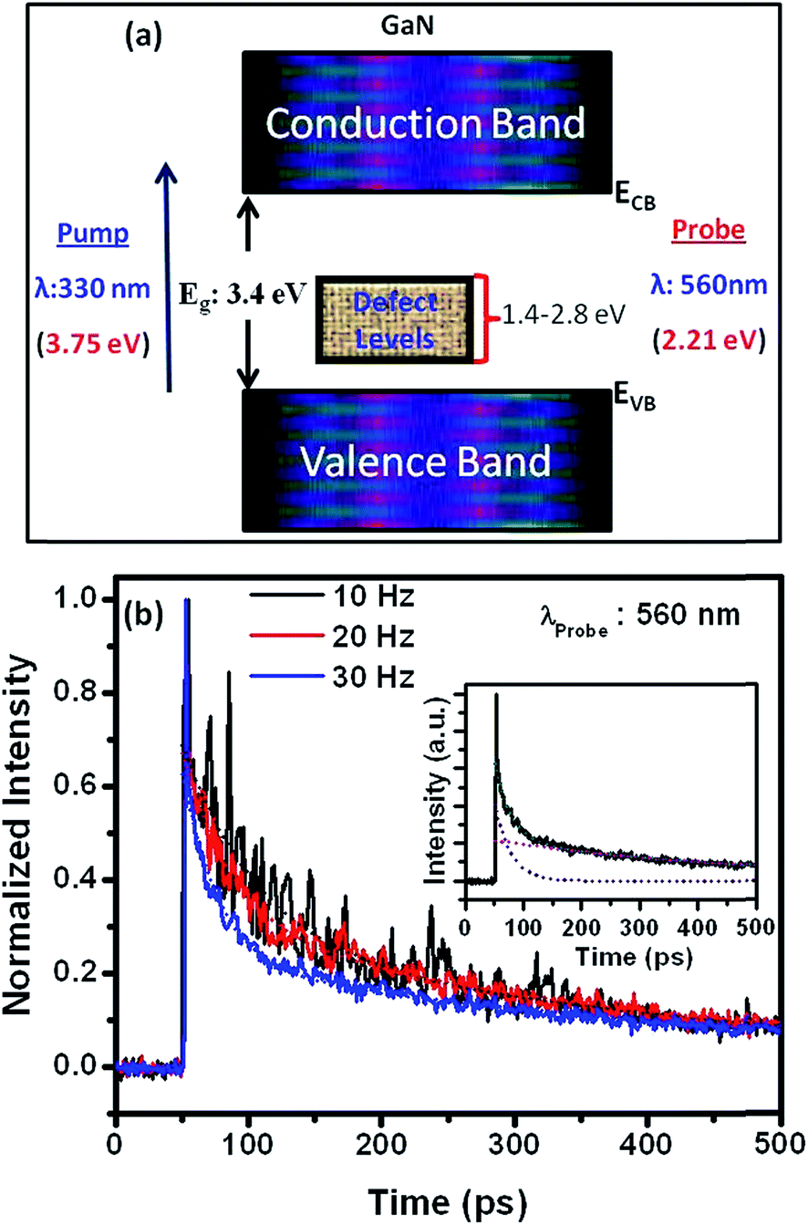 | ||
| Fig. 5 (a) Schematic of the energy band gap and defect levels in GaN, (b) ultrafast transient absorption spectra of LMBE grown GaN samples measured for pump/probe wavelength of 330 nm/560 nm. The inset of (b) shows the typical bi-exponential fitting of absorption spectrum. | ||
Fig. 5(b) shows the transient absorption spectrum with the pump/probe of 330/560 nm on LMBE grown GaN samples. The peak amplitude of all the curves was normalized to have the same height for clear comparison of carrier relaxation time. The rise time of the signal is around 50 ps irrespective of the laser repetition rates of GaN samples, which corresponds to the time for carriers to populate the deep acceptor states. In order to figure out the carrier relaxation time in GaN samples, the data were fitted with bi-exponential model functions using the relation: I = A1exp(−t/τ1) + A2exp(−t/τ2), where I is the absorption intensity, τ1 and τ2 are the fast and slow decay time constants, A1 and A2 are the amplitude.53 The τ1 and τ2 values is given in Table 1. For all the fitted data, initial fast decay constant (τ1) and slow decay constant (τ2) vary between 28–56 ps and 380–452 ps, respectively. The fast capture of electrons from the bottom of the conduction band and holes from top of the valence band is responsible for the carrier life time component τ1 in transient signal, which is free from coulomb interactions. In our case, the value of τ1 for 30 Hz grown GaN nanowall sample is smaller compared to 10 and 20 Hz grown GaN samples. The origin of the fast decay for the narrow width nanowall network is due to the carrier trapping at the edge of the nanowalls. It is not surprising as the previous reports on ultrafast pump-probe studies of Ge nanowires also showed the decrease in τ1 with decreasing nanowire diameter due to the carrier trapping at the nanowire surface.50,54 The τ2 scarcely depends on the size and the surface of the structure but is mainly due to electron–hole pair recombination. The τ2 value is larger for porous nanowalls obtained on 30 Hz grown sample. It has been reported earlier that the confined carriers recombine very slowly in semiconductor porous nanostructures.55 We recall from our PL analysis that the carrier confinement related blue shift in NBE is only observed for 30 Hz sample. It is very interesting to note that both PL and ultrafast spectroscopy measurements support quantum carrier confinement in the GaN nanowall of tip width 10–15 nm.
3.3. Electronic structures of GaN film and nanowalls network
Even though there are several studies available now about the growth of GaN nanowall network15,18–22,56 and their structural and optical properties,18–22 electronic structure of GaN nanowall network has been scarcely explored. Recently, using XPS, Thakur et al. compared the electronic structure of GaN nanowall network grown on c-plane sapphire substrate to a MOCVD grown GaN template (epilayer).57 They have fitted the valence band (VB) spectra using multiple peaks and claimed that this fitting was based on the same procedure as of CL spectrum. In their case, XPS data was acquired using non-monochromatic Mg Kα X-ray source and therefore VB energy region could be affected due to the presence of Ga 3d related Kα3,4 X-ray satellites. In our case, for non-monochromatic Mg Kα X-ray source, great care has been taken for additional satellites peak.Here, we have utilized the monochromatic Al Kα source to perform XPS studies as it is free from additional X-ray satellites and provides much better energy resolution compared to non-monochromatic X-ray source. Fig. 6 shows the Ga 3d and N 1s core level spectra of MOCVD grown GaN template (bottom) and LMBE grown (10 Hz: middle and 30 Hz: top) GaN samples. We have performed χ2 iterative fit of Ga 3d and N 1s core level spectra to determine accurate peak positions and relative contribution of different species. Ga 3d core level spectra of GaN template and LMBE grown sample at 10 Hz repetition rate can be fitted using 2 components (Ga–N and Ga–O) while a third component (Ga–Ga) is also required for the fitting of Ga 3d core level spectrum of LMBE grown GaN nanowall network (30 Hz) as shown in Fig. 6(a). N 2s related component is also shown. Fitting parameters are summarized in Table 2. All the Ga 3d core level spectra are dominated by Ga–N main peak which appears at 19.95 ± 0.05 eV for GaN template and LMBE grown 10 Hz sample while it appears at 20.1 ± 0.05 eV for GaN nanowall network (30 Hz). Peak position and FWHM values for GaN template are close to the earlier reports.58,59 Peak FWHM increases for LMBE grown samples and it is highest for sample grown at 30 Hz repetition rate. Ga–O component is observed at 1.2 eV higher BE side compared to main peak and it can be attributed to the formation of Ga2O3 at the surface due to atmospheric exposure to samples.60,61 Ga–Ga component is located at 1.0 eV lower BE side compared to main peak and it can be related to uncoordinated/metallic Ga atoms.59,60 Relative percentage of Ga–O varies very little (7.2 to 7.9) between different samples and it indicates similar amount of surface oxidation for all the samples.
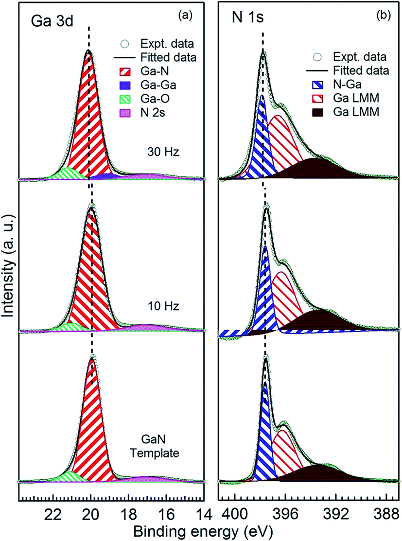 | ||
| Fig. 6 (a) Ga 3d core level spectra of GaN template and LMBE grown GaN (10 and 30 Hz) on template. Experimental data (open circles), fitted spectra (thick solid line), deconvoluted components used to fit Ga–N (thick red patterned), Ga–Ga (violet shaded), Ga–O (thin green patterned) and N 2s (pink shaded) are also shown. (b) N 1s core level spectra along with Ga Auger features of GaN template and laser MBE grown (10 and 30 Hz) GaN on template. Experimental data (open circles), fitted spectra (thick solid line), deconvoluted components used to fit N–Ga (thick blue patterned) and Ga LMM Auger features (thin green patterned and dark brown shaded) are also shown. Each set of spectra have been normalized by the peak height of the highest peak and staggered along the y axis for clarity of presentation. Dashed lines indicate the peak positions. | ||
| Sample | GaN template | 10 Hz LMBE GaN | 30 Hz LMBE GaN | ||||||
|---|---|---|---|---|---|---|---|---|---|
| Peak | FWHM | Relative% | Peak | FWHM | Relative% | Peak | FWHM | Relative% | |
| Ga 3d (Al Kα) | Ga–N | 1.1 | 92.5 | Ga–N | 1.19 | 92.8 | Ga–N | 1.23 | 87.2 |
| Ga–O | 1.12 | 7.5 | Ga–O | 1.2 | 7.2 | Ga–O | 1.1 | 7.9 | |
| Ga–Ga | 1.51 | 4.9 | |||||||
| N 1s (Al Kα) | N–Ga | 0.85 | 30.5 | N–Ga | 1.03 | 26.7 | N–Ga | 1.1 | 26.8 |
| Ga LMM | 2.42 | 44.5 | Ga LMM | 2.68 | 46.4 | Ga LMM | 3.0 | 50.5 | |
| Ga LMM | 4.32 | 25.0 | Ga LMM | 4.3 | 26.9 | Ga LMM | 4.24 | 22.7 | |
| N 1s (Mg Kα) | N–Ga | 1.17 | 86.6 | N–Ga | 1.4 | 90.6 | N–Ga | 1.45 | 89.4 |
| NH + NH2 | 1.49 | 10.2 | NH + NH2 | 1.49 | 9.4 | NH + NH2 | 1.49 | 10.6 | |
| N–H3 | 1.49 | 3.2 | |||||||
| Valence band (Al Kα) | A | 2.1 | 42.6 | A | 2.41 | 46.2 | A | 2.44 | 48.3 |
| B | 2.56 | 32.3 | B | 2.37 | 27.6 | B | 2.42 | 29.4 | |
| C | 1.3 | 25.1 | C | 1.56 | 26.2 | C | 1.56 | 22.3 | |
N 1s core level spectra have been fitted using 3 components (N–Ga and 2 components for Ga LMM Auger features) as shown in Fig. 6(b).58 N–Ga peak appears at 397.6 ± 0.05 eV for GaN template and LMBE grown 10 Hz sample while it appears at 397.8 ± 0.05 eV for GaN nanowall network grown at 30 Hz repetition rate. Ga related Auger features appear at 1.3 and 4.1 eV lower BE side compared to main peak (N–Ga). Energy position and FWHM values for GaN template are close to earlier reported values.58,59,62 Fitting parameters are summarized in Table 2. Similar to Ga 3d spectra, FWHM of N–Ga increases for LMBE grown samples and it is highest for nanowall network grown at 30 Hz. XPS core level spectroscopy is one the most powerful technique to determine the surface chemical composition. Even though use of monochromatic Al Kα source has advantage of better resolution, it makes the N 1s core level spectra more complicated as it overlaps with broad Ga Auger features (Fig. 6(b)). Therefore, N 1s core levels recorded with monochromatic Al Kα source are not ideal to determine the chemical composition of GaN. However, use of non-monochromatic Mg Kα solves this problem as Ga Auger features do not overlap with N 1s core level any more.63 Fig. 7 shows N 1s core level spectra acquired using non-monochromatic Mg Kα source. For LMBE grown samples, spectra can be fitted by 2 peaks (N–Ga and N–H/N–H2). N–Ga peak dominates the spectra and surface contamination related N–H/N–H2 component appears at 1.5 eV higher BE side.59,62 However, for GaN template, we also observed a small feature at 3.0 eV higher BE side which can be attributed to NH3 contamination occurred during MOCVD growth.62 Fitting parameters are summarized in Table 2. N–Ga peak positions are similar to data acquired using monochromatic Al Kα (Fig. 6(b)). We have also recorded Ga 3d core level spectra using non-monochromatic Mg Kα source (not shown here) to determine Ga to N ration of GaN template and LMBE grown samples. These Ga 3d core level spectra have been fitted using exactly same procedure as adopted to fit Ga 3d core level spectra measured using monochromatic Al Kα source. Only change was observed in FWHM values as it increases due to increased line width of non-monochromatic X-ray source.
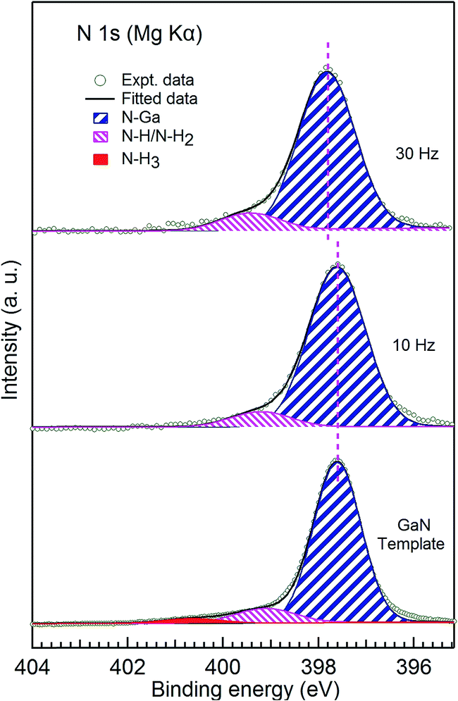 | ||
| Fig. 7 N 1s core level spectra of GaN template and LMBE grown GaN (10 and 30 Hz) on template. Experimental data (open circles), fitted spectra (thick solid line), deconvoluted components used to fit N–Ga (thick blue patterned), N–H + N–H2 (thin pink patterned) and N–H3 (red shaded) are also shown. Each set of spectra have been normalized by the peak height of the highest peak and staggered along the y axis for clarity of presentation. Dashed lines indicate the peak positions. All the spectra have been acquired using non-monochromatic Mg Kα X-ray source. | ||
Area under the curve of Ga 3d and N 1s core levels have been normalized using respective photo ionization cross sections, inelastic mean free path and analyzer transmission function.63–65 Normalized area ratio have been used to calculate the surface chemical composition of the GaN samples. Calculated Ga/N ratio turned out to be 1.04 ± 0.05, 1.19 ± 0.06 and 2.03 ± 0.1 for GaN template, LMBE grown samples at 10 Hz and 30 Hz, respectively. It clearly indicates that the LMBE grown samples contain more Ga and the Ga/N ratio is highest for GaN nanowall network grown at 30 Hz. It has been reported that Ga rich surface may result due to formation of Ga adlayer and/or Ga droplets and it can result in surface reconstructions.66–68 Surface sensitivity of XPS can be tuned by varying the photoemission angle. As we decrease the photoemission angle and go towards grazing emission angle, more and more signal will be coming from near surface region while signal from deeper layers will be mainly collected at normal emission angle. Therefore, we should observe clear increase in the Ga/N ratio at near grazing emission photoemission angles in case of presence of Ga adlayer at the surface. We have plotted Ga/N ration of LMBE grown GaN nanowall network (30 Hz) at various photoemission angles in Fig. 8. We do not observe clear increase in Ga/N ratio at near grazing emission photoemission angle within our experimental error. Therefore, we can exclude the possibility of excess Ga at surface and Fig. 8 suggests that Ga/N ratio remains almost similar within the probing depth of XPS. Higher Ga/N ratio for LMBE grown GaN nanowall network (30 Hz) suggests that it will have largest number of N vacancy related defects and it can be correlated with the defect density observed in this sample (Fig. 1(d)). Largest number of N vacancies in LMBE grown GaN nanowall network (30 Hz) can also explain the enhanced peak intensity of YL band on PL spectrum (inset of Fig. 4(a)).69 Ga 3d and N 1s core levels of LMBE grown nanowall network (30 Hz) shifts towards higher BE side by 0.15 and 0.2 eV, respectively compared to GaN template and such shifts have been attributed to the presence of N vacancies in GaN.70–73 In recent past, N vacancies have emerged as major point defect in bulk and nanostructured GaN.74–76 Fitting of Ga 3d core level spectrum (Fig. 6(a)) of LMBE grown nanowall network (30 Hz) confirmed the formation of uncoordinated/metallic Ga atoms in the sample, which also points towards the presence of N vacancies. Gao et al. reported that Ga–Ga split interstitials play very important role in the formation of GaN nanowires.76 For LMBE grown nanowall network (30 Hz), uncoordinated Ga atoms may be located at interstitial sites and these could play an important role in engineering a GaN nanowall network. However, further model calculations will be required to test this hypothesis.
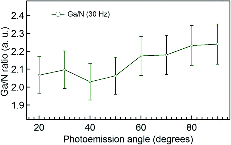 | ||
| Fig. 8 Ga/N ratio plotted as a function of photoemission angle for LMBE grown GaN (30 Hz) on template. Ga 3d and N 1s core levels acquired using non-monochromatic Mg Kα X-ray source have been used to determine the ratio. Error bars representing experimental uncertainty (±5% of the base value) in quantification are also shown. | ||
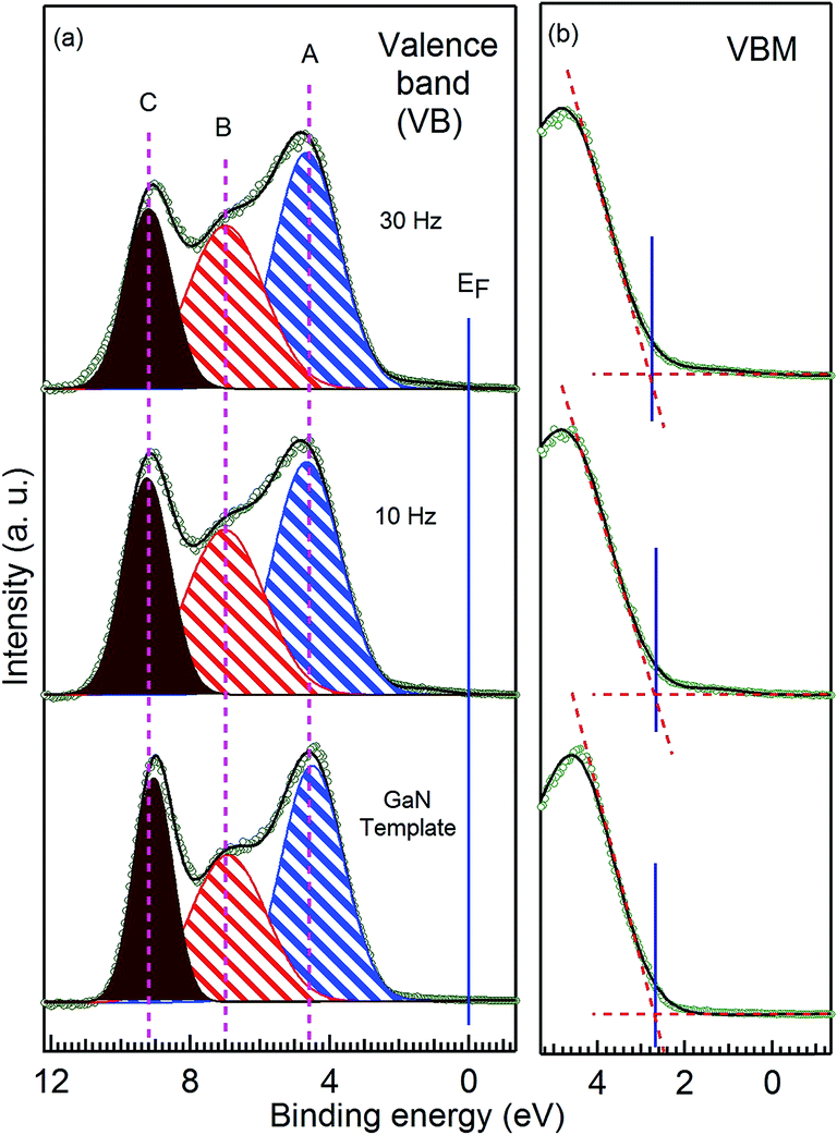
We compare the VB spectra of GaN template and LMBE grown GaN samples in Fig. 9(a) and dashed lines clearly show that VB is dominated by 3 components (A, B and C). Peak A, and C are related to Ga 4p–N 2p and Ga 4s–N 2p hybridized states, respectively with N 2p dominant character whereas peak B has been attributed to mixed orbitals and/or surface adsorbates.77 Line shape of the XPS VB spectra and energy position of dominant features are in good agreement with earlier reports.77–79 VB spectra can be satisfactorily fitted using 3 components corresponding to features A, B and C. Fitting parameters are summarized in Table 2. For GaN template, feature A, B and C appeared at 4.5 ± 0.5, 6.92 ± 0.5, and 9.1 ± 0.5, respectively. Similar to core levels, FWHM of VB peaks also increases for LMBE grown samples compared to GaN template which could be correlated to increased defect density. BE position of all the features of VB remains same for LMBE grown GaN. There is very small shift towards higher BE for peak A and C for LMBE grown samples compared to GaN template. It is evident from Fig. 9(a) and Table 2 that redistribution of spectral weight takes place in LMBE grown samples compared to GaN template and it can be attributed to change in Ga/N ratio and consequent change in Ga–N hybridization.
 | ||
| Fig. 9 (a) Valence band spectra of GaN template and LMBE grown GaN (10 and 30 Hz) on template. Experimental data (open circles), fitted spectra (thick solid line), deconvoluted components used to fit peak “A” (blue patterned), peak “B” (red patterned) and peak “C” (dark brown shaded) are also shown. Each set of spectra have been normalized by the peak height of the highest peak and staggered along the y axis for clarity of presentation. Dashed lines indicate the peak positions. Solid line indicates the position of Fermi level (EF). (b) Near EF region and valence band maxima position (indicated by solid lines) along with two linear fits of leading edge and base line (shown by dashed lines). | ||
Fig. 9(b) shows the near EF region for all the GaN samples. The position of valence band maxima (VBM) has been determined from the extrapolation of two linear fits (dashed lines) of leading edge and base line.63 It turns out that VBM lies at 2.67 ± 0.05, 2.68 ± 0.05, and 2.78 ± 0.05 eV below surface Fermi level for GaN template and LMBE grown samples at 10 and 30 Hz, respectively. Considering energy band gap (Eg) of GaN to ∼3.4 eV, VBM positions confirm that GaN template and the unintentional doped LMBE grown GaN samples shows n-type conductivity. Similar to BE shift in core levels, VBM of LMBE grown GaN nanowall network (30 Hz) is shifted by ∼0.1 eV towards higher BE compared to MOCVD grown flat GaN template. We recall that our PL spectrum for LMBE grown GaN nanowall network (30 Hz) shows the increase in band gap by 0.09 eV and VBM shift towards higher BE side may be correlated to increase in band gap. Alternatively, higher BE shift of VBM and Ga 3d and N 1s core levels may also result due to the N vacancy induced change in surface band bending. N vacancies related donor states may increase near surface electron concentration resulting in positive surface charge. It will result in reduction of positive space charge in depletion region and lower band bending. Position of VBM and core level BE can also be affected due to varying order of surface oxidation of GaN surface.80 However, in our case, surface oxidation will not affect the data analysis as we have similar order of surface contamination on all our analyzed sample (Table 2). We have not observed any defect induced states in the energy gap (between VBM and EF). Even if such states exist, we may not be able to observe as these states could be hybridized with edge states and buried below the VBM.75 We also do not find any evidence of presence of metallic states related to uncoordinated Ga atoms as we do not see any spectral weight around EF.
4. Conclusion
The GaN nanowall networks were grown on GaN templates using LMBE system by ablation of HVPE grown solid GaN target in presence of r.f. nitrogen plasma at substrate temperature 700 °C. The effect of the laser repetition rate (10, 20 and 30 Hz) on the structural, optical and electronic properties of the GaN nanostructures. FESEM study showed that the GaN nanowall width decreases as a function of laser repetition rate and a nanowall tip width of 10–15 nm and pore size of 120–180 nm is obtained for 30 Hz grown sample. The PL measurement shows a blue shift of the band edge luminescence for 30 Hz sample due to the one dimensional confinement of carriers at the top edges of the nanowalls as complimented by the ultrafast spectroscopy measurements. We have studied the electronic structure of GaN nanowall network using high resolution XPS and compared it with 2-dimensional, flat GaN template. Ga/N ratio calculated from Ga 3d and N 1s is found to be highest (∼2) for nanowall network grown at highest laser repetition rate and its core level spectra shift towards higher BE side compared to GaN template. High Ga/N ratio, core level BE shift and change in VBM position with respect to EF provide strong evidence of larger number of N vacancy related defect states in nanowall network grown at 30 Hz laser repetition rate. XPS VB spectra also demonstrate the decreased surface band bending of GaN nanowall network grown at 30 Hz. The grown GaN nanowall network having reduced volume in comparison to dense films can have potential technological application as nitride based high temperature sensors81 and high brightness optoelectronic devices.Acknowledgements
The authors are grateful to Director, NPL for his constant encouragement and support. SSK and MSK are thankful to Dr T. D. Senguttuvan and Ms M. Kaur for their kind supports in FESEM measurement. This work has been financially supported by Council of Scientific and Industrial Research (CSIR) under networking project PSC0109.References
- S. Nakamura, Science, 1998, 281, 956 CrossRef CAS.
- F. A. Ponce and D. P. Bour, Nature, 1997, 386, 351 CrossRef CAS PubMed.
- S. Nakamura and S. F. Chichibu, Introduction to Nitride Semiconductor Blue Lasers and Light Emitting Diodes, CRC Press, United States, 2000 Search PubMed.
- R. Dahal, B. Pantha, J. Li, J. Y. Lin and H. X. Jiang, Appl. Phys. Lett., 2009, 94, 063505 CrossRef PubMed.
- J. Ma, X. Zhu, K. M. Wong, X. Zou and K. M. Lau, J. Cryst. Growth, 2013, 370, 265 CrossRef CAS PubMed.
- C. F. Huang, W. Y. Hsieh, B. C. Hsieh, C. H. Hsieh and C. F. Lin, Thin Solid Films, 2013, 529, 278 CrossRef CAS PubMed.
- H. Sun, J. Woodward, J. Yin, A. Moldawer, E. F. Pecora, A. Yu. Nikiforov, L. D. Negro, R. Paiella, K. Ludwig Jr, D. J. Smith and T. D. Moustakas, J. Vac. Sci. Technol., B: Nanotechnol. Microelectron.: Mater., Process., Meas., Phenom., 2013, 31, 03C117 Search PubMed.
- L. Shang, T. Lu, G. Zhai, Z. Jia, H. Zhang, S. Ma, T. Li, J. Liang, X. Liu and B. Xu, RSC Adv., 2015, 5, 51201 RSC.
- W. Yang, W. Wang, Z. Liu, Y. Lin, S. Zhou, H. Qian and G. Li, CrystEngComm, 2015, 17, 1073 RSC.
- S. D. Hersee, Y. Sun and X. Wang, Nano Lett., 2006, 6, 1808 CrossRef CAS PubMed.
- W. C. Hou, T. H. Wu, W. C. Tang and F. C. N. Hong, Nanoscale Res. Lett., 2012, 7, 373 CrossRef PubMed.
- J. Goldberger, R. He, Y. Zhang, S. Lee, H. Yan, H. J. Choi and P. Yang, Nature, 2003, 422, 599 CrossRef CAS PubMed.
- S. W. Kim, Y. H. Park, I. Kim, T. E. Park, B. W. Kwon, W. K. Choi and H. J. Choi, Nanoscale, 2013, 5, 8550 RSC.
- V. Purushothaman, P. S. Venkatesh, R. Navamathavan and K. Jeganathan, RSC Adv., 2014, 4, 45100 RSC.
- D. Poppitz, A. Lotnyk, J. W. Gerlach and B. Rauschenbach, Acta Mater., 2014, 65, 98 CrossRef CAS PubMed.
- S. Jiang, J. Zhang, X. Qi, M. He and J. Li, CrystEngComm, 2013, 15, 9837 RSC.
- J. Li, J. Liu, L.-S. Wang and R. P. H. Chang, Inorg. Chem., 2008, 47, 10325 CrossRef CAS PubMed.
- M. Kesaria, S. Shetty and S. M. Shivaprasad, Cryst. Growth Des., 2011, 11, 4900 CAS.
- A. Zhong and K. Hane, Nanoscale Res. Lett., 2012, 7, 686 CrossRef PubMed.
- A. Zhong and K. Hane, Jpn. J. Appl. Phys., 2013, 52, 08JE13 CrossRef.
- V. Thakur, M. Kesaria and S. M. Shivaprasad, Solid State Commun., 2013, 171, 8 CrossRef CAS PubMed.
- M. Kesaria and S. M. Shivaprasad, Appl. Phys. Lett., 2011, 99, 143105 CrossRef PubMed.
- C. C. Wu, D. S. Wuu, T. N. Chen, T. E. Yu, P. R. Lin, R. H. Horng and S. Sun, J. Nanosci. Nanotechnol., 2008, 8, 3851 CrossRef CAS PubMed.
- S. W. Kim, H. K. Park, M. S. Yi, N. M. Park, J. H. Park, S. H. Kim, S. L. Maeng, C. J. Choi and S. E. Moon, Appl. Phys. Lett., 2007, 90, 033107 CrossRef PubMed.
- Z. Shi, Y. Zhang, J. Zhang, H. Wang, B. Wu, X. Cai, X. Cui, X. Dong, H. Liang, B. Zhang and G. Du, Appl. Phys. Lett., 2013, 103, 021109 CrossRef PubMed.
- C. C. Wu, D. S. Wuu, T. N. Chen, T. E. Yu, P. R. Lin, R. H. Horng and H. Y. Lai, Jpn. J. Appl. Phys., 2008, 47, 746 CrossRef CAS.
- M. S. Kumar, S. S. Kushvaha and K. K. Maurya, Sci. Adv. Mater., 2014, 6, 1215 CrossRef CAS PubMed.
- S. S. Kushvaha, M. S. Kumar, K. K. Maurya, M. K. Dalai and N. D. Sharma, AIP Adv., 2013, 3, 092109 CrossRef PubMed.
- G. Li, S. J. Shih and Z. Fu, Chem. Commun., 2010, 46, 1206 RSC.
- W. Wang, Y. Lin, W. Yang, Z. Liu, S. Zhiou, H. Qian, F. Gao, L. Wen and G. Li, J. Mater. Chem. C, 2014, 2, 4112 RSC.
- D. A. Shirley, Phys. Rev. B: Solid State, 1972, 5, 4709 CrossRef.
- E. J. Tarsa, B. Heying, X. H. Wu, P. Fini, S. P. DenBaara and J. S. Speck, J. Appl. Phys., 1997, 82, 5472 CrossRef CAS PubMed.
- P. Gay, P. B. Hirsch and A. Kelly, Acta Metall., 1953, 1, 315 CrossRef CAS.
- M. A. Moram and M. E. Vickers, Rep. Prog. Phys., 2009, 72, 036502 CrossRef.
- B. Heying, R. Averbeck, L. F. Chen, E. Haus, H. Riechert and J. S. Speck, J. Appl. Phys., 2000, 88, 1855 CrossRef CAS PubMed.
- K. A. Bertness, A. Roshko, L. M. Mansfield, T. E. Harvey and N. A. Sanford, J. Cryst. Growth, 2008, 310, 3154 CrossRef CAS PubMed.
- T. B. Wei, R. F. Duan, J. X. Wang, J. M. Li, Z. Q. Huo and Y. P. Zheng, Microelectron. J., 2008, 39, 1556 CrossRef CAS PubMed.
- Z. C. Feng, W. Wang, S. J. Chua, P. X. Zhang, K. P. J. Williams and G. D. Pitt, J. Raman Spectrosc., 2001, 32, 840 CrossRef CAS PubMed.
- A. Kasic, D. Gogova, H. Larsson, C. Hemmingsson, I. Ivanov, B. Monemar, C. Bundesmann and M. Schubert, Phys. Status Solidi A, 2004, 201, 2773 CrossRef CAS PubMed.
- X. Hai-Ying, N. Ping-Juan and X. Yu-Xin, Chin. Phys. B, 2012, 21, 077801 CrossRef.
- X. Liu, D. Li, X. Sun, Z. Li, H. Song, H. Jiang and Y. Chen, CrystEngComm, 2014, 16, 9058 Search PubMed.
- V. Yu. Davydov, Yu. E. Kitaev, I. N. Goncharuk, A. N. Smirnov, J. Graul, O. Semchinova, D. Uffman, M. B. Smirnov, A. P. Mirgorodsky and R. A. Evarestov, Phys. Rev. B: Condens. Matter Mater. Phys., 1998, 58, 12899 CrossRef CAS.
- C. Kisielowski, J. Kruger, S. Ruvimov, T. Suski, J. W. Ager III, E. Jones, Z. Liliental-Weber, M. Rubin, E. R. Weber, M. D. Bremser and R. F. Davis, Phys. Rev. B: Condens. Matter Mater. Phys., 1996, 54, 17745 CrossRef CAS.
- M. A. Reshchikov and H. Morkoc, J. Appl. Phys., 2005, 97, 061301 CrossRef PubMed.
- M. Kesaria, S. Shetty and S. M. Shivaprasad, J. Cryst. Growth, 2011, 326, 191 CrossRef CAS PubMed.
- H. P. Bhasker, S. Dhar, A. Sain, M. Kesaria and S. M. Shivaprasad, Appl. Phys. Lett., 2012, 101, 132109 CrossRef PubMed.
- G. D. Chen, M. Smith, J. Y. Lin, H. X. Jiang, M. A. Khan and C. J. Sun, Appl. Phys. Lett., 1995, 67, 1653 CrossRef CAS PubMed.
- B. Ha, S. H. Seo, J. H. Cho, C. S. Yoon, J. Yoo, G. C. Yi, C. Y. Park and C. J. Lee, J. Phys. Chem. B, 2005, 109, 11095 CrossRef CAS PubMed.
- C. K. Choi, Y. H. Kwon, J. S. Krasinski, G. H. Park, G. Setlur, J. J. Song and Y. C. Chang, Phys. Rev. B: Condens. Matter Mater. Phys., 2001, 63, 115315 CrossRef.
- R. P. Prasankumar, P. C. Upadhya and A. J. Taylor, Phys. Status Solidi B, 2009, 246, 1973 CrossRef CAS PubMed.
- C. K. Sun, Y. L. Huang, S. Keller, U. K. Mishra and S. P. DenBaars, Phys. Rev. B: Condens. Matter Mater. Phys., 1999, 59, 13535 CrossRef CAS.
- P. C. Upadhya, Q. Li, G. T. Wang, A. J. Fischer, A. J. Taylor and R. P. Prasankumar, Semicond. Sci. Technol., 2010, 25, 024017 CrossRef.
- R. Klann, O. Brandt, H. Yang, H. T. Grahn and K. H. Ploog, Appl. Phys. Lett., 1997, 70, 1808 CrossRef CAS PubMed.
- R. P. Prasankumar, S. Choi, S. A. Trugman, S. T. Picraux and A. J. Taylor, Nano Lett., 2008, 8, 1619 CrossRef PubMed.
- Y. Kanemitsu, Phys. Rev. B: Condens. Matter Mater. Phys., 1993, 48, 12357 CrossRef CAS.
- U. K. Gautam, S. R. C. Vivekchand, A. Govindaraj and C. N. R. Rao, Chem. Commun., 2005, 3995 RSC.
- V. Thakur and S. M. Shivaprasad, Appl. Surf. Sci., 2015, 327, 389 CrossRef CAS PubMed.
- M. R. Coan, J. H. Woo, D. Johnson, I. R. Gatabi and H. R. Harris, J. Appl. Phys., 2012, 112, 024508 CrossRef PubMed.
- D. Li, M. Sumiya, S. Fuke, D. Yang, D. Que, Y. Suzuki and Y. Fukuda, J. Appl. Phys., 2001, 90, 4219 CrossRef CAS PubMed.
- S. D. Wolter, B. P. Luther, D. L. Waltemyer, C. Önneby, S. E. Mohney and R. J. Molnar, Appl. Phys. Lett., 1997, 70, 2156 CrossRef CAS PubMed.
- M. Petravic, V. A. Coleman, K. J. Kim, B. Kim and G. Li, J. Vac. Sci. Technol., A, 2005, 23, 1340 CAS.
- Y.-J. Lin, C.-D. Tsai, Y.-T. Lyu and C.-T. Lee, Appl. Phys. Lett., 2000, 77, 687 CrossRef CAS PubMed.
- S. S. Kushvaha, M. Senthil Kumar, M. Maheshwari, A. K. Shukla, P. Pal and K. K. Maurya, Mater. Res. Express, 2014, 1, 035903 CrossRef PubMed.
- J. J. Yeh and I. Lindau, At. Data Nucl. Data Tables, 1985, 32, 1 CrossRef CAS.
- S. Tanuma, C. J. Powell and D. R. Penn, Surf. Interface Anal., 1993, 21, 165 CrossRef PubMed.
- G. Koblmüller, J. Brown, R. Averbeck, H. Riechert, P. Pongratz and J. S. Speck, Appl. Phys. Lett., 2005, 86, 041908 CrossRef PubMed.
- S. H. Xu, H. Wu, X. Q. Dai, W. P. Lau, L. X. Zheng, M. H. Xie and S. Y. Tong, Phys. Rev. B: Condens. Matter Mater. Phys., 2003, 67, 125409 CrossRef.
- A. R. Smith, R. M. Feenstra, D. W. Greve, J. Neugebauer and J. E. Northrup, Phys. Rev. Lett., 1997, 79, 3934 CrossRef CAS.
- W. Lei, D. Liu, J. Zhang, B. Liu, P. Zhu, T. Cui, Q. Cui and G. Zou, Chem. Commun., 2009, 1365 RSC.
- K. A. Rickert, A. B. Ellis, F. J. Himpsel, J. Sun and T. F. Kuech, Appl. Phys. Lett., 2002, 80, 204 CrossRef CAS PubMed.
- H. W. Jang and J. L. Lee, Appl. Phys. Lett., 2009, 94, 182108 CrossRef PubMed.
- T. Hashizume and R. Nakasaki, Appl. Phys. Lett., 2002, 80, 4564 CrossRef CAS PubMed.
- J. Lin and Y. L. Chu, J. Appl. Phys., 2005, 97, 104904 CrossRef PubMed.
- M. G. Ganchenkova and R. M. Nieminen, Phys. Rev. Lett., 2006, 96, 196402 CrossRef CAS.
- D. J. Carter, M. Fuchs and C. Stampfl, J. Phys.: Condens. Matter, 2012, 24, 255801 CrossRef PubMed.
- F. Gao, E. J. Bylaska, A. El-Azab and W. J. Webber, Appl. Phys. Lett., 2004, 85, 5565 CrossRef CAS PubMed.
- W. R. L. Lambrecht, B. Segall, S. Strite, G. Martin, A. Agarwal, H. Morkoc and A. Rockett, Phys. Rev. B: Condens. Matter Mater. Phys., 1994, 50, 14155 CrossRef CAS.
- P. Lorenz, T. Haensel, R. Gutt, R. J. Koch, J. A. Schaefer and S. Krischok, Phys. Status Solidi B, 2010, 247, 1658 CrossRef CAS PubMed.
- D. Skuridina, D. V. Dinh, B. Lacroix, P. Ruterana, M. Hoffmann, Z. Sitar, M. Pristovsek, M. Kneissl and P. Vogt, J. Appl. Phys., 2013, 114, 173503 CrossRef PubMed.
- M. A. Garcia, S. D. Wolter, T.-H. Kim, S. Choi, J. Baier, A. Brown, M. Losurdo and G. Bruno, Appl. Phys. Lett., 2006, 88, 013506 CrossRef PubMed.
- S. Siddhanta, V. Thakur, C. Narayana and S. M. Shivaprasad, ACS Appl. Mater. Interfaces, 2012, 4, 5807 CAS.
| This journal is © The Royal Society of Chemistry 2015 |