
Fabricating a morphology tunable patterned bio-inspired polydopamine film directly via microcontact printing†
Yanshan Hou‡
ab,
Peng Xiao‡b,
Jiawei Zhang*b,
Meiwen Pengb,
Wei Lub,
Youju Huangb,
Chunfa Ouyang*a and
Tao Chen*b
aSchool of Materials Science & Engineering, Shanghai Institute of Technology, Shanghai 201418, China. E-mail: ouyoung_0916@163.com
bDivision of Polymer and Composite Materials, Ningbo Institute of Material Technology and Engineering, Chinese Academy of Science, 1219 Zhongguan West Road, Ningbo 315201, China. E-mail: zhangjiawei@nimte.ac.cn; tao.chen@nimte.ac.cn
First published on 9th July 2015
Abstract
A robust and simple strategy of microcontact printing is provided to fabricate micro-patterned polydopamine (PDA) films with tunable morphology achieved by altering the concentration of PDA “ink” solution. Photoactive sites on the surface of patterned PDA films allow the further growth of polymer brushes by self-initiated photografting and photopolymerization (SIPGP) endowing the bio-inspired PDA films with various functionalities.
Inspired by the adhesive proteins produced by mussels, polydopamine (PDA), which can be easily polymerized from dopamine in the presence of oxygen in slightly basic aqueous conditions, has the ability to adhere to various substrates with controllable thickness and durable stability.1,2 Moreover, it has been proved that PDA has good biocompatibility and low toxicity, therefore PDA has attracted tremendous interest and shown promising applications in surface modification in biological and biomedical fields.3,4
Patterned surfaces play a considerable role in modification of surface properties and have attracted extensive interest because of their potential applications in many surface-based technologies such as protein-resistant coatings, sensors, and substrates for cell-growth control.5–9 In general, micropatterns can be fabricated by a variety of techniques including photo lithography,10 electron-beam lithography,11 electron-beam chemical lithography,12 soft lithography,13,14 etc. Among these lithographic approaches, microcontact printing (μCP)15,16 is one of the most popular fabrication techniques for creating nano- and micro-structures because of its convenience, facility, rapidness and low-cost. Recently, PDA patterns were transferred from a PDMS stamp to various substrates via μCP, which provides a powerful tool for the development of tunable patterned substrates for cell and protein patterning.8 Zhou et al. reported stratified polymer brushes were fabricated using μCP of initiator integrated PDA on polymer brush surfaces and the following surface initiated atom transfer radical polymerization (SI-ATRP).15 However, these PDA are mostly modified or deposited on the PDMS for a long time.
In our previous work, we have presented robust and scalable approaches for fabricating patterned polymer brushes on various OH-terminated substrates via μCP induced supramolecular self-assembly of small molecules or GO nanosheets and subsequent self-initiated photografting and photopolymerization (SIPGP).17–19 However, various patterns cannot be easily produced from one single stamp during the process of μCP. There is considerable demand to create complex polymer microstructures because the properties of materials are highly dependent on the complexity of the structures. In order to increase the adhesion properties of ink molecules and obtain patterned films with controllable structures, in the present work, biocompatible molecules PDA were directly applied as “ink” molecules to fabricate patterned surface via μCP, and the structure and the thickness of PDA micropatterns can be easily tuned by adjusting the concentration of PDA “ink” solution. Moreover, the photoactive sites on PDA surface can be initiated to grow polymer brushes without a surface bonded initiator, and endowing the functionality of self-assembly patterns. Our approach provides a simple method to generate patterned polymer films with various tunable structures.
The procedure for fabricating patterned PDA architectures via μCP directed supramolecular self-assembly is schematically shown in Fig. 1. PDA solution can be easily prepared by dopamine solutions in the presence of tris(hydroxymethyl)aminomethane (Fig. S1†).20 A PDA solution inked polydimethylsiloxane (PDMS) stamp was primarily made to contact with the OH-terminated silicon substrate by gentle force (Fig. 1A and B). The OH groups on the silicon surface will interact with the HO- or NH2-terminated PDA derivatives through multiple hydrogen bonds. Therefore, micro-patterned PDA is easily transferred from the PDMS stamp onto the silicon wafer when the stamp is removed after μCP. Moreover, when the concentration of the PDA “ink” solution is increased, the morphology of the PDA pattern can be regulated (Fig. 1C–E).
 | ||
| Fig. 1 Schematic representation of fabricating tunable micro-patterned PDA films via μCP directed supramolecular self-assembled PDA on the silicon substrate. | ||
Atomic force microscopy (AFM) is applied to observe the morphology of patterned PDA microstructures. Fig. 2 shows AFM height images of various patterned PDA microstructures created by changing the concentration of PDA solution. When the PDA solution is relatively dilute (1 mg mL−1, 2 mg mL−1, 4 mg mL−1), the shape of the formed PDA pattern on the silicon substrate is transferred from the surface of PDMS stamp (Fig. 2A–C). The height of obtained images increases with increasing concentration of PDA solution (Fig. 2I). When the concentration of PDA solution increases to 5 mg mL−1, grid and ring patterns exist simultaneously (Fig. 2D). As shown in Fig. 2J, the height of the grid pattern is ∼40 nm, which is similar to Fig. 2C, and the height of the ring pattern is ∼30 nm. If the concentration of the PDA solution is further increase, the grid pattern disappears, and only ring pattern is observed, both the height and the width of the ring increase with increasing concentration of PDA (Fig. 2E–G). The possible reason for the formation of ring is assumed as follows: with the increasing concentration of PDA ink solution, PDA molecules could be accumulated in the recessed area of the PDMS stamp. Upon contact between the dried inked stamp and the silicon substrate, PDA molecules inside the recessed area could also be transferred onto the substrates to form ring-shaped patterns because of the multiple hydrogen bonds between PDA and the substrates, and the empty area inside the ring-shaped patterns will decrease with increasing concentration of PDA “ink” due to more and more PDA are deposited on the substrates. When the concentration of PDA solution is further increase to 20 mg mL−1, all the recessed area of PDMS stamp are filled with PDA, therefore all the ring patterns will be filled with PDA, and cubic pattern is observed (Fig. 2H). Therefore, the morphology of the PDA pattern can be easily tuned by adjusting the concentration of PDA “ink”. In addition, to prove the formed mechanism of different morphologies, AFM images and corresponding 3D images of the PDA loaded on the PDMS mold were recorded (Fig. S2†).
 | ||
| Fig. 2 Tapping-mode AFM height images (90 μm × 90 μm) of various patterned PDA microstructures created by changing the concentration of PDA solution. The pH of the PDA solutions are 8.5, and the concentrations of the PDA solution are (A) 1 mg mL−1, (B) 2 mg mL−1, (C) 4 mg mL−1, (D) 5 mg mL−1, (E) 6 mg mL−1, (F) 8 mg mL−1, (G) 10 mg mL−1 and (H) 20 mg mL−1, (I) the height of various morphology with respect to concentration, except for (Fig. 2D), (J) the section analysis of 5 mg mL−1 patterned PDA film. | ||
With abundant photoactive groups such as HO- and NH2- on the surface of PDA pattern, polymer brushes could be further grafted from the PDA pattern via self-initiated photografting and photopolymerization (SIPGP). Using the PDA “ink” concentration of 1 mg mL−1 as an example, upon being submerged in bulk monomer solutions such as styrene and N,N-dimethylaminoethyl methacrylate (DMAEMA), and irradiated with an UV lamp, polystyrene (PS) and PDMAEMA brushes can be grafted on the PDA pattern.17,18 As shown in Fig. 3A, before SIPGP, the height of PDA grid pattern is ∼15 nm. The AFM images of the resulting patterned polymer brushes are shown in Fig. 3B and C, and the pattern size of the polymer brush grid is ∼10 μm, indicating a well-controlled selectivity polymerization on the photoactive sites. The heights of the PS and PDMAEMA brushes grids are about 320 nm and 44 nm, respectively. The change of the heights before and after SIPGP ascertained the success of polymerization. In addition, when the PS brushes surface is rinsed with water, water droplets on the surface roll up immediately, suggesting the surface become hydrophobic. However, water droplets spread on the PDMAEMA brushes surface. These phenomena also indicate polymer brushes are successfully grafted on the PDA pattern.
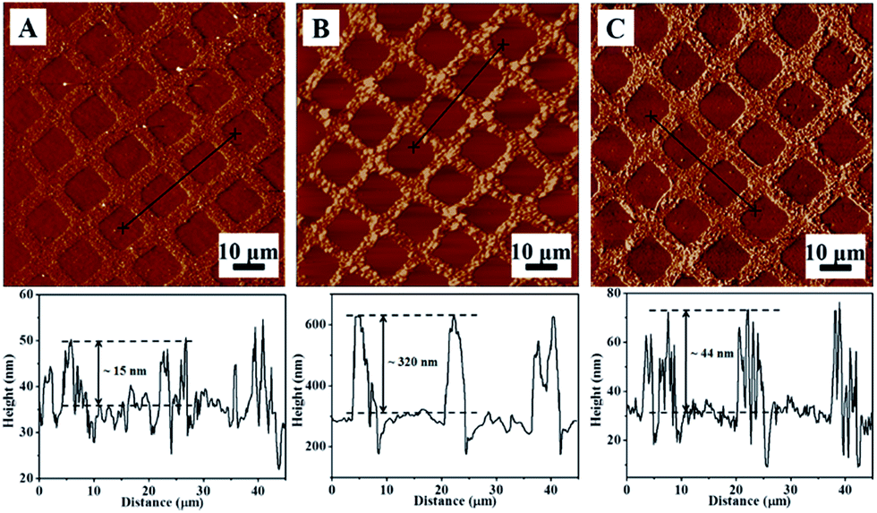 | ||
| Fig. 3 Tapping-mode AFM height images (90 μm × 90 μm) and the selected corresponding height profile of (A) patterned PDA film, (B) PS brushes grafted from the patterned PDA film and (C) PDMAEMA brushes grafted from the patterned PDA film. | ||
In order to verify the whether there was a successful polymerization process, water contact angle (CA) measurement was performed to investigate the surface properties of silicon substrate. Fig. 4A shows that the CA of the silicon substrate, treated with a fresh piranha solution, is ∼14°. After patterned modification with PDA, the value increases to ∼57°, indicating that the functional surface became less hydrophilic (Fig. 4B). The difference in surface wettability of the silicon substrate suggests a supramolecular structure of PDA. After subsequent amplification modification by PS brushes, the CA value rises to ∼94°, indicating significant hydrophobic properties of PS (Fig. 4C). After amplification modification by PDMAEMA brushes, the CA value decreases to ∼28°, and demonstrating crucial hydrophilic properties of PDMAEMA (Fig. 4D). Moreover, we also have measured advancing and receding contact angles by tilting plate method (Fig. S3†). The change of surface wettability before and after SIPGP indicated the success of polymerization.
 | ||
| Fig. 4 Static water contact angle measurements for (A) silicon wafer treated by fresh piranha solution. (B) Patterned PDA active surface on the silicon substrate. (C) PS brushes grafted from the patterned PDA coated silicon substrate. (D) PDMAEMA brushes grafted from the patterned PDA coated silicon substrate. | ||
Conclusions
In summary, biocompatible molecules of PDA has been successful used as the ink to construct micro-patterned PDA films on hydroxylated functionalized silicon wafer via the simple strategy of microcontact printing. Because of the multiple hydrogen bonds between PDA and silicon substrate and strong π–π stacking interactions among the PDA molecules, various PDA patterns (grid, ring, cubic) can be fabricated by tuning the concentration of PDA solution during μCP. Furthermore, the photoactive site on PDA surface could be amplified to grow polymer brushes via self-initiated photografting and photopolymerization, which endows the bio-inspired PDA films with various functionalities. Our patterning strategy in microcontact printing has the possibility to be extended to a wide range of polymers with special functional groups to form supramolecular interactions such as hydrogen bonds with substrates, which provide a robust and facile method to create patterned polymer films with tunable microstructures and could be used in surface based fields.Acknowledgements
This research was supported by the Chinese Academy of Science for Hundred Talents Program, the Chinese Central Government for Thousand Young Talents Program, the National Natural Science Foundation of China (51303195, 21304105), Ningbo Natural Science Foundation (2014A610127), Ningbo Science and Technology Bureau (2014B81010) and Excellent Youth Foundation of Zhejiang Province of China (LR14B040001).Notes and references
- H. Lee, S. M. Dellatore, W. M. Miller and P. B. Messersmith, Science, 2007, 318, 426 CrossRef CAS PubMed.
- X. Du, L. X. Li, J. S. Li, C. W. Yang, N. Frenkel, A. Welle, S. Heissler, A. Nefedov, M. Grunze and P. A. Levkin, Adv. Mater., 2014, 26, 8029 CrossRef CAS PubMed.
- Y. L. Liu, K. L. Ai and L. H. Lu, Chem. Rev., 2014, 114, 5057 CrossRef CAS PubMed.
- T. S. Sileika, H. D. Kim, P. Maniak and P. B. Messersmith, ACS Appl. Mater. Interfaces, 2011, 3, 4602 CAS.
- B. Zhao and W. J. Brittain, Prog. Polym. Sci., 2000, 25, 677 CrossRef CAS.
- T. Chen, I. Amin and R. Jordan, Chem. Soc. Rev., 2012, 41, 3280 RSC.
- N. Zhang, T. Pompe, I. Amin, R. Luxenhofer, C. Werner and R. Jordan, Macromol. Biosci., 2012, 12, 926 CrossRef CAS PubMed.
- H. W. Chien, W. H. Kuo, M. J. Wang, S. W. Tsai and W. B. Tsai, Langmuir, 2012, 28, 5775 CrossRef CAS PubMed.
- H. W. Chien and W. B. Tsai, Acta Biomater., 2012, 8, 3678 CrossRef CAS PubMed.
- M. Steenackers, S. Q. Lud, M. Niedermeier, P. Bruno, D. M. Gruen, P. Feulner, M. Stutzmann, J. A. Garrido and R. Jordan, J. Am. Chem. Soc., 2007, 129, 15655 CrossRef CAS PubMed.
- S. J. Ahn, M. Kaholek, W. K. Lee, B. LaMattina, T. H. LaBean and S. Zauscher, Adv. Mater., 2004, 16, 2141 CrossRef CAS PubMed.
- N. Ballav, S. Schilp and M. Zharnikov, Angew. Chem., Int. Ed., 2008, 47, 1421 CrossRef CAS PubMed.
- Y. N. Xia and G. M. Whitesides, Angew. Chem., Int. Ed., 1998, 37, 550 CrossRef CAS.
- F. Zhou, Z. J. Zheng, B. Yu, W. M. Liu and W. T. Huck, J. Am. Chem. Soc., 2006, 128, 16253 CrossRef CAS PubMed.
- Q. B. Wei, B. Yu, X. L. Wang and F. Zhou, Macromol. Rapid Commun., 2014, 35, 1046 CrossRef CAS PubMed.
- Z. H. Nie and E. Kumacheva, Nat. Mater., 2008, 7, 277 CrossRef CAS PubMed.
- P. Xiao, J. C. Gu, J. Chen, D. Han, J. W. Zhang, H. T. Cao, R. B. Xing, Y. C. Han, W. Q. Wang and T. Chen, Chem. Commun., 2013, 49, 11167 RSC.
- P. Xiao, J. C. Gu, J. Chen, J. W. Zhang, R. B. Xing, Y. C. Han, J. Fu, W. Q. Wang and T. Chen, Chem. Commun., 2014, 50, 7103 RSC.
- Y. H. Men, W. Q. Wang, P. Xiao, J. C. Gu, A. H. Sun, Y. J. Huang, J. W. Zhang and T. Chen, RSC Adv., 2015, 5, 31519 RSC.
- W. B. Sheng, B. Li, X. L. Wang, B. Dai, B. Yu, X. Jia and F. Zhou, Chem. Sci., 2015, 6, 2068 RSC.
Footnotes |
| † Electronic supplementary information (ESI) available. See DOI: 10.1039/c5ra10829b |
| ‡ These authors contribute equally to this work. |
| This journal is © The Royal Society of Chemistry 2015 |