Synthesis, structure and luminescence characteristics of a novel red phosphor NaLa9(GeO4)6O2:Eu3+ for light emitting diodes and field emission displays

Yaxin Cao, Ge Zhu and Yuhua Wang*
Key Laboratory for Special Function, Materials and Structural Design of the Ministry of Education, School of Physical Science and Technology, Lanzhou University, Lanzhou, 730000, China. E-mail: wyh@lzu.edu.cn; Fax: +86-931-8913554; Tel: +86-931-8912772

Received 2nd June 2015 , Accepted 27th July 2015

First published on 27th July 2015


Abstract

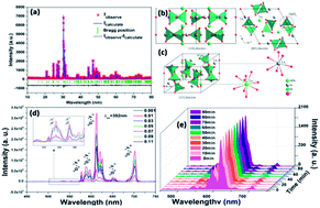
In order to explore a new kind of red phosphor for near ultraviolet white light emitting diodes (NUV-WLEDs) and field emission displays (FEDs), Eu3+ doped NaLa9(GeO4)6O2 was synthesized and its luminescence properties were studied for the first time for fundamental research. The results indicate that all samples crystallize in the hexagonal crystal system with the P63/m space group. Eu3+ doped NaLa9(GeO4)6O2 with the content of 0.07 has optimal photoluminescence properties, with a dominant red emission peak at 612 nm (5D07F2) with CIE coordinates of (0.64, 0.35) under 392 nm excitation and the quantum efficiency of 45.2%. Additionally, the thermal quenching property has been studied and its possible mechanism has also been expounded. Furthermore, the cathodoluminescence (CL) property was investigated and the result reveals that the sample has excellent degradation properties for FEDs. The study reveals that NaLa9(GeO4)6O2:0.07Eu3+ could be a suitable red-emitting phosphor candidate for NUV-WLEDs and FEDs.


1. Introduction

Over the past few years, white light emitting diodes (WLEDs) has become an interesting field for their many excellent characteristics, such as high efficiency, long lifetime, reliability, toxicity-free and energy-saving, etc.1–3 In recent years, LED technology has attracted much attention as a potential replacement for incandescent light sources.4,5 LEDs used for lighting are always formed with LED chips and one or several kinds of phosphors. By far, the most commonly used chips include blue LED chips and near ultraviolet (NUV) LED chips while desirable LED phosphors must possess strong absorption in the region of the LED chip's emission, high luminescence efficiency, excellent chemical and physical stability, low-cost and environmental friendliness.6 Conventional methods for generating white light using LEDs involve blending light from a blue LED chip with appropriate quantities of a yellow-emitting phosphor, such as cerium-doped yttrium aluminum garnet (YAG:Ce3+), on top of the blue LED chip.3,7,8 When the chip is driven under certain current, blue light is emitted by the InGaN chip through electron–hole recombination in the p–n junctions while some of it excites the YAG:Ce3+ phosphor to emit yellow light, and then the rest of the blue light would mix with the yellow light to generate white light. However, it suffers weakness of poor color rendering index (Ra < 80) because of the lack of red-light contribution, causing high color temperature.9–13 An alternative approach is to use an ultraviolet (UV)-LED to stimulate red-, green-, and blue-emitting (RGB) phosphors and NUV-LED chips could be more attractive. It might conquer the aforementioned pitfalls of the blue LED chip and on the other hand, NUV-LEDs are optically much more stable. It is considered that UV-LEDs might predominate solid-state-lighting (SSL) development for their high efficiency and easy fabrication.10 Until now, the blue and green phosphors, such as Ca5(PO4)3Cl:Eu2+, BaMgAl14O23:Eu2+/Mn2+, BaMgAl10O17:Eu2+/Mn2+, etc. are commercially available and could meet the requirements of NUV excitation in terms of spectra. However, we are suffering from lack of identified red phosphors for NUV-WLED application. There have been some reports on nitride-based and sulfide red phosphors, but Ce3+-, Eu2+-, or Mn2+-doped sulfide phosphors, however, suffer the problems of absorption of visible light and poor stability when exposed to air and high temperature. Additionally, it is also challengeable to make the nitride-based phosphors apply in industrialization for phosphor converted (pc)-WLEDs because the reported nitride based red phosphors will absorb not only the NUV lights but also the blue-green lights and they are excluded here because the absorption of visible light would decrease the total luminous efficiency.14,15 Therefore, much more effort is required to develop red phosphors. In this regard, researchers had paid more attention to oxide-based phosphors and some further research had been done to improve the luminescence properties, for example, using ligand passivant.16 Moreover, the FED is a promising candidate for the next generation of information display.17 For the realization of the full color FED, extensive research has been conducted to find new and more suitable FED phosphors. Standard sulfide phosphors, which have been studied for use in FED, however, are unstable under electron-beam bombardment, resulting in a chemical degradation of phosphor layer.18,19 In this respect, nonsulfide phosphors are desired in FED applications for improved stability, and many oxide phosphors have been investigated to escape the obstacles associated with degradation of sulfide phosphors.20–22 So it is also indispensable to search for phosphors that possess appropriate properties for FEDs.

Continuous attention has been paid to the discovery of rare-earth-activated silicate phosphors in a long run and recently, germanate phosphors has also been focused on, such as Mg3Y2Ge3O12:Ce3+ and Mg(F)GeO6:Mn2+.23 This is because Si and Ge elements are in the same fourth main group, namely, their outer electronic distributions are same. Their compound should be in the form of similar crystal structure and result in similar physical and chemical properties. Meanwhile, the difference of the electronegativities of Ge and O (ΔX = 1.43) is close to that of Si and O (ΔX = 1.54), so rare earth doped germanates could also have excellent optical properties.24 Among numerous of rare earth ions, Eu3+ is usually chosen as a typical and efficient activator for red emitting phosphor and its photoluminescence emission strongly depends on the symmetry of the crystal structure of the Eu3+-occupied site in the host. The optical transitions of Eu3+ ions originating from the electronic dipole and magnetic dipole interactions of the internal 4f electrons are affected by crystal environment seriously. If the Eu3+ ions occupy sites with inversion symmetry, emission peaks in the range of 590–600 nm from the 5D07F1 magnetic dipole transition will dominate the emission, which is not affected much by the site symmetry. On the contrary, the emission peaks around 610–630 nm from the 5D07F2 electronic dipole transition will dominate the emission if the Eu3+ ion substitutes a site with no inversion symmetry and this part will be notably affected by local asymmetry environment.25,26 However, the parity-forbidden nature of Eu3+ results in weak absorption cross section and thus low external quantum efficiency. There is one potential way to overcome this, to enhance the Eu3+ doping concentration. But it makes sense before the quenching concentration only.27,28 So it is necessary to find out the right concentration to obtain the optimal photoluminescence.

It is well known that apatite-type compounds have good luminescent properties. The luminescent properties of M+Ln9(SiO4)6O2 (M+ = Li, Na) and M22+Ln8(SiO4)6O2 (M2+ = Mg, Ca) activated by Eu3+ have been discussed by Blasse.29 According to report by Takahashi, an important structural characteristic of NaLa9Ge6O26 is that the La–La distances are quite large, i.e., 0.364 nm on nearest-neighbor sites and 0.40324(7) nm on the next-nearest neighbor sites.30 This fact elicits interest in the potential luminescent properties of this material, especially with respect to the phenomenon of concentration quenching. In this paper, the synthesis and crystal structure of the apatite, NaLa9(GeO4)6O2, is investigated and the luminescent properties of the Eu3+ doped NaLa9(GeO4)6O2 are studied for the first time. The photoluminescence and cathodoluminescence properties of the Eu3+ doped NaLa9(GeO4)6O2 are investigated which have shown that NaLa9(GeO4)6O2:Eu3+ could be a potential red-emitting phosphor for NUV-WLEDs and FEDs.

2. Experimental

2.1 Materials and synthesis

Samples of Eu3+ doped NaLa9(GeO4)6O2 were synthesized using a traditional solid-state reaction. Analytical reagents (AR) Na2CO3, La2O3, Eu2O3 and GeO2 (99.99%) were used as the starting materials. Stoichiometric amounts of the starting materials were firstly mixed into an agate mortar and ground substantially. Then the raw materials were put into a crucible and heated by a box-type furnace in air. The samples were firstly heated to 800 °C for 2 hours, and then further heated to 1380 °C for 5 hours, finally, the samples cooled slowly to room temperature.

2.2 Characterization

The crystal structure was identified using a Bruker D2 PHASER X-ray diffractometer (XRD) with graphite monochromator using Cu Kα radiation (λ = 1.54056 Å), operating at 30 kV and 15 mA and Fourier transform infrared spectroscopy (FTIR, Nicolet NEXUS 670). Reflectance spectra were measured on PE lambda950 UV-vis spectrophotometer using the BaSO4 white powder as the reference. The photoluminescence (PL) and photoluminescence excitation (PLE) spectra were obtained using a FLS-920T fluorescence spectrophotometer (Edinburgh Instruments) equipped with a 450 W Xe light source and double excitation monochromators. The PL decay curves were measured using an FLS-920T fluorescence spectrophotometer with an F900 nanosecond flash hydrogen lamp as the light source. High temperature luminescence intensity measurements were carried out using an aluminum plaque with cartridge heaters; the temperature was measured by thermocouples inside the plaque and controlled with a standard TAP-02 high temperature fluorescence controller (Orient KOJI instrument Co., Ltd). The CL properties of the samples were obtained using a modified Mp-Micro-S instrument (Horiba Jobin Yvon).

3. Results and discussion

3.1 Study on phase identification and crystal structure

A series of different concentration of Eu3+ doped NaLa9(GeO4)6O2:xEu3+ (0 ≤ x ≤ 0.11) have been synthesized. The XRD results are shown in Fig. 1a. It indicates that the peaks have a shift to a higher angle area when increase the concentration of Eu3+ ion. The radius of six-, seven-, nine-fold coordinated Eu3+ is 0.947 Å, 1.01 Å and 1.120 Å, respectively while the radius of six-, seven-, nine-fold coordinated La3+ is 1.032 Å, 1.10 Å and 1.216 Å, respectively.31 According to Bragg equation (2d[thin space (1/6-em)]sin[thin space (1/6-em)]θ = λ), when Eu3+ substitutes La3+ in the crystal site, it could cause a lattice distortion which will make a smaller d and a larger θ should express due to this. The experimental result fit Wegener's rules well and it also indicated that Eu3+ ion has been embedded in the host lattice well.
image file: c5ra10435a-f1.tif
Fig. 1 (a) XRD patterns of different concentrations of Eu3+ doped samples, the right part shows patterns from 29.6 to 31.15° in detail; (b) XRD refinement result of NaLa9(GeO4)6O2:0.07Eu3+; (c) the different lattice parameters as a function of Eu3+ concentrations; (d) the structural views of NaLa9(GeO4)6O2:0.07Eu3+ along [110], [001] direction, respectively and (e) a structural view of NaLa9(GeO4)6O2:0.07Eu3+ in the direction of [12[1 with combining macron]] and coordination environments for all independent metal atoms in NaLa9(GeO4)6O2:0.07Eu3+.

Fig. 1b shows structural refinements of the XRD patterns of NaLa9(GeO4)6O2:0.07Eu3+ compound as a typical sample. The pink crosses and blue solid lines depict the observed and calculated patterns, respectively. The green short vertical lines show the position of Bragg reflections of the calculated patterns. The difference between the experimental and calculated patterns is plotted by black line at the bottom. The structure parameters reported on NaLa9(GeO4)6O2 were used as initial parameters in the Rietveld analysis.32 The refined results of NaLa9(GeO4)6O2 are summarized in Table 1. The residual factors are Rwp = 8.15%, and Rp = 6.19%. The results indicate that the powder sample is crystallized in hexagonal symmetry with space group P63/m. The lattice parameters of NaLa9(GeO4)6O2:0.07Eu3+ are a = 9.862(0) Å and c = 7.234(5) Å, respectively. Furthermore, the lattice parameters of different concentration of Eu3+ doped samples were calculated and the relationship between concentration and parameters are shown in Fig. 1c. These results indicate that the lattice parameters decreased with increasing Eu3+ concentration with a linear relation. This is because when Eu3+ is doped, the host lattice would have a contraction due to its smaller ionic radius, and the more Eu3+ is doped, the severer the contraction would be.

Table 1 The refined unit cell parameters and residual factors
Atom Ox. Wyck. x/a y/b z/c Ueq
La1 3 4f 1/3 2/3 0.0003(2) 0.01629
Na1 1 4f 1/3 2/3 0.0003(2) 0.01629
La2 3 6h 0.24157(4) 0.01251(4) 1/4 0.01612
Ge1 4 6h 0.37346(7) 0.40143(7) 1/4 0.01299
O1 −2 6h 0.4867(6) 0.3121(6) 1/4 0.12412
O2 −2 6h 0.5234(6) 0.3961(5) 3/4 0.13668
O3 −2 12i 0.2468(4) 0.3407(6) 0.4396(5) 0.08165
O4 −2 2a 0 0 1/4 0.05385


According to the refinement results, in NaLa9(GeO4)6O2 structure, there are 42 crystallographically independent atoms in the unit cell, including 1 Na, 9 La, 6 Ge and 26 O atoms. Fig. 1d shows the projections of the structures of NaLa9(GeO4)6O2 along [110] and [001] directions. As shown in Fig. 1e, the crystal structure of NaLa9(GeO4)6O2 is a three-dimensional framework consisting of LaO7, LaO9, GeO4 and NaO9 polyhedra. In order to afford clear views of the structure, only GeO4 (dark green part) is presented as polyhedron in Fig. 1d and e. The view from [001] direction clearly shows that the GeO4 tetrahedra form polyhedra rings around the c-axis to form layers stacking induces tunnels parallel to the c-axis with large cavities in which the La or Na atoms are located, with seven and nine coordinations. Fig. 1e clearly shows the coordination environment of La (including La1 and La2) and Na (the same as La1) atoms in NaLa9(GeO4)6O2. La1 (Na) in the 4f site coordinates with nine O atoms of which the O atoms are from GeO4 tetrahedra only. La2 in the 6h site coordinates with seven O atoms including six from GeO4 tetrahedra and one in the tunnel. The two different La positions of La1 and La2 are located in GeO4 coordination polyhedra. Based on the effective ionic radius and the similar electric charge, when Eu3+ enter into the lattice matrix, they are expected to randomly enter into La3+ sites and experience specific local asymmetry environment, that is, the La1 site and La2 site, both are inversion symmetry sites.

The FTIR spectrum of the as-prepared material is shown in Fig. 2a. The absorption at 3433.3 cm−1 and 1628.2 cm−1 can be attributed to O–H vibrations (stretching and bending, respectively) of the adsorbed water on the surface of the phosphors. It also displays several characteristic absorptions around 746.4, 477.1 cm−1 which are attributed to Ge–O vibration.33


image file: c5ra10435a-f2.tif
Fig. 2 (a) FITR spectrum of NaLa9(GeO4)6O2, and (b) DRS of the matrix and NaLa9(GeO4)6O2:0.07Eu3+, the inset shows the determined band gap of NaLa9(GeO4)6O2 being 3.11 eV.

Diffuse reflectance spectra (DRS) of the matrix and 0.03 Eu3+ doped samples are shown in Fig. 2b. A broad band is observed in the spectrum of the matrix before 350 nm. For the 0.03 Eu3+ doped sample, the broad band can be attributed to Eu3+–O2− charge transition (CT) and two small peaks at 392 and 462 nm are related to 7F05L6 and 7F05D2 transition, respectively. These optical absorptions are due to the excitation of electrons from valence band (VB) to conductive band (CB). Although an exact discussion of transitions from VB to CB requires calculation of the excited state electronic structure, the calculated static electronic band, as an approximation, may still provide important information. The calculated band structure shown in Fig. 3 reveals that NaLa9(GeO4)6O2:Eu is a direct band gap material. The calculated direct band gap Eg is 3.54 eV. The band gap can be also calculated by the Kubelka–Munk equation.34

 
F(R) = (1 − R)1/2/2R = k/s (1)
where R is the diffuse reflectance of the layer relative to standard, k is the molar absorption coefficient of the sample and s is the scattering coefficient. According to the relationship between diffuse reflectance R and energy E shown in the inset diagram in Fig. 2b, the F(R) as a function of E can be obtained, and the intersection between the linear fit of F(R) and the photon energy (wavelength) axis gives the value of the band gap.35 The band gap of NaLa9(GeO4)6O2 was determined to be 3.11 eV (398 nm) through the F(R)-energy relation graph. The calculated band gap values are similar through the two methods. The inconsistency comes mainly from errors of correlation function calculations, slightly from the errors introduced from the measurement of the DRS and the estimation by using eqn (1).


image file: c5ra10435a-f3.tif
Fig. 3 Calculated band structures (left) and DOS (right) of hexagonal NaLa9(GeO4)6O2 near the Fermi energy level (the red dash below). The Fermi energy is the zero of the energy scale. Eg is the calculated forbidden band gap of the ground state of the system.

3.2 Photoluminescence properties of Eu3+ doped NaLa9(GeO4)6O2

The PLE spectra of NaLa9(GeO4)6O2:xEu3+ (0.001 ≤ x ≤ 0.11) samples monitoring at 612 nm shown in Fig. 4a consist of a broad band centered at around 300 nm and several sharp peaks ranging from 350 to 500 nm. The band excitation can be assigned to the charge transition band (CTB), resulting from an electron transfer from the ligand O2− (2P6) orbital to the empty state of 4f6 in the Eu3+ ion (Eu3+–O2−) and it contains a small peak at 317 nm that corresponds to7F05HJ transition. The latter line peaks should relate to the characteristic 4f–4f transitions of Eu3+ ions; those correspond to the transitions from the ground state 7F0 to the excited levels 5D4 (361 nm), 5L7, 5GJ (375 nm, 380 nm), 5L6 (392 nm), 5D3 (412 nm) and 5D2 (462 nm) of Eu3+. Phosphors for NUV-LEDs should have strong absorption around 400 nm (emission wavelength of NUV-LED chips). Obviously, the PLE spectra show strong absorption around 400 nm (392 nm), indicating that the phosphor can be a candidate for red-emitting phosphors for NUV-LEDs.
image file: c5ra10435a-f4.tif
Fig. 4 (a) The PLE spectra of samples with Eu3+ concentrations from 0.001 to 0.11; (b) PL spectra of all the samples (the inset shows the magnified part reveals the transitions from higher 5D1 energy); (c) diagram of concentration affected asymmetry ratio and relative intensity and (d) photoluminescence comparison of commercial phosphor and NaLa9(GeO4)6O2:0.07Eu3+.

Fig. 4b shows the emission spectra of the series phosphors under 392 nm excitation. The spectra consist of a number of sharp lines mainly ranging from 450 to 750 nm, which peaked at 578 nm (5D07F0), 588 nm (5D07F1), 612 nm (5D07F2), 650 nm (5D07F3) and 701 nm (5D07F4), respectively. The inset shows the transitions from higher 5D1 state, peaking at 535 nm (5D17F1) and 553 nm (5D17F2). The line shape of the emission almost does not change with the variation of Eu3+ concentration because most of the valence electrons of trivalent rare-earth elements are shielded by 5s and 5p outer electrons, and the f–f transitions of trivalent lanthanides are weakly affected by ligand ions in the crystals.3 For Eu3+, the relative intensity of 5D07FJ multiplet emission is also an important factor that determines the chromaticity or saturation of red color; in general, the larger the magnitude of ((5D07F2)/(5D07F1)) (R/O), the closer to the optimal value of the color chromaticity. On the other hand, R/O ratio can also perform as the asymmetry ratio, which suggests the degree of distortion.36,37 In this study, we observed that the R/O ratio increase with increasing x value. As shown in Fig. 4c, the asymmetry ratio increases as the concentration of Eu3+ ions increases. This is because when Eu3+ ions were doped, it could cause distortion of the host lattice and the more Eu3+ ions are, the fiercer would the distortion be. The intensity of transition 5D07F2 would be more sensitive to the coming distortion than 5D07F1, as a result, the R/O ratio increases. The PL intensity is found to increase with increasing Eu3+ concentration before 0.07, and after that, intensity decreases and this is attributed to a concentration-quenching effect as shown in Fig. 4a and b. The comparison of PL property between commercial phosphor Y2O3:Eu3+ and synthesized NaLa9(GeO4)6O2:0.07Eu3+ in Fig. 4d shows that the latter has broader emission lines which results in a larger integral area, which indicates that the synthesized NaLa9(GeO4)6O2:0.07Eu3+ have a higher brightness than the commercial phosphor. It is well know that quantum efficiency is very important when it comes to real application. Normally, Eu3+ shows relatively high internal quantum efficiency in solids at low concentration. The higher concentration could give a higher external quantum efficiency but quench the Eu3+ PL in NaLa9(GeO4)6O2.38,39 We measured the quantum efficiency of NaLa9(GeO4)6O2:0.07Eu3+ which has the heaviest doping amount but doesn't quench to be 45.2%.

The temperature stability of optical properties is important for evaluating luminescent materials, since the luminescent materials may suffer from high temperature during long-term operation.40 Fig. 5a shows the luminescence intensity of NaLa9(GeO4)6O2:0.07Eu3+ at different temperature when excited at 392 nm. It indicates that the PL intensity decreases with the increasing temperature in an approximate liner manner (shown in the inset of Fig. 5a) which reveals that the phosphor may have potential to be used for a temperature sensor. The luminescence thermal quenching effect is usually attributed to the nonradiative relaxation through the crossing point between the excited state and the ground state in the configurational coordinate diagram.41 Fig. 5b shows the possible mechanism of thermal quenching. When there is irradiation, electrons on the ground state would be excited to the excited states and then emits photons while back to the ground state. Firstly, electrons are excited to 5D0 and 5D1 states. Generally, the electrons on 5D1 state can cross-relaxing to the 5D0 state and then the electrons could return to the ground states through pathway of the thermal quenching which is related to the 5D0 state and Eu3+–O2− CTB: some electrons overcome the activation energy ΔE assisted by phonons as the temperature increases and then feed to the 7FJ state, which provides the nonradiative process (via (3)), and on the other hand, the remaining electrons contribute to the 5D07F2 emission at 612 nm (via (1)). A few of the electrons excited to 5D1 state return to the ground state directly which cause the emission 5D17FJ (J = 1, 2) (via (2)), the emission could be very weak due to the small transition odds.


image file: c5ra10435a-f5.tif
Fig. 5 (a) The temperature dependent emission spectra of the NaLa9(GeO4)6O2:0.07Eu3+ phosphor. The inset shows temperature dependent peak values of the sample; (b) the schematic illustration of a configurational coordinate diagram of the thermal quenching process in Eu3+ doped NaLa9(GeO4)6O2 and (c) the calculated activation energy for thermal quenching of the NaLa9(GeO4)6O2:0.07Eu3+ phosphor.

The nonradiative transition probability is strongly dependent on temperature resulting in the decrease of emission intensity. The temperature dependence of the emission intensities of phosphors could be described according to the following modified Arrhenius equation:42

 
I(T) = I0[1 + A[thin space (1/6-em)]exp(−ΔE/kT)]−1 (2)
where I(T) is the intensity at a given temperature, I0 is the initial intensity, k is the Boltzmann constant, T is the temperature, and ΔE is the activation energy from the 5D0 state to the CTB and can be regarded as a constant because the shape of the emission curve did not change significantly. Based on eqn (2), we can plot ln[(I0/I) − 1] vs. 1/kT yielding a straight line, and the activation energy ΔE is obtained from the slop of the plot. As shown in Fig. 5c, the experimentally calculated activation energy ΔE was 0.279 eV for NaLa9(GeO4)6O2:0.07Eu3+.

Fig. 6a shows the luminescence decay curves of the phosphor NaLa9(GeO4)6O2:xEu3+ excited at 392 nm and monitored at 612 nm. All the curves can be well fitted by an exponential function and the lifetime value can be given to the average lifetime defined as:43,44

 
τaverage = ∫tI(t)dt/∫I(t)dt (3)


image file: c5ra10435a-f6.tif
Fig. 6 (a) Decay curves of different concentrations of Eu3+ (from 0.001 to 0.11) doped samples when excited at 392 nm and (b) 0.07 Eu3+ doped sample monitoring under different wavelength of 553, 588, 612, 701 nm when excited at 392 nm.

For 5D07F2 (612 nm) of Eu3+ ions, the lifetimes vary from 1.316 to 1.438 ms for different concentrations. The lifetime becomes shorter gradually when increasing the concentration of Eu3+. For 5D17F1 (553 nm), 5D07F1 (588 nm), 5D07F2 (612 nm) and 5D07F4 (701 nm), the average lifetimes are 0.716, 1.387, 1.328 and 1.379 ms, respectively, which is shown in Fig. 6b. From the lifetimes, it can be found that the lifetime of the higher energy level (5D1) emission is shorter than that of the lower energy (5D0) emission. This is because the higher energy level is more metastable than the lower energy level, and the electron at the higher energy level would like to either transition to the ground (7FJ, J = 1, 2, 3, 4) state or relax to the low energy level nonradiatively by multiphonon emission.45 Thus, the luminescence decay curve can also be used to distinguish the lower level 5D0 with upper levels of Eu3+, such as 5D1, 5D2 or 5D3.

3.3 Cathodoluminescence properties of Eu3+ ions in NaLa9(GeO4)6O2

The CL properties of the sample NaLa9(GeO4)6O2:0.07Eu3+ have been investigated to explore their potentials in the development of efficient red phosphors for FED systems. For cathodoluminescence, the Eu3+ ions are excited by the plasma produced by the incident electrons. The CL spectrum of NaLa9(GeO4)6O2:0.07Eu3+ consists of several characteristic emission lines of Eu3+, peaking at 536 nm, 557 nm, 591 nm, 615 nm, 655 nm and 705 nm, respectively. Compared with its PL spectrum, the prominent emission becomes broader and exhibits a little red shift of 1–4 nm. This phenomenon may due to the energy level structures of vacancy defects and a different excitation mechanism.46 The CL emission intensities for the samples NaLa9(GeO4)6O2:0.07Eu3+ have been investigated as a function of accelerating voltage and filament current, respectively, which are shown in Fig. 7a and b, respectively. When the filament current is given as 80 mA, the CL intensity gradually increases with applied voltage from 3.0 to 10.0 kV (Fig. 7a). And when it is excited under a voltage of 8.0 kV, the CL intensity also increases with increasing of the filament current from 10 to 100 mA (Fig. 7b). It can be interpreted that with the increase of accelerating voltage or filament current, more plasma is produced, which results in more ions being excited and thus the CL intensity increases.47 The increase in CL brightness with an increase in the electron energy and filament current is attributed to the deeper penetration of the electrons into the phosphor body and the larger electron beam current density.47,48
image file: c5ra10435a-f7.tif
Fig. 7 Cathodoluminescence properties of NaLa9(GeO4)6O2:0.07Eu3+ (a) with a constant filament current 80 mA (the inset shows the voltage related CL intensity) and (b) under a constant voltage 8.0 kV (the inset shows the current related CL intensity).

The degradation property of phosphors is very important for FED application. In general, the use of phosphors with poor efficiency at low voltage leads to the need for high current operation which enhances the phosphor degradation. And for most phosphors used in FEDs, the CL intensity decreased with the increase of the bombing times. This is because during continuous electron bombardment, graphitic carbon will accumulate on the surface of phosphors and cause the well-known effect of carbon contamination, which will exacerbate surface charging, and thus lower the CL intensity.49 Thus we tried to investigate the degradation behavior of NaLa9(GeO4)6O2:0.07Eu3+ sample under continuous low-voltage electron-beam excitation and this is showed in Fig. 8a. The accelerating voltage was kept at 8.0 kV and the filament current was 50 mA. As it shows that the CL intensity of NaLa9(GeO4)6O2:0.07Eu3+ almost keep constant under a continuous electron bombardment which indicates that the synthesized phosphor could keep wonderful stability when used for FEDs. For comparison, the degradation property of the commercial Y2O3:Eu3+ was also measured and their comparison result is shown in Fig. 8b. It is obvious that degradation property of the synthesized NaLa9(GeO4)6O2:0.07Eu3+ is better than that of Y2O3:Eu3+.


image file: c5ra10435a-f8.tif
Fig. 8 (a) Degradation property of NaLa9(GeO4)6O2:0.07Eu3+ and (b) time dependence intensity compared with Y2O3:Eu3+.

4. Conclusion

In this work, a novel red-emitting phosphor NaLa9(GeO4)6O2:xEu3+ has been successfully synthesized, while the structure and luminescence properties were investigated in detail. The results indicate that the sample NaLa9(GeO4)6O2:0.07Eu3+ has optimal luminescence properties. Photoluminescence property of the synthesized NaLa9(GeO4)6O2:0.07Eu3+ has been compared with Y2O3:Eu3+ when under 392 nm excitation, which suggests that the former performs excellent lightness. It can be also found that NaLa9(GeO4)6O2:0.07Eu3+ phosphor shows the bright red emission of Eu3+ 5D07F2 transitions and it performed an excellent degradation property under continuous low-voltage electron-beam excitation through its CL spectrum. Therefore, the NaLa9(GeO4)6O2:0.07Eu3+ with excellent photoluminescence and cathodoluminescence could be a promising candidate for NUV-WLEDs and FEDs.

Acknowledgements

This work was supported by Specialized Research Fund for the Doctoral Program of Higher Education (No. 20120211130003) 35, the National Science Foundation for Distinguished Young Scholars (No. 50925206) and the Gansu Province Development and Reform Commission.

References

  1. E. F. Schubert and J. K. Kim, Science, 2005, 308, 1274 CrossRef CAS PubMed.
  2. S. Nakamura, T. Mukai and M. Senoh, Appl. Phys. Lett., 1994, 64, 1687 CrossRef CAS PubMed.
  3. S. Ye, F. Xiao, Y. X. Pan, Y. Y. Ma and Q. Y. Zhang, Mater. Sci. Eng., R, 2010, 71, 1 CrossRef PubMed.
  4. Y. Shimizu, K. Sakano, Y. Noguchi and T. Moriguchi, US Pat. 5, 1998, vol. 998, p. 925.
  5. K. Sakuma, N. Hirosaki, N. Kimura, M. Ohashi, R. J. Xie, Y. Yamamoto, T. Suehiro, K. Asano and D. Tanaka, IEICE Trans. Electron., 2005, E88-C, 2057 CrossRef.
  6. X. Y. Huang, Nat. Photonics, 2014, 8, 748 CrossRef CAS PubMed.
  7. H. A. Hoppe, Angew. Chem., Int. Ed., 2009, 48, 3572 CrossRef PubMed.
  8. C. Feldmann, T. Justel, C. R. Ronda and P. J. Schmidt, Adv. Funct. Mater., 2003, 13, 511 CrossRef CAS PubMed.
  9. D. A. Steigerwald, J. C. Bhat, D. Collins, R. M. Fletcher, M. O. Holcomb, M. J. Ludowise, P. S. Martin and S. L. Rudaz, IEEE J. Sel. Top. Quantum Electron., 2002, 8, 310 CrossRef CAS.
  10. J. K. Sheu, S. J. Chang, C. H. Kuo, Y. K. Su, L. W. Wu, Y. C. Lin, W. C. Lai, J. M. Tsai, G. C. Chi and R. K. Wu, IEEE Photonics Technol. Lett., 2003, 15, 18 CrossRef.
  11. M. S. Shur and A. Zukauskas, Proc. IEEE, 2005, 93, 1691 CrossRef CAS.
  12. M. R. Krames, O. B. Shchekin, R. Mueller-Mach, G. O. Mueller, L. Zhou, G. Harbers and M. G. Craford, J. Disp. Technol., 2007, 3, 160 CrossRef CAS.
  13. M. Yamada, Y. Narukawa, H. Tamaki, Y. Murazaki and T. Mukai, IEICE Trans. Electron., 2005, E88C, 1860 CrossRef.
  14. R. J. Xie and N. Hirosaki, Sci. Technol. Adv. Mater., 2007, 8, 588 CrossRef CAS PubMed.
  15. X. H. He, N. Lian, J. H. Sun and M. Y. Guan, J. Mater. Sci., 2009, 44, 4763 CrossRef CAS.
  16. Q. L. Dai, M. E. Foley, C. J. Breshike, A. Lita and G. F. Strouse, J. Am. Chem. Soc., 2011, 133, 15475 CrossRef CAS PubMed.
  17. L. E. Shea, Electrochem. Soc. Interface, 1998, 24 CAS.
  18. J. Ballato, J. S. Lewis and P. H. Holloway, Mater. Res. Soc. Bull., 1999, 24, 51 CAS.
  19. H. C. Swart, T. A. Trottier, J. S. Sebastian, S. L. Jones and P. H. Holloway, J. Appl. Phys., 1998, 83, 4578 CrossRef CAS PubMed.
  20. S. S. Chadha, D. W. Smith, A. Vecht and C. Gibbons, SID Int. Symp. Dig. Tech. Pap., 1994, 25, 51 Search PubMed.
  21. S. H. Cho, J. S. Yoo and J. D. Lee, J. Electrochem. Soc., 1996, 143, L231 CrossRef CAS PubMed.
  22. S. Itoh, H. Toki, K. Tamura and F. Kataoka, Jpn. J. Appl. Phys., 1999, 31, 6387 CrossRef.
  23. C. W. Meyer, D. C. Meier, C. B. Montgomery and S. Semancik, Sens. Actuators, A, 2006, 127, 235 CrossRef CAS PubMed.
  24. M. D. Que, Z. P. Ci, Y. H. Wang, G. Zhu, B. T. Liu, J. Zhang, Y. R. Shi, Y. Wen, Y. Li and Q. Wang, J. Am. Ceram. Soc., 2012, 1 Search PubMed.
  25. G. Blasse, Prog. Solid State Chem., 1988, 18, 79 CrossRef CAS.
  26. J. Feng and H. J. Zhang, Chem. Soc. Rev., 2013, 42, 387 RSC.
  27. G. J. Gao, S. Reibstein, M. Y. Peng and L. Wondraczek, J. Mater. Chem., 2011, 21, 3156 RSC.
  28. G. J. Gao, J. X. Wei, Y. Shen, M. Y. Peng and L. Wondraczek, Opt. Mater. Express, 2014, 4, 476 CrossRef CAS.
  29. G. Blasse, J. Solid State Chem., 1975, 14, 181 CrossRef CAS.
  30. M. Takahashi, K. Uematsu, Z. G. Ye and M. Sato, J. Solid State Chem., 1998, 139, 304 CrossRef CAS.
  31. R. D. Shannon, Acta Crystallogr., Sect. A: Cryst. Phys., Diffr., Theor. Gen. Crystallogr., 1976, 32, 751 CrossRef.
  32. J. M. Phillips, et al., Laser Photonics Rev., 2007, 1, 307 CrossRef CAS PubMed.
  33. V. G. Zubkov, I. I. Leonidov, A. P. Tyutyunnik, N. V. Tarakina, I. V. Baklanova, L. A. Perelyaeva and L. L. Surat, Phys. Solid State, 2008, 50, 1699 CrossRef CAS.
  34. P. Kubelka, J. Opt. Soc. Am., 1948, 38, 448 CrossRef CAS.
  35. S. P. Tandon and J. P. Gupta, Phys. Status Solidi B, 1970, 38, 363 CrossRef CAS PubMed.
  36. S. Fujihara and K. Tokumo, Chem. Mater., 2005, 17, 5587 CrossRef CAS.
  37. H. S. Yoo, W. B. Im, S. W. Kim, B. H. Kwon and D. Y. Jeon, J. Lumin., 2010, 130, 153 CrossRef CAS PubMed.
  38. G. J. Gao, J. X. Wei, Y. Shen, M. Y. Peng and L. Wondraczek, J. Mater. Chem. C, 2014, 2, 8678 RSC.
  39. G. J. Gao and L. Wondraczek, J. Mater. Chem. C, 2014, 2, 691 RSC.
  40. Y. Tian, B. J. Chen, R. N. Hua, N. S. Yu, B. Q. Liu, J. S. Sun, L. H. Cheng, H. Y. Zhong, X. P. Li, J. S. Zhang, B. N. Tian and H. Zhong, CrystEngComm, 2012, 14, 1760 RSC.
  41. R. A. Hansel, S. W. Allison and D. G. Walker, Appl. Phys. Lett., 2009, 95, 114102 CrossRef PubMed.
  42. H. S. Jang, H. Y. Kim, Y. S. Kim, H. M. Lee and D. Y. Jeon, Opt. Express, 2012, 20, 2761 CrossRef CAS PubMed.
  43. F. P. Du, Y. Nakai, T. Tsuboi, Y. Huang and H. J. Seo, J. Mater. Chem., 2011, 21, 4669 RSC.
  44. Y. Tian, B. J. Chen, R. N. Hua, J. S. Sun, L. H. Cheng, H. Y. Zhong, X. P. Li, J. S. Zhang, Y. F. Zheng, T. T. Yu, L. B. Huang and H. Q. Yu, J. Appl. Phys., 2011, 109, 053511 CrossRef PubMed.
  45. X. Liu, C. Li, Z. Quan, Z. Cheng and J. Lin, J. Phys. Chem. C, 2007, 111, 16601 CAS.
  46. X. M. Liu and J. Lin, J. Mater. Chem., 2008, 18, 221 RSC.
  47. Z. H. Xu, X. J. Kang, C. X. Li, Z. Y. Hou, C. M. Zhang, D. M. Yang, G. G. Li and J. Li, Inorg. Chem., 2010, 49, 6706 CrossRef CAS PubMed.
  48. Y. Zhang, G. G. Li, D. L. Geng, M. M. Shang, C. Peng and J. Lin, Inorg. Chem., 2012, 51(21), 11655 CrossRef CAS PubMed.
  49. J. J. Hren, in Principles of Analytical Electron Microscopy, ed. D. C. Joy, A. D. Romig and J. I. Goldstein, Plenum, New York, 1986, p. 353 Search PubMed.

This journal is © The Royal Society of Chemistry 2015
Click here to see how this site uses Cookies. View our privacy policy here.