
A monolithic integration of robust, water-/oil-repellent layer onto multilayer encapsulation films for organic electronic devices†
Shin Young Kim‡
,
Bong Jun Kim‡,
Do Heung Kim and
Sung Gap Im*
Department of Chemical and Biomolecular Engineering and KI for the NanoCentury, Korea Advanced Institute of Science and Technology (KAIST), Daejeon, Republic of Korea 305-701. E-mail: sgim@kaist.ac.kr; Tel: +82-42-350-3936
First published on 7th August 2015
Abstract
A robust, water-/oil-repellent surface layer was integrated monolithically onto a multilayer thin film encapsulation by a sequential deposition of poly(2,4,6,8-tetravinyl-2,4,6,8-tetramethylcyclotetrasiloxane) followed by poly(3,3,4,4,5,5,6,6,7,7,8,8,9,9,10,10,10-heptadecafluorodecyl methacrylate) via a solvent-free initiated chemical vapor deposition method. The fabrication process did not damage the encapsulation performance of the underlying barrier films. Due to the low surface energy coupled with the uniform nano-structure of the poly(3,3,4,4,5,5,6,6,7,7,8,8,9,9,10,10,10-heptadecafluorodecyl methacrylate) layer, the outermost hydrophobic layer on the multilayer thin film encapsulation showed an excellent water-/oil-repellency, with water and hexadecane contact angles of 121.9 ± 4.9° and 75.3 ± 4.7°, respectively. This endowed a substantially improved self-cleaning performance to the multilayer thin film encapsulation. With two dyads of alternating poly(2,4,6,8-tetravinyl-2,4,6,8-tetramethylcyclotetrasiloxane)/Al2O3 hybrid multilayer integrated with the self-cleaning layer, the water vapor transmission rate value of 2.3 ± 1.1 × 10⁻³ g m−2 d−1 was achieved under accelerated condition at 38 °C with the relative humidity of 90%. This value corresponds to 1.1 × 10⁻⁴ g m−2 d−1 under ambient condition at 25 °C with the relative humidity of 50%. In addition, the film showed the high transmittance of 92.5% in the visible spectrum. The total thickness of the water-/oil-repellent thin film encapsulation layer was only 1.3 μm, which is highly desirable for ultrathin future flexible electronic devices.
1. Introduction
Organic photovoltaics (OPVs) have attracted great interest from both academia and industry due to their extraordinary advantageous characteristics, such as high flexibility, low fabrication cost, light weight, and scalability.1,2 Since OPV device efficiency is low compared to silicon-based devices, considerable research efforts have been made to improve their performance.3,4 In addition to low efficiency, another critical obstacle to their commercialization is their short lifetime. The problem mainly originates from two factors: the vulnerability of the organic layer and metal when exposed to moisture and/or oxygen,5 and the surface contamination of the device by various types of environmental contaminants such as dust, particles, water and oil stains, which significantly block the absorption of the incident light.6,7 Unlike other electronic applications, OPVs will primarily be deployed in an outdoor environment, and fouling of the OPV surface is a significant factor affecting device efficiency. Consequently, these two problems must be resolved, to extend OPV lifetime, and thus stimulate the commercialization of the device.Various encapsulation methods have been proposed since the development of organic electronics to prevent the penetration of moisture and oxygen into the devices. In particular, over the last decade, thin film encapsulation (TFE) systems consisting of organic/inorganic multilayers have been exploited intensively, since they can provide outstanding flexibility as well as excellent barrier properties.8,9 However, most of the current researches focused on decreasing the water vapor transmission rate (WVTR) of the developed TFE by introducing new organic/inorganic materials, and by engineering the configuration of the inorganic/organic TFE. For example, the barrier properties of Al2O3-based TFE were improved by laminating the Al2O3 layer with TiO2 or ZrO2.10,11 A new organosilicon-based organic layer material was adopted to improve barrier properties.12 The dyad number and thickness of an organic/inorganic multilayer were also varied to achieve the maximum barrier properties as well as flexibility.13,14 The surface properties of the TFE were often disregarded, and the anti-contamination researches were conducted separately.
To minimize contamination of the device surface, anti-contamination surfaces have also been investigated as a protective layer.15,16 For example, increasing the surface roughness of the protective layer through the use of UV exposure or post-thermal treatment has been attempted in efforts to lower the surface energy of the substrates.17,18 However, these methods commonly caused damage to the substrates, and often limited their application on the surface of organic electronic devices.5,19 Hydrophobic layers such as fluoroalkylsilane-based self-assembled monolayer (SAM) and Cytop™ polymer films have also been spun on the substrates as protective layers, but the coating process required an organic solvent and a thermal annealing process greater than 100 °C which also cannot be applied directly to organic electronic devices.20,21 Similarly, a hydrophobic magnesium fluoride (MgF2) layer was deposited by thermal evaporation as a protective layer on an encapsulation layer.22
In summary, although there have been various approaches, so far most of the studies related to providing water repellency have required the use of harsh process conditions, or organic solvents which are damaging to organic electronic devices. A process to directly apply a flexible, high-performance encapsulation layer with anti-contamination properties to organic electronic devices without damaging them has not yet been demonstrated.
Here, we adopted atomic layer deposition (ALD), and initiated chemical vapor deposition (iCVD) processes to fabricate a multilayer TFE system with anti-contamination properties. The organic and inorganic layers of the multilayer were deposited via iCVD and ALD, respectively. ALD is a layer-by-layer deposition method using a binary reaction with precursors, which offers highly dense films of atomic scales at relatively low temperature.23 Due to its self-limiting reaction on the surface, an ultra-thin (<100 nm) film can be prepared with precise thickness control. iCVD is a solvent-free process, where a radical polymerization occurs in vapor phase, resulting in various functional polymer films.24 In previous studies, it has been confirmed that the pinhole-free, conformal nature of the iCVD process enabled the formation of an excellent interface with inorganic layers.25–27 For that purpose, the combination of iCVD-ALD processes provided an effective method of fabricating excellent encapsulation film composed of hybrid organic/inorganic multilayer.28 In that work, poly(2,4,6,8-tetravinyl-2,4,6,8-tetramethylcyclotetrasiloxane) (pV4D4) film deposited via the iCVD process, and Al2O3 deposited via the ALD process, were used as an organic layer and an inorganic barrier film, respectively. The sub-1 μm-thick pV4D4/Al2O3 pair with three dyads exhibited outstanding barrier properties with a WVTR as low as 2.3 × 10⁻³ g m−2 d−1 under accelerated condition of 38 °C and 90% relative humidity (RH) while the optical transmittance was remained about 90%.
In this research, to enhance the anti-contamination performance of the TFE films, a water-/oil-repellent hydrophobic film was incorporated monolithically onto the multilayer TFE fabricated via the iCVD-ALD process. A stacked hydrophobic polymer film consisting of pV4D4 and poly(3,3,4,4,5,5,6,6,7,7,8,8,9,9,10,10,10-heptadecafluorodecyl methacrylate) (pPFDMA) was deposited sequentially via iCVD on the two dyads of the organic/inorganic pV4D4/Al2O3 TFE. The bottom pV4D4 layer served as an adhesive layer on the substrates and grafted the hydrophobic pPFDMA layer onto the TFE surface. The resulting bilayer film was highly hydrophobic with substantially improved robustness against thermal and chemical stresses.29
This hydrophobic multilayer TFE can be applied to glass, and to flexible substrates such as poly(ethylene terephthalate) (PET) and poly(ethylene naphthalate) (PEN).30 The outermost anti-contamination film exhibited both excellent hydrophobic and oleophobic properties; the latter can prevent surface fouling of the device by oil contaminants. A Ca test was also performed and the WVTR was calculated to investigate the barrier properties.
This study suggests a simple method to fabricate hydrophobic multilayer TFE monolithically, while retaining excellent moisture and oxygen barrier properties, and self-cleaning performance. The monolithic integration method enabled the fabrication of this anti-contamination barrier film within just 1.3 μm. All the fabrication processes of the multilayer TFE were performed below 100 °C and in a solvent-free environment. Thus, the fabrication procedure did not damage the underlying substrates, and eliminated the need to use any pre- or post-treatment of the substrates.
Compared to the state-of-the-art barrier coatings, this monolithic integration of anti-contamination properties on the TFE will keep the encapsulated electronic devices clean and contamination-free over long term. The anti-contamination property is of substantial importance, especially for organic solar cell applications, which must utilize the maximum input sunlight. Contaminants fouling the surface of the solar cell will substantially decrease the light absorption of the cell, leading to a significant decrease in power conversion efficiency. Considering that the solar cell will be operated mostly in an outdoor environment, the contamination issue cannot be ignored in the design of the encapsulation coatings. In this regard, we believe that monolithic integration of a hydrophobic layer can be a powerful tool to ensure the stable operation of solar cells.
Furthermore, since both iCVD and ALD process are scalable to large area production with high uniformity and excellent step coverage,31,32 this method will be a strong candidate for fabricating ultrathin barrier films with long-term stability, and is directly applicable to various organic electronic devices.
2. Experimental section
2.1. Fabrication of the water-/oil-repellent multilayer thin film encapsulation
Slide glasses, 185 μm-thick PET films, and 38 μm-thick PEN films with sizes of 2.5 cm × 2.5 cm were used as substrates. Slide glasses were cleaned with ultrasonication in acetone, isopropyl alcohol, and deionized water for 20 min, respectively, followed by N2 blowing. PET films and PEN films were cleaned with ultrasonication in deionized water and isopropyl alcohol for 20 min, respectively.The water-/oil-repellent multilayer TFE is composed of two dyads of alternating organic/inorganic layers and an outermost stacked hydrophobic film. The organic layers were deposited via iCVD process. For the iCVD process, the monomer 2,4,6,8-tetravinyl-2,4,6,8-tetramethylcyclotetrasiloxane (V4D4, 98%, Aldrich) was heated to 70 °C. The initiator tert-butyl peroxide (TBPO, 98%, Aldrich) was volatile enough and no additional heating was necessary. V4D4 and TBPO were vaporized into the iCVD reactor (Daeki Hi-Tech Co. Ltd) for the deposition of pV4D4. The flow rates of V4D4 and TBPO were 0.906 sccm and 0.447 sccm, respectively. The substrate temperature was maintained at 38 °C. The filament temperature was heated to 180 °C, and the chamber pressure was kept at 120 mTorr.
First, 500 nm-thick pV4D4 film was obtained by the iCVD process, followed by a deposition of 30 nm-thick Al2O3 via the ALD system (LUCIDA D100, NCD). For the preparation of the Al2O3 film, trimethylaluminum (TMA, 97%, Aldrich) and deionized water were used as precursor and reactant, respectively. They were alternately introduced into the chamber with the exposure time of 0.2 s, and N2 purging was inserted with the exposure time of 10 s between their exposures. The chamber temperature was set as 90 °C. The total number of ALD cycles was 325 cycles.
The growth of the ALD film is significantly affected by the organic layers underneath. The ALD deposition of Al2O3 on polymer film reported previously by Wilson et al. indicated that the initial nucleation and growth of the Al2O3 layers were highly dependent on the polymer type underneath.33 Specifically, the initial TMA adsorption onto the polymer surface, and absorption into the polymer bulk, were widely varied, since on some polymers such as polyvinyl chloride, the adsorption and absorption quantity was below the amount required for monolayer deposition on wafer. In contrast, on other categories of polymers including polypropylene, poly(methyl methacrylate), and polyethylene, the quantity was nearly 10 times the amount required for monolayer deposition on wafer. Also, Al2O3 is reported to grow faster and smoother on a hydrophilic layer than a hydrophobic layer, due to better interaction with TMA.34 Since pV4D4 is a hydrophobic layer with a water contact angle of about 90°, the TMA adsorption and absorption were presumably less than the amount required for deposition on a more hydrophilic surface with more reactive sites, such as wafer. Thus, 325 cycles of the ALD process was required in this work to achieve a 30 nm-thick Al2O3 layer on pV4D4. The growth rate of Al2O3 on pV4D4 was lower than 1.2 Å per cycle, a typical growth rate of Al2O3 on wafers.33
After the deposition of the one dyad, 250 nm-thick pV4D4 and 30 nm-thick Al2O3 were deposited again. Finally, the stacked hydrophobic polymer film was applied on the outermost Al2O3 film. The stacked hydrophobic layer consists of pV4D4 and pPFDMA. Both the monomer V4D4, 3,3,4,4,5,5,6,6,7,7,8,8,9,9,10,10,10-heptadecafluorodecyl methacrylate (PFDMA, 97%, Aldrich) which were heated to 70 °C, and the initiator TBPO which was kept at 25 °C were vaporized into the chamber. The substrate temperature and the filament temperature were set at 38 °C and 180 °C, respectively. First, 150 nm-thick pV4D4 film was deposited as described above on two dyads of the organic/inorganic TFE. After the deposition of pV4D4, vaporized PFDMA was delivered into the reactor. The flow rate of PFDMA was set at 0.466 sccm and the chamber pressure was kept at 60 mTorr. The stack of 150 nm-thick pV4D4 film and 350 nm-thick pPFDMA film was deposited in a continuous manner in one batch process. The film thickness was monitored in situ by a He–Ne laser (JDS Uniphase) interferometer. All the chemicals in this work were used as received without any further purification.
2.2. Film characterization
Fourier transform infrared spectroscopy (FTIR) of the pPFDMA, pV4D4 and the stacked hydrophobic layer, consisting of pV4D4 and pPFDMA polymerized by iCVD was performed with ALPHA FTIR (Bruker, Billerica MA). A total 64 scans of FTIR spectra were collected and averaged for each sample. Images of the surface structure of the film-deposited wafer were taken with a Nova 230 Field Emission scanning electron microscope (SEM, Hitachi S4800) at 10![[thin space (1/6-em)]](https://www.rsc.org/images/entities/char_2009.gif) 000× and 30000× magnification. The surface morphology and the roughness of the TFE-deposited glass were examined with atomic force microscope (AFM, XE-100, Park Systems) at a scan size of 5 μm × 5 μm. Contact angles were measured with 10 μL of deionized water and hexadecane (99%, Aldrich) droplets by a contact angle analyzer (Phoenix 150, SEO Co. Ltd). Refractive indices of the films were obtained using a spectroscopic ellipsometer (M2000D, J.A. Woollam, Lincoln). Transmittance of the films was measured by UV/VIS spectroscopy (Shimadzu UV-3600).
000× and 30000× magnification. The surface morphology and the roughness of the TFE-deposited glass were examined with atomic force microscope (AFM, XE-100, Park Systems) at a scan size of 5 μm × 5 μm. Contact angles were measured with 10 μL of deionized water and hexadecane (99%, Aldrich) droplets by a contact angle analyzer (Phoenix 150, SEO Co. Ltd). Refractive indices of the films were obtained using a spectroscopic ellipsometer (M2000D, J.A. Woollam, Lincoln). Transmittance of the films was measured by UV/VIS spectroscopy (Shimadzu UV-3600).
2.3. Oil stain test
20 μL of PDMS oil, mineral oil (Aldrich), olive oil and hexadecane dyed with Oil red O (Aldrich) were dropped on the two dyads of the organic/inorganic multilayer TFE-coated glass and the water-/oil-repellent multilayer TFE-coated glass, respectively. The same experiment was also conducted with the glasses tilted to 45°. Then photographs were taken using a digital camera (Coolpix P310, Nikon).2.4. Self-cleaning property test
Silicon dioxide (Aldrich) powders with a size of more than 230 mesh were used as the source of dust particles and uniformly dispersed on the water-/oil-repellent multilayer TFE-deposited glass, sifted through nylon mesh with a pore size of 85 μm. The substrate was tilted to 45°, which is in the range of the standard angle widely adopted as the tilt angle of an operating solar cell panel. Then, droplets of 24 mg of deionized water were dropped at spaced intervals of 1 mm on the top end of the glass. Photographs and movies were taken using the digital camera, as mentioned above.2.5. Ca test for measuring barrier property
100 nm-thick Ca (99.5%, Junsei Chemical) film was deposited on glasses over an area of 1 cm × 1 cm via a custom-built thermal evaporator (Daeki Hi-Tech Co. Ltd) set up in a N2-filled glove box. Ca was heated on a metal boat, and the deposition rate was 0.7 Å s−1. Then, two dyads of the organic/inorganic multilayer TFE, two dyads of the organic/inorganic multilayer TFE with the addition of the outermost 500 nm-thick pV4D4 film and two dyads of the organic/inorganic multilayer TFE with the addition of the stacked hydrophobic film (pPFDMA (350 nm)/pV4D4 (150 nm)) were applied on the Ca-deposited glasses, respectively. Then, the Ca samples were placed in a humidity chamber (TM-EM-065, JEIO Tech) under accelerated condition of 38 °C and 90% RH. Photographs of the encapsulated Ca samples were taken at a pre-set time. The oxidized area of Ca was calculated by ImageJ program (National Institute of Health). Then the rate of change in the Ca-oxidized area was obtained by plotting a graph using the obtained data. As a result, WVTR values were calculated from eqn (1).
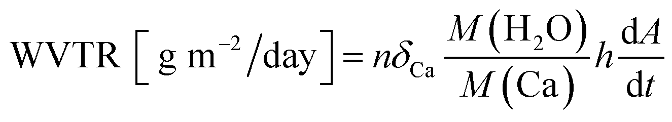 | (1) |
3. Results and discussion
A schematic illustration of the water-/oil-repellent multilayer TFE is provided in Fig. 1(a). The water-/oil-repellent multilayer TFE in this work is composed of two dyads of alternating iCVD deposited pV4D4, and a ALD deposited Al2O3 layer covered with the stacked hydrophobic polymer film. The deposition temperature of the iCVD and ALD processes was maintained at 38 °C and 90 °C to minimize any potential thermal damage to the organic electronic devices. An adjustment can also be made to the number of dyads of the TFE, but the dyad number was fixed to two in this work unless stated otherwise.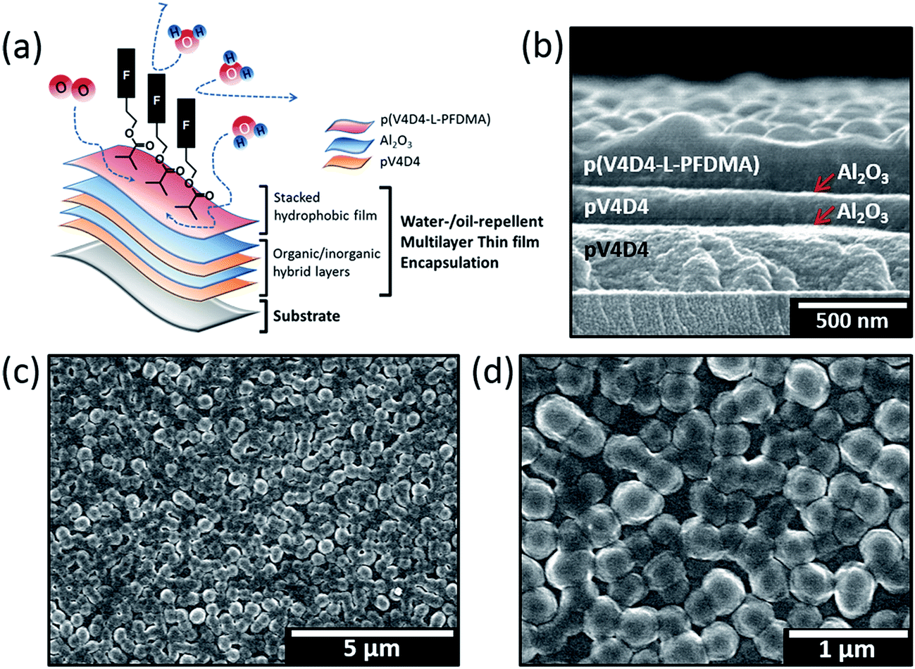 | ||
| Fig. 1 (a) A schematic diagram of the water-/oil-repellent multilayer TFE. A stacked hydrophobic polymer film consisting of pV4D4 (150 nm)/pPFDMA (350 nm) is deposited on the multilayer TFE composed of alternating organic (pV4D4)/inorganic (Al2O3) hybrid layers. (b) A cross-sectional SEM image of the water/oil-repellent multilayer TFE. Top-view SEM images of the water-/oil-repellent multilayer TFE with magnifications of (c) 10000× and (d) 30000×. | ||
In the stacked hydrophobic film, the top pPFDMA layer was covalently bound with the pV4D4 film underneath via vinyl groups,30 which substantially improved the mechanical and chemical stability of the hydrophobic layer. FTIR spectrum of the stacked hydrophobic film synthesized via the iCVD process contains both the peak of the cyclic siloxane ring of pV4D4 ranging from 1065 cm−1 to 1075 cm−1, and the sharp peak of CF2–CF3 functionality of pPFDMA at 1153 cm−1, indicating that the stack of pV4D4/pPFDMA was successfully formed without losing the characteristic functionality of each polymer film, as shown in Fig. S1.†
The cross-sectional SEM image clearly demonstrates that the stacked hydrophobic pV4D4 (150 nm)/pPFDMA (350 nm) layer was monolithically integrated onto the two-dyad pV4D4/Al2O3 multilayer TFE (Fig. 1(b)). The conformal integration of the hydrophobic layer is highly important to the long-term stability of the anti-contamination performance by preventing delamination from the multilayer TFE. A tape test and ultrasonication were applied to the hydrophobic film, and no delamination was observed, indicating the strong adhesion of the hydrophobic layer on the TFE.
The monolithic integration of the hydrophobic layer enabled the total thickness of the encapsulation layer to remain ultralow, just about 1.3 μm, which is extremely advantageous to retaining the high flexibility of the barrier film. The surface morphology of the hydrophobic pV4D4/pPFDMA layer (SEM images shown in Fig. 1(c) and (d)) was not simply flat, but was highly textured, with nano-ball-like structures with an average size of about 347 ± 42 nm evenly formed on the surface. The crystalline nature of the fluoroalkyl side chain of pPFDMA induced island growth during the iCVD process, resulting in this unique surface morphology, which was analogous to the previous observations reported for poly(1H,1H,2H,2H-perfluorodecyl acrylate) (pPFDA).35
The AFM image shown in Fig. S2(a)† indicates that the surface of the bare organic/inorganic TFE with an ALD Al2O3 top layer was flat, with a root-mean-square (RMS) surface roughness of 0.92 nm. The flat surface of the multilayer TFE is highly desirable to ensure the formation of conformal contact between the organic and inorganic layer.36 On the other hand, the surface of the stacked hydrophobic film integrated monolithically onto the multilayer TFE was highly bumpy, with a uniform spherical morphology, and AFM analysis indicates the RMS roughness had been greatly increased to 27.51 nm (Fig. S2(b)†), which is fully consistent with the SEM observation in Fig. 1(c) and (d).
The increase in surface roughness produced by the unique, nano-ball-like morphology of the hydrophobic layer led to an increase in the hydrophobicity of the surface-modified TFE, which is clearly illustrated in the water and hexadecane contact angle analysis shown in Fig. 2. While the hydrophilic bare glass substrate showed a low water contact angle (36.3 ± 2.1°), the deposition of two dyads of the organic/inorganic multilayer TFE increased the water contact angle to 90.7 ± 2.3°, and a further increase in the water contact angle to 121.9 ± 4.9° was observed following application of the stacked hydrophobic film on the multilayer TFE. Hexadecane (γ = 27.7 mN m−1) is an organic liquid widely used to assess the degree of oleophobicity.37 The bare glass and the multilayer TFE-coated glass were highly oleophilic and completely wet with hexadecane. The application of the stacked hydrophobic film on the multilayer TFE significantly improved the oleophobic performance of the barrier, as the hexadecane contact angle was changed to 75.3 ± 4.7°. Such hydrophobic and oleophobic behavior can be ascribed to the low surface energy of the outermost pPFDMA film coupled with its bumpy surface nanostructure.
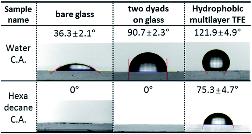 | ||
| Fig. 2 Water and hexadecane contact angles on bare glass (left), on two dyads of the organic/inorganic multilayer TFE (middle), and on the water-/oil-repellent multilayer TFE (right). | ||
This simple process of fabricating superior hydrophobic surfaces with unique nano-structures without any pre- or post-treatment is highly desirable for incorporating excellent water-/oil-repellency on the encapsulation layer.29
To investigate the anti-contamination properties of the hydrophobic surface to oil contaminants,7 several types of oil species were dropped on flat and tilted surfaces of pristine TFE, and hydrophobic TFE deposited on Ca film (Fig. 3). Fig. 3(a) presents dyed PDMS oil, olive oil, mineral oil and hexadecane droplets on two dyads of the organic/inorganic multilayer TFE-coated glass. The pristine TFE substrate was highly wettable with oil and left on oil stain on the surface. However, the oil contact angle became higher on hydrophobic TFE (Fig. 3(b)). On a 45°-tilted hydrophobic surface, which is specified in many standard weathering test methods (i.e. International Standardization Organization 1514:2004(E)),15 the oil droplets immediately slid down and no oil stain remained on the surface, as shown in Fig. 3(c).
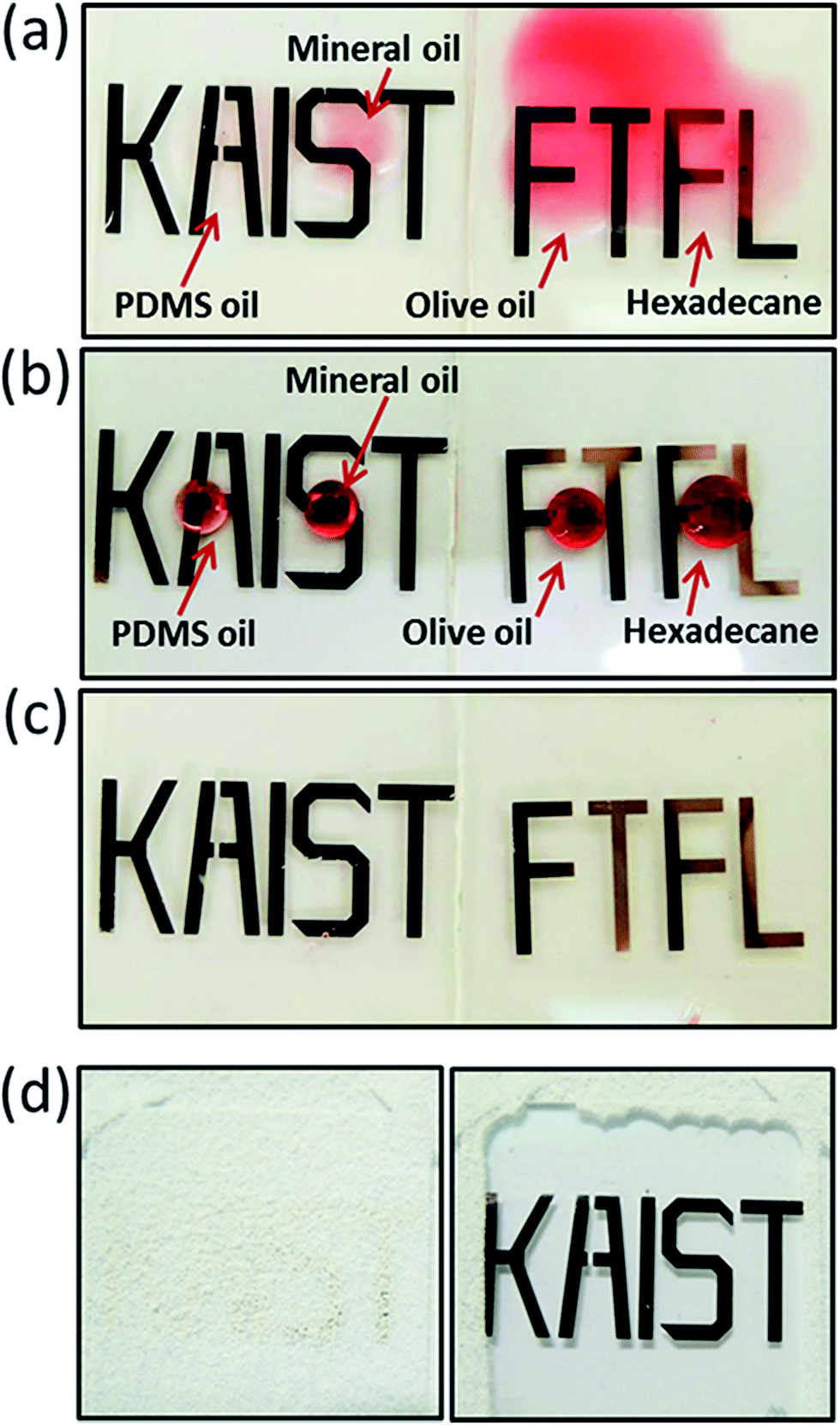 | ||
| Fig. 3 Oil stain test using PDMS oil, mineral oil, olive oil and hexadecane droplets (from left to right) (a) on two dyads of the organic/inorganic multilayer TFE, and (b) on the water-/oil-repellent multilayer TFE. (c) Tilting the water-/oil-repellent multilayer TFE substrate at 45° completely removes all oil droplets. ‘KAIST’ and ‘FTFL’ shown in the figures are Ca film deposited on the glass substrates before applying the organic/inorganic multilayer TFE. (d) Self-cleaning performance test on the water-/oil-repellent multilayer TFE tilted at 45°. Before (left) and after (right) rinsing the SiO2 powders with water droplets. | ||
The results of the oil stain tests clearly demonstrate that reductions in light absorption due to surface contamination of OPV devices can be minimized by application of the water-/oil-repellent multilayer TFE onto the OPV module. The water-/oil-repellent multilayer TFE ensures the long term cleanliness of the OPV module surface.
The self-cleaning effect of the water-/oil-repellent multilayer TFE was also investigated, as shown in Fig. 3(d). Silica powders with the sizes higher than 230 mesh were evenly distributed on the surface of the water-/oil-repellent multilayer TFE (left images in Fig. 3(d)), and rinsed with water droplets (right images of Fig. 3(d)). As expected, at the tilting angle of 45°, the distributed silica particles were completely removed with only few water droplets left on the surface of the hydrophobic multilayer TFE.
In contrast, without the water-/oil-repellent multilayer TFE, water droplets did not roll off, and thus, the particles remained on the substrate, as demonstrated in Fig. S3 and Movie S1.† These observations clearly illustrate that the hydrophobic surface modification can substantially improve self-cleaning performance, which is another critical factor affecting the light absorption into the OPV module. Note that no Ca oxidation was observed on the substrates sealed with both pristine TFE and hydrophobic multilayer TFE during the whole process of checking the anti-contamination performance, as can be seen in Fig. 3. This suggests that the water-/oil-repellent multilayer TFE totally retains its barrier property. The barrier performance was basically provided by the multilayer TFE, with the enhanced water-/oil-repellency and self-cleaning performance added by the monolithically integrated hydrophobic surface layers.
For OPV application, the refractive index of each layer comprising the multilayer barrier film should be close to each other in order to minimize the Fresnel reflection loss of light through the encapsulation layers.38 Fig. 4(a) summarizes the refractive indices of 30 nm-thick ALD Al2O3 film, 150 nm-thick iCVD pV4D4, and 350 nm-thick pPFDMA film deposited via iCVD process in the spectral range of 380 nm to 800 nm, as measured by ellipsometry. The average refractive index values of Al2O3, pV4D4 and pPFDMA were 1.54, 1.48 and 1.35, respectively. The refractive indices between Al2O3, and pV4D4 were close enough to avoid destructive interference. Also, with the addition of the pPFDMA film on top of the pV4D4 film, a stepwise increase in the refractive indices from air to pV4D4 film was formed. Thus, the high transparency of the barrier film was ensured, which is an essential feature to minimize light reflectance in the OPV.
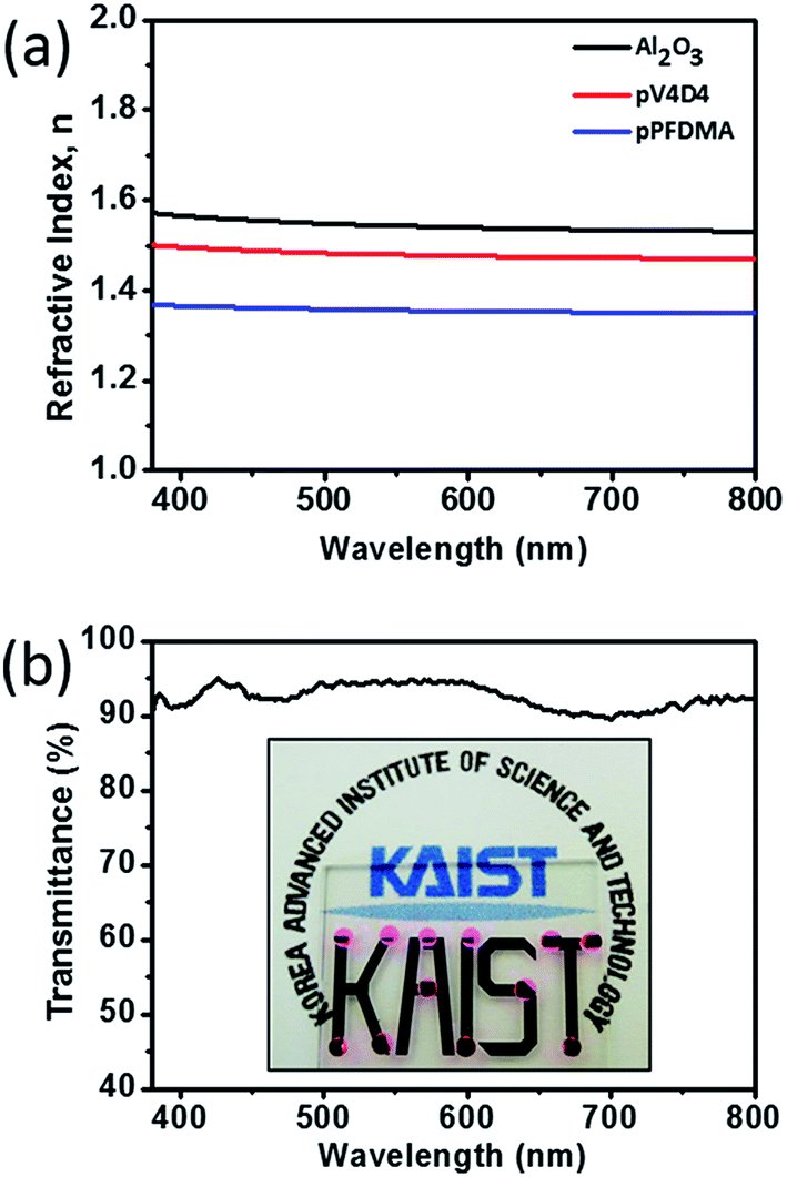 | ||
| Fig. 4 (a) Refractive indices of Al2O3, pV4D4, and pPFDMA. (b) Transmittance value of the water-/oil-repellent multilayer TFE on glass. Inset image in (b) is a digital camera image of a glass coated with the water-/oil-repellent multilayer TFE. The black ‘KAIST’ logo is Ca film deposited beneath the TFE, and the pink droplets are water dispersed on the TFE. It can be observed that the TFE has high transparency, hydrophobicity, and barrier properties. | ||
Fig. 4(b) shows the transmittance spectrum of the hydrophobic multilayer TFE on glass in the wavelength range of 380 nm to 800 nm. The measured average transmittance was about 92.5% with a minimum transmittance of 89.6% at 700 nm, including the glass substrate, indicating that the water-/oil-repellent multilayer TFE is highly transparent, as shown in the inset of Fig. 4(b).
In order to measure the water vapor and oxygen barrier performance of the water-/oil-repellent multilayer TFE, a Ca test was carried out, according to the method proposed by Bertrand et al.39 Fig. 5(a) shows the result of the WVTR measurement. The WVTR values for the water-/oil-repellent multilayer TFE were measured under accelerated condition at 38 °C with 90% RH. In the case of the water-/oil-repellent multilayer TFE, the stacked hydrophobic film of pV4D4 (150 nm)/pPFDMA (350 nm) was deposited on the two dyads of the organic/inorganic multilayer TFE, as shown in Fig. 1(b). The obtained WVTR value was compared with control multilayer TFEs having (case 1) two dyads of the organic/inorganic multilayer TFE without any additional layer, and (case 2) two dyads of the organic/inorganic multilayer TFE with additional pV4D4 film (500 nm) on the surface. The measured WVTR value of (case 1), the two dyads of the organic/inorganic multilayer TFE without any additional layer was 6.2 ± 3.8 × 10⁻³ g m−2 d−1. The WVTR value was decreased to 4.7 ± 0.5 × 10⁻³ g m−2 d−1 for (case 2), with the additional 500 nm-thick pV4D4 film on two dyads TFE.
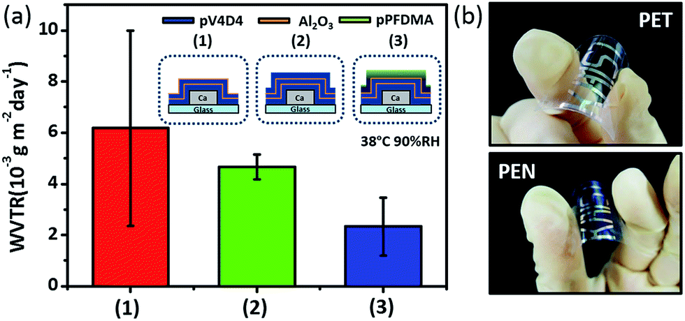 | ||
| Fig. 5 (a) The WVTR values of (case 1) two dyads of the organic/inorganic multilayer TFE without any additional surface layer, (case 2) two dyads of the organic/inorganic multilayer TFE with additional pV4D4 film (500 nm) on the surface, and (case 3) the water-/oil-repellent multilayer TFE (the two dyads TFE coated with pV4D4 (150 nm)/pPFDMA (350 nm)). (b) Images showing flexing of the water-/oil-repellent multilayer TFE on PET (top) and PEN (bottom) substrates. | ||
Furthermore, with the stacked hydrophobic film of pV4D4 (150 nm)/pPFDMA (350 nm) deposited on the two dyads TFE, the WVTR value was further decreased to 2.3 ± 1.1 × 10⁻³ g m−2 d−1 (case 3), which corresponds to 1.1 × 10⁻⁴ g m−2 d−1 at ambient condition (25 °C with 50% RH) considering the acceleration factors.14 The slight decrease in the WVTR is most likely due to the increased hydrophobicity provided by the iCVD coating.
The Ca test results clearly indicate that the additional application of the stacked hydrophobic layer onto the multilayer TFE did not degrade the barrier performance of the multilayer TFE, which is fully consistent with the results in Fig. 3 and 4. This lack of apparent degradation of the barrier performance of the underlying TFE after the monolithic incorporation of the hydrophobic layer is one of the highly advantageous characteristics of the iCVD process. The process requires relatively gentle deposition condition, and is completely solvent-free. This observation strongly infers that the barrier performance and other properties of the TFE can be optimized independently without considering the degradation of barrier properties by adding the hydrophobic layer. Therefore, further optimization of the underlying organic/inorganic multilayer can enhance the barrier property as well as flexibility of the TFE. For example, the inorganic layer can be substituted with Al2O3 nano-laminated with ZrO2 to improve the barrier property.11 Also, the TFE structure of the layers can be changed in order to further optimize both the barrier property and flexibility.14
For future application on to flexible electronics, the barrier film needs to be highly flexible. The ultrathin, 1.3 μm-thick hydrophobic multilayer TFE developed in this work was is applicable to flexible substrates as well. To demonstrate this, the hydrophobic multilayer TFE was deposited to encapsulate a Ca film on PET and PEN substrates, which are commonly used as substrates for flexible electronic devices, encapsulating Ca film, as shown in Fig. 5(b) and Movie S2.† The barrier performance and the hydrophobic property of the TFE film were preserved even on the bendable PET and PEN films. As shown in Fig. S4,† three dyads of pV4D4/Al2O3 multilayer was deposited onto both glass and 25 μm-thick PEN substrates. Unlike glass substrates, PEN substrates are highly leaky to water vapor, and the PEN substrate was pre-deposited with three dyads of a pV4D4/Al2O3 layer to prevent the leakage of water vapor and/or oxygen through the PEN side. An additional pV4D4 layer was deposited to smoothen the top-most Al2O3 layer before Ca deposition. A Ca test was performed on both substrates as described in the manuscript and the measured WVTR of the TFE's on glass and PEN substrates were 2.3 × 10⁻⁴ and 4.0 × 10⁻⁴ g m−2 d−1, respectively, under accelerated condition of 38 °C, 90% RH. Note that in our TFE configuration, the iCVD polymer layer, pV4D4, is always deposited first on the substrate before the ALD process. Therefore, the Al2O3 layer, the main component determining the barrier property of the multilayer, is always grown on the same pV4D4 surface, regardless of the substrate materials. Thus, the quality of the inorganic layer should also be constant even if the substrate material is changed. From this result, we can conclude that the effect of substrate material on the barrier performance of the multilayers is not significant.
The multilayer was flexed 1000 times with a bending radius of 10 mm. Even after the repeated flexing, the WVTR change was within error range, suggesting that the barrier properties were not affected. The result is shown in Fig. S4(c).† Following further investigation considering flexibility, this hydrophobic multilayer encapsulation can be applied to flexible electronics.
4. Conclusion
To summarize, a water-/oil-repellent multilayer TFE with both excellent anti-contamination and barrier properties was successfully achieved by the monolithic integration of a robust hydrophobic surface layer onto a multilayer TFE, without damaging the underlying substrates. The monolithic fabrication method adopted in this work utilized alternating depositions with iCVD and ALD processes under mild process conditions, to minimize the potential damage to the organic electronic devices. The surface of the TFE layer was highly water-/oil-repellent due to the deposition of the stacked hydrophobic film. The water-/oil-repellent multilayer TFE exhibited high transparency, with a transmittance of 92.5%. It was effectively self-cleaning against dust and oil contaminants, and exhibited excellent barrier properties, with a WVTR as low as 2.3 ± 1.1 × 10⁻³ g m−2 d−1 at 38 °C with 90% RH, which is equivalent to 1.1 × 10⁻⁴ g m−2 d−1 at ambient condition. The encapsulation performance was not deteriorated by the addition of the stacked hydrophobic layer.Further research can optimize and enhance the barrier and mechanical properties of the underlying organic/inorganic multilayer for the novel TFE to be applied onto the OPVs. In addition, the applicability on flexible substrate was also demonstrated. Advancement in the mechanical properties of the underlying organic/inorganic layer can provide a new insight for the development of encapsulation systems for highly flexible organic electronic devices for outdoor usage.
Acknowledgements
This work was partly supported by Institute for Information & communications Technology Promotion (IITP) grant funded by the Korea government (MSIP) (B0101-15-0133, The core technology development of light and space adaptable energy-saving I/O platform for future advertising service), and Graphene Materials and Components Development Program of MOTIE/KEIT (10044412, Development of basic and applied technologies for OLEDs with graphene).References
- M. Berggren, D. Nilsson and N. D. Robinson, Nat. Mater., 2007, 6(1), 3 CrossRef CAS PubMed
.
- T. W. Kelley, P. F. Baude, C. Gerlach, D. E. Ender, D. Muyres, M. A. Haase, D. E. Vogel and S. D. Theiss, Chem. Mater., 2004, 16, 4413 CrossRef CAS
- M. C. Scharber and N. S. Sariciftci, Prog. Polym. Sci., 2013, 38(12), 1929 CrossRef CAS PubMed
- F. Deschler, D. Riedel, B. Ecker, E. von Hauff, E. Da Como and R. C. I. MacKenzie, Phys. Chem. Chem. Phys., 2013, 15(3), 764 RSC
- M. Jorgensen, K. Norrman and F. C. Krebs, Sol. Energy Mater. Sol. Cells, 2008, 92(7), 686 CrossRef PubMed
- M. S. El-Shobokshy and F. M. Hussein, Renewable Energy, 1993, 3, 585 CrossRef CAS
- K. Fukada, S. Nishizawa and S. Shiratori, J. Appl. Phys., 2014, 115(10), 103516 CrossRef PubMed
- P. E. Burrows, V. Bulovic, S. R. Forrest, L. S. Sapochak, D. M. Mccarty and M. E. Thompson, Appl. Phys. Lett., 1994, 65(23), 2922 CrossRef CAS PubMed
- S. W. Seo, E. Jung, S. J. Seo, H. Chae, H. K. Chung and S. M. Cho, J. Appl. Phys., 2013, 114(14), 143505 CrossRef PubMed
- D. S. Han, D. K. Choi and J. W. Park, Thin Solid Films, 2014, 552, 155 CrossRef CAS PubMed
- S. W. Seo, E. Jung, H. Chae and S. M. Cho, Org. Electron., 2012, 13, 2436 CrossRef CAS PubMed
- Y. C. Han, E. Kim, W. Kim, H. G. Im and B. S. Bae, Org. Electron., 2013, 14, 1435 CrossRef CAS PubMed
- H. Zhang, H. Ding, M. Wei, C. Li, B. Wei and J. Zhang, Nanoscale Res. Lett., 2015, 10, 169 CrossRef PubMed
- S. W. Seo, H. Chae, S. J. Seo, H. K. Chung and S. M. Cho, Appl. Phys. Lett., 2013, 102, 161908 CrossRef PubMed
- Y. B. Park, H. Im, M. Im and Y. K. Choi, J. Mater. Chem., 2011, 21(3), 633 RSC
- E. J. Park, J. K. Sim, M. G. Jeong, H. O. Seo and Y. D. Kim, RSC Adv., 2013, 3(31), 12571 RSC
- J. H. Choi, Y. M. Kim, Y. W. Park, T. H. Park, K. Y. Dong and B. K. Ju, Langmuir, 2009, 25(12), 7156 CrossRef CAS PubMed
- J. H. Choi, Y. M. Kim, Y. W. Park, T. H. Park, K. Y. Dong and B. K. Ju, Nanotechnology, 2009, 20(13), 135303 CrossRef PubMed
- S. H. K. Park, J. Oh, C. S. Hwang, J. I. Lee, Y. S. Yang and H. Y. Chu, Electrochem. Solid-State Lett., 2005, 8(2), H21 CrossRef CAS PubMed
- J. Granstrom, J. S. Swensen, J. S. Moon, G. Rowell, J. Yuen and A. J. Heeger, Appl. Phys. Lett., 2008, 93(19), 193304 CrossRef PubMed
- S. H. Kim, W. M. Yoon, M. Jang, H. Yang, J. J. Park and C. E. Park, J. Mater. Chem., 2012, 22(16), 7731 RSC
- Y. J. Liao, F. F. Yu, L. Long, B. Wei, L. Lu and J. H. Zhang, Thin Solid Films, 2011, 519(7), 2344 CrossRef CAS PubMed
- R. L. Puurunen, J. Appl. Phys., 2005, 97(12), 121301 CrossRef PubMed
- W. E. Tenhaeff and K. K. Gleason, Adv. Funct. Mater., 2008, 18(7), 979 CrossRef CAS PubMed
- D. A. Spee, M. R. Schipper, C. H. M. van der Werf, J. K. Rath and R. E. I. Schropp, Thin Solid Films, 2013, 532, 84 CrossRef CAS PubMed
- A. M. Coclite, G. Ozaydin-Ince, F. Palumbo, A. Milella and K. K. Gleason, Plasma Processes Polym., 2010, 7(7), 561 CrossRef CAS PubMed
- M. C. Barr, J. A. Rowehl, R. R. Lunt, J. J. Xu, A. N. Wang, C. M. Boyce, S. G. Im, V. Bulovic and K. K. Gleason, Adv. Mater., 2011, 23(31), 3500 CrossRef CAS PubMed
- B. J. Kim, D. H. Kim, S. Y. Kang, S. D. Ahn and S. G. Im, J. Appl. Polym. Sci., 2014, 131(24), 40974 Search PubMed
- Y. Yoo, J. B. You, W. Choi and S. G. Im, Polym. Chem., 2013, 4(5), 1664 RSC
- J. S. Lewis and M. S. Weaver, IEEE J. Sel. Top. Quantum Electron., 2004, 10(1), 45 CrossRef CAS
- S. H. Baxamusa, S. G. Im and K. K. Gleason, Phys. Chem. Chem. Phys., 2009, 11(26), 5227 RSC
- T. Hirvikorpi, R. Laine, M. Vaha-Nissi, V. Kilpi, E. Salo, W. M. Li, S. Lindfors, J. Vartiainen, E. Kentta, J. Nikkola, A. Harlin and J. Kostamo, Thin Solid Films, 2014, 550, 164 CrossRef CAS PubMed
- C. A. Wilson, R. K. Grubbs and S. M. George, Chem. Mater., 2005, 17, 5625 CrossRef CAS
- N. P. Kobayashi, C. L. Donley, S. Y. Wang and R. S. Williams, J. Cryst. Growth, 2007, 299, 218 CrossRef CAS PubMed
- A. M. Coclite, Y. J. Shi and K. K. Gleason, Adv. Mater., 2012, 24(33), 4534 CrossRef CAS PubMed
- J. Lewis, Mater. Today, 2006, 9(4), 38 CrossRef CAS
- J. P. Zhang and S. Seeger, Angew. Chem., Int. Ed., 2011, 50(29), 6652 CrossRef CAS PubMed
- X. Yan, F. W. Mont, D. J. Poxson, M. F. Schubert, J. K. Kim, J. Cho and E. F. Schubert, Jpn. J. Appl. Phys., 2009, 48(12), 120203 CrossRef
- J. A. Bertrand and S. M. George, J. Vac. Sci. Technol., A, 2013, 31(1), 01A122 Search PubMed
Footnotes |
| † Electronic supplementary information (ESI) available. See DOI: 10.1039/c5ra10425d |
| ‡ These authors contributed equally to this work. |
| This journal is © The Royal Society of Chemistry 2015 |