DOI:
10.1039/C5RA10351G
(Paper)
RSC Adv., 2015,
5, 65005-65009
Controllable electrophoresis deposition of TiO2 mesoporous spheres onto Ti threads as photoanodes for fiber-shaped dye-sensitized solar cells
Received
1st June 2015
, Accepted 24th July 2015
First published on 24th July 2015
Abstract
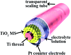
Complex TiO2 mesoporous spheres (MSs) were deposited on a Ti thread using an electrophoresis deposition (EPD) technique as working electrodes of the fiber-shaped dye-sensitized solar cell (FDSSC). The thickness of the TiO2 MS film can be controlled by altering EPD time in a constant voltage. Electrochemical impedance spectroscopic measurement demonstrates the film thickness-dependent photovoltage performance of the FDSSC. The total conversion efficiency of the FDSSC achieves 3.8% through optimizing the thickness of the film.
Introduction
Dye-sensitized solar cells (DSSCs) have received considerable interest due to their flexibility, low cost to produce, high conversion efficiency.1 However, their flat-shape limits their application in many fields. Compared with flat DSSC's counterpart, the fiber-shaped DSSC (FDSSC) has many advantages, such as being ITO free, lightweight, flexible, and integrable into textiles.2,3 FDSSCs can be generally fabricated by twisting two fiber-like electrodes together, in which one wire coated by active layers (e.g. TiO2) serves as a working electrode and the other (e.g. Pt) as a counter electrode.4 Currently, two approaches are available to fabricate the photoanode of the FDSSC. Dip-coating method is an easy and fast way by immersing a fiber into prepared TiO2 colloids.5 However it can not control the thickness and uniformity of the film accurately. The other is anodic or chemical ways to grow nanostructured semiconductors directly on a fiber.6–8 Nevertheless, these methods are limited by only generating nanotubes and nanowires.
Electrophoresis deposition (EPD) is a traditional ceramic technique and is gaining increasing interest both in academia and in the industrial sector as a technique to produce advanced materials.9 EPD is essentially a two-step process; in the first step, charged particles dispersed in a solvent are forced to move toward an electrode by applying an electric field to the suspension; in the second step, the particles accumulate at one of the electrode and form a coherent deposition.10 The advantage of the EPD technique lies in complexly shaped objects can be coated using EPD, so to can it be used for shaping objects.11 EPD also offers additional merit of requiring simple equipment, low cost, higher speed, process simplicity, deposit thickness controllable. The EPD approach has been employed to fabricate various photoelectrodes of flat-shape DSSC, such as depositing diverse TiO2 nanostructures e.g. “sea urchin”-like architecture,12 nanorod,13 nanoparticle14 as photoanodes, and Pt nanoparticles,15 carbon nanotubes,16 and graphene17 as counter electrodes on both plate and flexible conductive substrates.
The TiO2 mesoporous spheres (MSs) are composed of anatase TiO2 nanocrystals together to form larger secondary particles. Advantageously to traditional nanoparticles, the use of submicrometer-sized TiO2 beads with abundant mesopores promote light scattering in DSSCs and the accessible surface for dye loading insure the photon-to-current conversion efficiency.18,19 In this paper, we for the first time successfully apply the EPD technique to fabricate FDSSC by depositing TiO2 MS onto a Ti wire as a photoanode. The total conversion efficiency of the FDSSC achieves 3.8% through optimizing the thickness of the TiO2 MS film by changing EPD time. Our work proves the EPD feasibility of coating complex nanostructures on highly curved fiber substrates to promote the conversion efficiency of the FDSSC.
Experiment
Preparation of TiO2 MSs
Typically, the TiO2 MS was prepared according to the literature methods.19 Firstly, 2.14 g of titanium(IV)tetraethoxide and 0.83 g of hexadecylamine were dissolved in 62.5 mL ethanol, and 0.788 mL of 0.1 M NaCl aqueous solution in a separate 62.5 mL ethanol. Mixing two ethanol solutions at room temperature and the TiO2 particles was collected by repeating centrifugation (12
000 rpm) and washed with ethanol several times. Then TiO2 particles were dispersed in a mixture of 48 mL ethanol and 24 mL water. The mixtures were sealed within a Teflon-lined autoclave heated at 160 °C for 16 h. The solid products were collected by centrifugation and washed with ethanol then sintered at 500 °C for 30 min.
Preparation of photoanode
Ti wires (diameter: 250 μm) was subjected to supersonic treatment in acetone for 10 min, then washed by ethanol and deionized water. 0.01 M titanium isopropoxide ethanol solution and 0.02 M acetylacetone ethanol solution was prepared as the dense TiO2 layer (DTL) solution. Then the Ti wire was dipped in the solution for 30 s then taken out and sintered at 500 °C for 15 min. The photoanodes were fabricated using EPD method. The powder suspension for EPD was prepared by dispersing iodine (10 mg) and TiO2 powder (40 mg) in acetone (50 mL) with the assistance of supersonic treatment. EPD process was conducted between two parallel Ti wires with the length of ∼5 cm under 40 V of bias for few minutes, in which the Ti wire treated with DTL was used as the cathode and pure Ti wire as the anode. The EPD-treated electrode was dried in air, and sintered at 500 °C for 30 min with a heating rate of 5 °C min−1. At last the electrode was immersed in a 0.2 M TiCl4 solution bath at 70 °C for 30 min, taken out and then sintered at 450 °C for 30 min with a heating rate of 5 °C min−1 to improve the connection among TiO2 MSs. The Ti wire was then placed into the 0.5 mM N719 dye solution (solvent mixture of acetonitrile and tert-butyl alcohol in volume ratio of 1
:
1) for 24 h at room temperature. Lastly, it was taken out and rinsed with absolute ethanol to obtain the dye-sensitized photoanode.
Preparation of FDSSC
The photoanode and platinum wire (diameter: 100 μm) were twisted together and then inserted into a transparent capillary filled with electrolyte. The two ends of the capillary were sealed with wax to prevent evaporation of the electrolyte. The electrolyte used in the experiment was made up of 1.0 M 1-butyl-3-methylimidazolium iodide (BMIMI), 50 mM LiI, 30 mM I2 and 0.5 M tert-butylpyridine in a mixed solvent of acetonitrile and valeronitrile (v/v, 85
:
15).
Characteristics of cell performance
I–V (current–voltage curves) data are acquired with the length FDSSC of 3 cm, on a Keithley 236 source measurement unit under AM 1.5 illumination cast by an Oriel 92251A-1000 sunlight simulator calibrated by the standard reference of a Newport 91150 silicon solar cell. Electrochemical impedance spectroscopic (EIS) curves of the FDSSCs were also observed with PAR2273 workstation (Princeton Applied Research, USA). The frequency range is set from 50 mHz to 100 kHz. In the dye adsorption test, 0.1 M NaOH was used to remove the dye on the photoanode, ultraviolet visible spectroscopy (UV-vis spectroscopy) was utilized to examine the content of the dye.
Results and discussion
The XRD pattern demonstrates that the MS TiO2 acquired is in anatase crystal form (Fig. 1). Anatase phase is of higher conduction-band edge energy than rutile phase and thus electron transport is faster in the anatase phase, which causes anatase to become the preferred phase for DSSCs.20 The field-emission scanning electron microscopy (FE-SEM) images show that the as-synthesized TiO2 MS exhibits a well-defined spherical morphology with size typically ranging from 600 to 800 nm (Fig. 2a and b), comparative to optical wavelength to promote light scattering. The TiO2 MS displays rough surfaces and consists of many tiny nanocrystals. The considerable mesopores makes the TiO2 MS possess high surface area, which ensures the dye absorption of the film. The TEM image further demonstrates that the TiO2 MS is built of small particles with the size of 10–20 nm (Fig. 2b′). The high-resolution TEM image of the nanocrystals clearly shows a lattice fringe of ∼0.35 nm, corresponding to the (101) lattice plane of anatase TiO2 (inset of Fig. 2b′).
 |
| Fig. 1 XRD pattern of the TiO2 MS. | |
 |
| Fig. 2 (a and b) SEM images of the prepared MS TiO2 at different magnification. (a′ and b′) TEM and HRTEM images of the TiO2 MS at different magnification. (c) The top view of Ti wire. (d and e) The top view of Ti wire after EPD of 150 s at different magnification. (f) Cross-section view of Ti wire after EPD of 150 s. | |
For the EPD process, a Ti thread with smooth surface and diameter of 250 μm was used as a deposition substrate (Fig. 2c). After the EPD process under a bias of 40 V for 150 second deposition, the Ti wire became obviously rough and was entirely surrounded with the target materials (Fig. 2d). The FE-SEM images of the top and cross section of the treated Ti wire reveal that numerous TiO2 MS were densely covered on the whole Ti wire (Fig. 2d–f). The thickness of the film was estimated about ∼5 μm. The film thickness can be controlled by altering EPD deposition time in a constant voltage EPD. The ∼3 μm and ∼6 μm thickness of the TiO2 MS film can be obtained with the EPD time of 120 second and 180 second, respectively.
The TiO2 MS-coated Ti thread as a photoanode twisted with a Pt wire as counter electrode was inserted into a transparent capillary filled with electrolyte to be assembled into a FDSSCs (Fig. 3a), as schematically illustrated in Fig. 3b. Fig. 4 shows the J–V curves of FDSSCs with different photoanodes and the corresponding photovoltaic data was listed in Table 1. S120, S150, and S180 were referred to the cells with the different photoanodes fabricated with the EPD times of 120 s, 150 s, and 180 s respectively, followed by treatment with TiCl4, which allows to improve connection among the TiO2 MS. S150-no TiCl4 was delegated to the EPD time of 150 s without TiCl4 treatment. It is clear that the TiCl4 treatment obviously influences the performance of the cell by improving the short circuit density from 4.16 mA cm−2 of S150-no TiCl4 to 7.12 mA cm−2 of S150. Improved connections among the TiO2 MS allows the electrons to transport from one bead to another more facility, thus lowering the recombination of electrons and holes.20 While S120, S150, and S180 are of comparable values of Voc and FF, S150 achieves the highest Jsc compared with S120 and S180. Therefore, high Jsc ensures a better photovoltaic performance of S150. In comparison of S150 with S120, the increased thickness of the film enables S150 to absorb more dye (Table 2), leading to more number of electron injection from the dye to TiO2, thus resulting in a higher Jsc. However, although S180 is of thicker film than S150, the former inconsequentially displays a relatively lower Jsc, causing the cell efficiency decreased. We believe that the unexpectedly photovoltage performance between S150 and S180 cells originates their different MS packing behaviour in the film. For S180, at initial deposition time, higher current density and applied potential exerts more pressure on particle flux and movement, producing tightly and densely packed TiO2 MS films from a dispersion of the MS. However, with the time longer and the film thicker, the current density and applied voltage drops across the film, which leads the electrostatic attraction toward the MS to becoming weak. It makes poor interconnection among MSs in the subsequent outer layer of S180, which result in increased resistance to electron transport, negatively affecting the cell performance. For comparison, commercial P25 TiO2 powder-based FDSSC was also fabricated with the same EPD process of S150. The photoelectrical measurement demonstrates that S150 displays both higher Voc and Jsc than P25, due to special mesoporous sphere structure with the ability of intense light scattering and large surface area, as shown in Fig. 4 and Table 1.
 |
| Fig. 3 (a) Photograph of the FDSSC and (b) the corresponding schematic setup. | |
 |
| Fig. 4 J–V curves of FDSSCs of photoanode with different EPD times of 120 s, 150 s, 180 s, and P25 following with TiCl4 treatment, and EPD times of 150 s without TiCl4 treatment. The counter electrode is a platinum wire. | |
Table 1 I–V characteristics of FDSSCs
FDSSC |
Voc (V) |
Isc (mA cm−2) |
FF |
η (%) |
S120 |
0.736 |
6.36 |
0.714 |
3.34 |
S150 |
0.760 |
7.12 |
0.702 |
3.80 |
S180 |
0.746 |
6.73 |
0.716 |
3.60 |
S150-no TiCl4 |
0.761 |
4.16 |
0.689 |
2.18 |
P25 |
0.698 |
3.36 |
0.721 |
1.69 |
Table 2 Electrochemical impedance spectroscopic parameters
FDSSC |
Rct (Ω) |
Rt (Ω) |
Dye absorption (mol cm−2) |
S120 |
180.2 |
9.6 |
4.18 × 10⁻⁸ |
S150 |
129.8 |
10.0 |
4.70 × 10⁻⁸ |
S180 |
106.8 |
11.8 |
5.29 × 10⁻⁸ |
To explore the deposition time-dependent photovoltage performance, S120, S150, and S180 were studied with EIS measurement, a powerful technique to identify and study the transport and recombination in the FDSSCs. Fig. 5 is Nyquist plots of different FDSSCs and the corresponding EIS data was listed in Table 2. The inset is the corresponding equivalent circuit. Rt is the electron transport resistance, which implies difficulty of electron transport in the film. Rct is a charge transfer resistance related to recombination of electrons in the TiO2 MSs and I3− in the electrolyte at the TiO2/electrolyte interface.21 The EIS data shows that S120 and S150 possess a similar Rt (∼4% deviation). In contrast, S180 has a higher Rt than S150 (∼18% deviation), which indicates a transport barrier in the TiO2 film of S180. Higher resistance in the TiO2 film causes the decrease in Jsc. In addition, S180 is of a lower Rct, implying that electron is easier to recombination with the I3− of the electrolyte rather than preferably transporting across the film.
 |
| Fig. 5 Nyquist plots of FDSSCs with different EPD times of 120 s, 150 s and 180 s. Inset: equivalent circuit for a solar cell. Rs is series resistance of the cell. RTT, CTT: contact resistance and capacitance at Ti/TiO2 interface. RTE, CTE: charge transfer resistance and double layer capacitance at the Ti/electrolyte interface. Rt is the charge transport resistance in TiO2 film. Rct is the charge transfer resistance at the TiO2/electrolyte interface. Cμ is the chemical capacitance of the MS TiO2. Rt = rtL, Rct = rct/L, Cμ = cμL, L is TiO2 film thickness. Zw: diffusion impedance in the electrolyte. RPt, CPt: charge transfer resistance and double layer capacitance at the Pt counter electrode/electrolyte interface. | |
Conclusion
The FDSSC based on the TiO2 MSs on Ti wires as photoanode by EPD method was fabricated with optimized conversion efficiency of 3.8%. The photovoltage performance is closely related with the film thickness. The result proves that use of the EPD to coat submicrometer-sized spheres on metal wire is a feasible method to fabricate the working electrode on the fiber substrate and may establish an industrial procedure to reproducibly produce FDSSCs.
Acknowledgements
This work was supported by 973 Programs (No. 2011CB933303, 2014CB239302, 2013CB632404), NSFC (No. 21301101 and 11174129), Natural Science Foundation of Jiangsu Province (No. BK2012015 and BK2011056), Jiangsu Technical support plan-industrial parts (BE2012089), Kunshan New industries multiplication plan science and technology special Fund (KX1202), The Natural Science Foundation of Henan Department of Education (14A150027), Natural Science Foundation of Nanyang Normal University (No. ZX2014040).
References
- A. Hagfeldt, G. Boschloo, L. C. Sun, L. Kloo and H. Pettersson, Chem. Rev., 2010, 110, 6595 CrossRef CAS PubMed.
- T. Chen, L. B. Qiu, Z. B. Yang and H. S. Peng, Chem. Soc. Rev., 2013, 42, 5031 RSC and the references therein.
- D. C. Zou, Z. B. Lv, X. Cai and S. C. Hou, Nano Energy, 2012, 1, 273 CrossRef CAS PubMed and the references therein.
- X. Fan, Z. Z. Chu, F. Z. Wang, C. Zhang, L. Chen, Y. W. Tang and D. C. Zou, Adv. Mater., 2008, 20, 592 CrossRef CAS PubMed.
- Y. P. Fu, Z. B. Lv, H. W. Wu, S. C. Hou, X. Cai, D. Wang and D. C. Zou, Sol. Energy Mater. Sol. Cells, 2012, 102, 212 CrossRef CAS PubMed.
- Z. B. Lv, J. F. Yu, H. W. Wu, J. Shang, D. Wang, S. C. Hou, Y. P. Fu, K. Wu and D. C. Zou, Nanoscale., 2012, 4, 1248 RSC.
- L. Chen, Y. Zhou, H. Dai, Z. D. Li, T. Yu, J. G. Liu and Z. G. Zou, J. Mater. Chem. A, 2013, 1, 11790 CAS.
- Y. H. Wang, Y. Liu, H. X. Yang, H. Wang, H. Shen, M. Li and J. Yan, Curr. Appl. Phys., 2010, 10, 119 CrossRef PubMed.
- A. R. Boccaccini and I. Zhitomirsky, Curr. Opin. Solid State Mater. Sci., 2002, 6, 251 CrossRef CAS.
- O. O. van der Biest and L. J. Vandeperre, Annu. Rev. Mater. Sci., 1999, 29, 327 CrossRef CAS.
- A. R. Boccaccini, J. A. Roether, B. J. C. Thomas, M. S. P. Shaffer, E. Chavez, E. Stoll and E. J. Minay, J. Ceram. Soc. Jpn., 2006, 114, 1 CrossRef CAS.
- N. P. Benehkohal and G. P. Demopoulos, ChemSusChem., 2014, 7, 813 CrossRef CAS PubMed.
- F. Shao, J. Sun, L. Gao, J. Chen and S. Yang, RSC Adv., 2014, 4, 7805 RSC.
- W. Tan, X. Yin, X. Zhou, J. Zhang, X. Xiao and Y. Lin, Electrochim. Acta, 2009, 54, 4467 CrossRef CAS PubMed.
- X. Yin, Z. Xue and B. Liu, J. Power Sources, 2011, 196, 2422 CrossRef CAS PubMed.
- G. Zhu, L. Pan, T. Lu, X. Liu, T. Lv, T. Xu and Z. Sun, Electrochim. Acta, 2011, 56, 10288 CrossRef CAS PubMed.
- H. Choi, H. Kim, S. Hwang, Y. Han and M. Jeon, J. Mater. Chem., 2011, 21, 7548 RSC.
- D. H. Chen, F. Z. Huang, Y. B. Cheng and R. A. Caruso, Adv. Mater., 2009, 21, 2206 CrossRef CAS PubMed.
- Y.-C. Park, Y.-J. Chang, B.-G. Kum, E.-H. Kong, J. Y. Son, Y. S. Kwon, T. Park and H. M. Jang, J. Mater. Chem., 2011, 21, 9582 RSC.
- N.-G. Park, G. Schlichthorl, J. van de Lagemaat, H. M. Cheong, A. Mascarenhas and A. J. Frank, J. Phys. Chem. B, 1999, 103, 3308 CrossRef CAS.
- F. Fabregat-Santiago, J. Bisquert, G. Garcia-Belmonte, G. Boschloo and A. Hagfeldt, Sol. Energy Mater. Sol. Cells, 2005, 87, 117 CrossRef CAS PubMed.
|
This journal is © The Royal Society of Chemistry 2015 |
Click here to see how this site uses Cookies. View our privacy policy here.